NMI BRK IRQ handling

0041 BRK AND NMI ENTRY POINTS TO TIM
0042 -------------------------------
0043 
0044     TIM IS NORMALLY ENTERED WHEN A 'BRK' INSTRUKTION IS
0045         ENCOUNTERED DURING PROGRAM EXECUTION.  AT THAT
0046         TIME CPU REGISTERS ARE OUTPUT:    PC F A X Y SP
0047         AND CONTROL IS GIVEN TO THE KEYBOARD.
0048     USER MAY ENTER TIM BY PROGRAMMED BRK OR INDUCED NMI.  NMI
0049         ENTRIES CAUSE A '#' TO PRECEDE THE '.' IN THE CPU REGISTER
0050         PRINTOUT FORMAT
0051 
0052 NON-BRK INTRO (EXTERNAL DEVICE) INTERRUPT HANDLING
0053 --------------------------------------------------
0054 
0055     A NON-BRK INTRO INTERRUPT CAUSES AN INDIRECT JUMP TO THE ADDRESS
0056         LOCATED AT 'UINT' (HEX FFF8).  THIS LOCATION CAN BE SET
0057         USING THE ALTER CMD, OR LOADED AUTOMATICALLY IN PAPER TAPE
0058         FROM WITH THE LH CMD IF THE USER ASSIGNS HIS INTRO INTERRUPT
0059         VECTOR TO $FFF8 IN THE SOURCE ASSEMBLY PROGRAM.
0060     IF NOT RESET BY THE USER, UINT IS SET TO CAUSE EXTERNAL
0061         DEVICE INTERRUPTS TO ENTER TIM AS NMI'S.  I.E.,
0062         IF A NMI OCOURS WITHOUT AN INDUCED NMI SIGNAL, IT IS
0063         AN EXTERNAL DEVICE INTERRUPT.
0064 
0065 SETTING AND RESETTING PROGRAM BREAKPOINTS
0066 -----------------------------------------
0067 
0068     BREAKPOINTS ARE SET AND RESET USING THE MEMORY DISPLAY
0069         AND ALTER COMMANDS.  BRK HAS A '00' OPERATION CODE.
0070     TO SET A BREAKPOINT SIMPLY DISPLAY THE MEMORY LOCATION
0071         (FIRST INSTRUCTION BYTE) AT WHICH THE BREAKPOINT IS
0072         TO BE PLACED THEN ALTER THE LOCATION TO '00'.  THERE IS
0073         NO LIMIT TO THE NUMBER OF BREAKPOINTS THAT CAN BE
0074         ACTIVE AT ONE TIME.
0075     TO RESET A BREAKPOINT, RESTORE THE ALTERED MEMORY LOCATION
0076         TO ITS ORIGINAL VALUE.
0077     WHEN AND IF A BREAKPOINT IS ENCOUNTERED DURING EXECUTION,
0078         THE BREAKPOINT DATA PRECEDEC BY AN ':' IS DISPLAYED.
0079         THE PROGRAM COUNTER VALUE DISPLAYED IS THE BRK
0080         INSTRUCTION LOCATION + 1.
0140   7000 85 F9       NMINT  STA ACC
0141   7002 A9 23              LDA #'#'           ; SET A=# TO INDICATE NMINT ENTRY
0142   7004 D0 55              BNE B3            ; JMP B3
0143   7006             ;
0190   7050             ;
0191   7050 58                 CLI               ; ENABLE INTS
0192   7051 00                 BRK               ; ENTER TIM BY BRK
0193   7052   
          ;
0194   7052 85 F9       INTRQ  STA ACC           ; SAVE ACC
0195   7054 68                 PLA               ; FLAGS TO A
0196   7055 48                 PHA               ; RESTORE STACK STATUS
0197   7056 29 10              AND #$10          ; TEST BRK FLAG
0198   7058 F0 27              BEQ BX            ; USER INTERRUPT
0199   705A             ;
0200   705A 0A                 ASL A             ; SET A=SPACE (10 X 2 = 2C)
0201   705B 85 FE       B3     STA TMPC          ; SAVE INT TYPE FLAG
0202   705D D8                 CLD               ; CLEAR DECIMAL MODE
0203   705E 4A                 LSR A             ; # IS ODD, SPACE IS EVEN
0204   705F                                      ; SET CY FOR PC BRK CORRECTION
0205   705F             ;
0206   705F 86 FA              STX XR            ; SAVE X
0207   7061 84 FB              STY YR            ; Y
0208   7063 68                 PLA
0209   7064 85 F8              STA FLGS          ; FLAGS
0210   7066 68                 PLA
0211   7067 69 FF              ADC #$FF          ; CY SET TO PC-1 FOR BRK
0212   7069 85 F6              STA PCL
0213   706B 68                 PLA
0214   706C 69 FF              ADC #$FF
0215   706E 85 F7              STA PCH
0216   7070 BA                 TSX
0217   7071 86 FC              STX SP            ; SAVE ORIG SP
0218   7073             ;
0219   7073 20 8A 72    B5     JSR CRLF
0220   7076 A6 FE              LDX TMPC
0221   7078             ;
0222   7078 A9 2A              LDA #'*'
0223   707A 20 C0 72           JSR WRTWO
0224   707D A9 52              LDA #'R'           ; SET FOR R DISPLAY TO PERMIT
0225   707F D0 16              BNE S0            ;   IMMEDIATE ALTER FOLLOWING BREAKPOINT.
0226   7081             ;
0227   7081 A5 F9       BX     LDA ACC
0228   7083 6C F8 FF           JMP (UINT)        ; CONTROL TO USER INTRO SERVICE ROUTINE

Read hex routines

Subroutines read hex coded address and byte.

0729   73A4             ;
0730   73A4             ; READ HEX ADR; RETURN HO IN TMP0; LO IN TMP0+1 AND CY=1
0731   73A4             ;    IF SP CY=0
0732   73A4             ;
0733   73A4 20 B3 73    RDOA   JSR RDOB          ; READ 2 CHAR BYTE
0734   73A7 90 02              BCC RDOA2         ; SPACE
0735   73A9             ;
0736   73A9 85 EF              STA TMP0+1
0737   73AB 20 B3 73    RDOA2  JSR RDOB
0738   73AE 90 02              BCC RDEXIT        ; SP
0739   73B0 85 EE              STA TMP0
0740   73B2 60          RDEXIT RTS
0741   73B3             ;
0742   73B3             ;  READ HEX BYTE AND RETURN IN A, AND CY=1
0743   73B3             ;    IF SP CY=0
0744   73B3             ;    Y REG IS PRESERVED
0745   73B3             ;
0746   73B3 98          RDOB   TYA               ; SAVE Y
0747   73B4 48                 PHA
0748   73B5 A9 00              LDA #0            ; SET DATA = 0
0749   73B7 85 EC              STA ACMD
0750   73B9 20 E9 72           JSR RDOC
0751   73BC C9 0D              CMP #$0D          ; CR?
0752   73BE D0 06              BNE RDOB1
0753   73C0 68                 PLA               ;YES - GO TO START
0754   73C1 68                 PLA               ;CLEANING STACK UP FIRST
0755   73C2 68                 PLA
0756   73C3 4C 86 70           JMP START
0757   73C6             ;
0758   73C6 C9 20       RDOB1  CMP #' '           ; SPACE
0759   73C8 D0 0A              BNE RDOB2
0760   73CA 20 E9 72           JSR RDOC          ; READ NEXT CHAR
0761   73CD C9 20              CMP #' '
0762   73CF D0 0F              BNE RDOB3
0763   73D1 18                 CLC               ; CY=0
0764   73D2 90 12              BCC RDOB4
0765   73D4             ;
0766   73D4 20 EB 73    RDOB2  JSR HEXIT         ; TO HEX
0767   73D7 0A                 ASL A
0768   73D8 0A                 ASL A
0769   73D9 0A                 ASL A
0770   73DA 0A                 ASL A
0771   73DB 85 EC              STA ACMD
0772   73DD 20 E9 72           JSR RDOC          ; 2ND CHAR ASSUMED HEX
0773   73E0 20 EB 73    RDOB3  JSR HEXIT
0774   73E3 05 EC              ORA ACMD
0775   73E5 38                 SEC               ; CY=1
0776   73E6 AA          RDOB4  TAX
0777   73E7 68                 PLA               ; RESTORE Y
0778   73E8 A8                 TAY
0779   73E9 8A                 TXA               ;SET Z & N FLAGS FOR RETURN
0780   73EA 60                 RTS
0781   73EB             ;
0782   73EB C9 3A       HEXIT  CMP #$3A
0783   73ED 08                 PHP               ; SAVE FLAGS
0784   73EE 29 0F              AND #$0F
0785   73F0 28                 PLP
0786   73F1 90 02              BCC HEX09         ; 0-9
0787   73F3 69 08              ADC #8            ; ALPHA ADD 8+CY=9
0788   73F5 60          HEX09  RTS

RDOA read address as hex coded ASCII characters
Returns with address in TMP0

  • Read high part of address 2 hex byte and store in TMP0
  • Read high part of address 2 hex byte and store in TMP0
  • return with Carry set if if valid address

RDOB
Read hex byte from serial input.
Either two hex characters or CR.
Return with Carry clear if space found in second character.
Note if invalid characters are entered only pressing Enter will get you out of this mesh!
Entering non-hex characters is accepted, and some address is returned.

  • Save Y on stack (746-747)
  • ACMD is used for building up hex value (748-749)
  • read character (750)
  • if CR (ENTER) then clean up stack from RTS return address and saved Y and jump to start (751-756)
  • if space handle as zero and clear carry (758-764)
  • HEXIT and shift to upper nibble (766-771)
  • get second character (772)
  • HEXIT and or in lower nibble (773-775)
  • return in A and restore Y (776-780)

HEXIT
Convert from ASCII character to byte
Examples:

  • 31 mask off upper nibble 01, delivers 1
  • 42 mask of upper nibble 0010, add 9 delivers B

Note no check is made if this is actually hex ASCII 0-..9 or A..F. So any other character delivers nonsense.

What is happening here?

  • is it above 3A? must be A..F, set carry 1
  • mask off upper nibble
  • if A..F add 8+ carry
  • return A with byte

Command processing

The TIM user interface consists of a typical teletype originated one character command interface.

 DISPLAY COMMANDS
  ----------------

  .R          DISPLAY REGISTERS (PC,F,A,X,Y,SP)
  .M  ADDR    DISPLAY MEMORY ( 8 BYTES BEGINNING AT ADDR )


  ALTER COMMAND (:)
  -----------------
  .:  DATA      ALTERS PREVIOUSLY DISPLAYED ITEM OR NEXT ITEM


  PAPER TAPE I/O COMMANDS
  ------------------------

  .LH                   LOAD HEX TAPE
  .WB ADDR1 ADDR2       WRITE BNPF TAPE (FROM LOW ADDR1 TO HIGH ADDR2)
  .WH ADDR1 ADDR2       WRITE HEX TAPE (FROM LOW ADDR1 TO HIGH ADDR2)

  CONTROL COMMANDS
  ----------------

  .G                    GO, CONTINUE EXECUTION FROM CIRRENT PC ADDRESS

  .H                    TOGGLES HIGH-SPEED-READER OPTION
                          (IF ITS ON, TURNS IT OFF; IF OFF, TURNS ON

START

0096   0000             NCMDS  =7

0309   7106 3A          CMDS   .BYTE ':'
0310   7107 52                 .BYTE 'R'
0311   7108 4D                 .BYTE 'M'
0312   7109 47                 .BYTE 'G'
0313   710A 48                 .BYTE 'H'
0314   710B 4C                 .BYTE 'L'
0315   710C 57                 .BYTE 'W'         ; W MUST BE LAST CMD IN CHAIN
0316   710D 3A          ADRS   .BYTE ALTER-MP1
0317   710E 14                 .BYTE DSPLYR-MP1
0318   710F 1C                 .BYTE DSPLYM-MP1
0319   7110 5C                 .BYTE GO-MP1
0320   7111 6F                 .BYTE HSP-MP1
0321   7112 74                 .BYTE LH-MP1
0322   7113 C2                 .BYTE WO-MP1

0692   7374 20 77 73    SPAC2  JSR SPACE
0693   7377 48          SPACE  PHA               ; SAVE A,X,Y
0694   7378 8A                 TXA
0695   7379 48                 PHA
0696   737A 98                 TYA
0697   737B 48                 PHA
0698   737C A9 20              LDA #' '
0699   737E 20 C6 72           JSR WRT           ; TYPE SP
0700   7381 68                 PLA               ; RESTORE A,X,Y
0701   7382 A8                 TAY
0702   7383 68                 PLA
0703   7384 AA                 TAX
0704   7385 68                 PLA
0705   7386 60                 RTS

0229   7086             ;
0230   7086 A9 00       START  LDA #0            ;NEXT COMMAND FROM USER
0231   7088 85 E7              STA HSPTR         ;CLEAR H. S. PAPER TAPE FLAG
0232   708A 85 E4              STA WRAP          ;CLEAR ADDRESS WRAP-AROUND FLAG
0233   708C 20 8A 72           JSR CRLF
0234   708F A9 2E              LDA #'.'           ; TYPE PROMPTING '.'
0235   7091 20 C6 72           JSR WROC
0236   7094 20 E9 72           JSR RDOC          ; READ CMD, CHAR RETURNED In A
0237   7097             ;
0238   7097 A2 06       S0     LDX #NCMDS-1      ; LOCK-UP CMD
0239   7099 DD 06 71    S1     CMP CMDS,X
0240   709C D0 19              BNE S2
0241   709E             ;
0242   709E A5 FD              LDA SAVX          ; SAVE PRIVIOUS CMD
0243   70A0 85 E9              STA PREVC
0244   70A2 86 FD              STX SAVX          ; SAVE CURRENT CMD INDEX
0245   70A4 A9 71              LDA #MP1/256      ; JMP INDIRECT TO CMD CODE
0246   70A6 85 ED              STA ACMD+1        ;   ALL CMD CODE BEGINS ON MP1
0247   70A8 BD 0D 71           LDA ADRS,X
0248   70AB 85 EC              STA ACMD
0249   70AD E0 03              CPX #3            ; IF :, R OR M (0, 1, OR 2) SPACE 2
0250   70AF B0 03              BCS IJMP
0251   70B1 20 74 73           JSR SPAC2
0252   70B4             ;
0253   70B4 6C EC 00    IJMP   JMP (ACMD)
0254   70B7             ;
0255   70B7 CA          S2     DEX
0256   70B8 10 DF              BPL S1            ; LOOP FOR ALL CMDS
0257   70BA             ;
0258   70BA A9 3F       ERROPR LDA #'?'           ; OPERATOR ERR, TYPE '?', RESTART
0259   70BC 20 C6 72           JSR WROC
0260   70BF 90 C5              BCC START        

What is happening here?

START

  • clear High speed reader flag (230-231)
  • clear address wrap around flag (232)
  • show prompt ‘.’ (233-235)
  • read command character (236)
    • command index = 7 (238)
    • lookup command[index] in table CMDS (239)
    • if not found decrement index
    • if index > 0 continue else display ‘?’ error and jump back to to START (255-260)
  • save previous command (243)
  • lookup address of command address ADRS[index] (245-248)
  • Add high part of address MP1 7100(245-246)
  • if index = 3 then show 2 spaces : R M (249-251)
  • jump indirect to address of command code (253)

SPAC2 SPAC

  • print (2) space with A X Y saved and restored

CMDS
Table with the 7 command characters

ADRS
Table with address of code of the 7 commands, ordered the same as CMDS table

On the next pages the command code is presented:

  • : modify memory ALTER-MP1
  • R show registers DSPLYR-MP1 7114
  • M show memory DSPLYM-MP1 711C
  • G execute code GO-MP1 715C
  • H Toggle High speed reader input HSP-MP1
  • LH Load papertape LH-MP1
  • WH WB write papertape WO-MP1 WH MO papertape WB BNPF format

High Speed Reader

The High speed Reader is a parallel interface, with handshaking.
Typical tetetype age equipment!

It is activated with the .H command (toggle switch)

8 parallel data connected to Port A.

Used in LH command to read from High Speed Reader instead of serial input.

0659   733D AD 02 6E    RDHSR  LDA MPB           ; LOOP ON DATA AVAIL
0660   7340 29 08              AND #DAVAIL
0661   7342 F0 F9              BEQ RDHSR
0662   7344             ;
0663   7344 AE 00 6E           LDX MPA           ; READ DATA
0664   7347 AD 02 6E           LDA MPB           ; SEND GOT-DATA PULSE
0665   734A 09 04              ORA #GOTDAT
0666   734C 8D 02 6E           STA MPB
0667   734F 29 FB              AND #%11111011
0668   7351 8D 02 6E           STA MPB
0669   7354 8A                 TXA
0670   7355 29 7F              AND #$7F
0671   7357 60                 RTS

0381   716F E6 E8       HSP    INC HSROP         ; TOGGLE BIT C
0382   7171 4C 86 70           JMP START

0598   72E9             ;
0599   72E9             ;  OUTPUT  RETURNS CHAR IN A
0600   72E9             ;
0601   72E9 A5 E7       RDT    LDA HSPTR         ; TEST HS PTR OPTION
0602   72EB 4A                 LSR A
0603   72EC B0 4F              BCS RDHSR

0383   7174             ;
0384   7174 20 E9 72    LH     JSR RDOC          ; READ SECOND CMD CHAR
0385   7177 20 8A 72           JSR CRLF
0386   717A A6 E8              LDX HSROP         ; ENABLE HSR OPTION IF SET
0387   717C 86 E7              STX HSPTR
0388   717E 20 E9 72    LH1    JSR RDOC        

0397   718F A2 00              LDX #0            ; CLEAR HS RDR FLAG
0398   7191 86 E7              STX HSPTR
0399   7193 F0 9F              BEQ BEQS1       

What is happening here?

RDHSR

  • PB3 is input DAT-Avail is a strobe, made high by the reader if data is available (659-661).
  • PB2 is output GOT-Data. made high to indicate the data has been read into X (664-668) and cleared (667-668)
  • The reader should end the strobe if GOT_Data is strobed.
  • 8 bits are read in X, transferred to A, the highest bit is stripped of (670-671)

HSP

    When .H is entered the HSROP flag is incremented, as toggle switch, odd is enabled (381 -382)

RDT = RDOC

    Check if odd, then branch to RDHSR read high speed reader)

WB BNPF dump of TIM

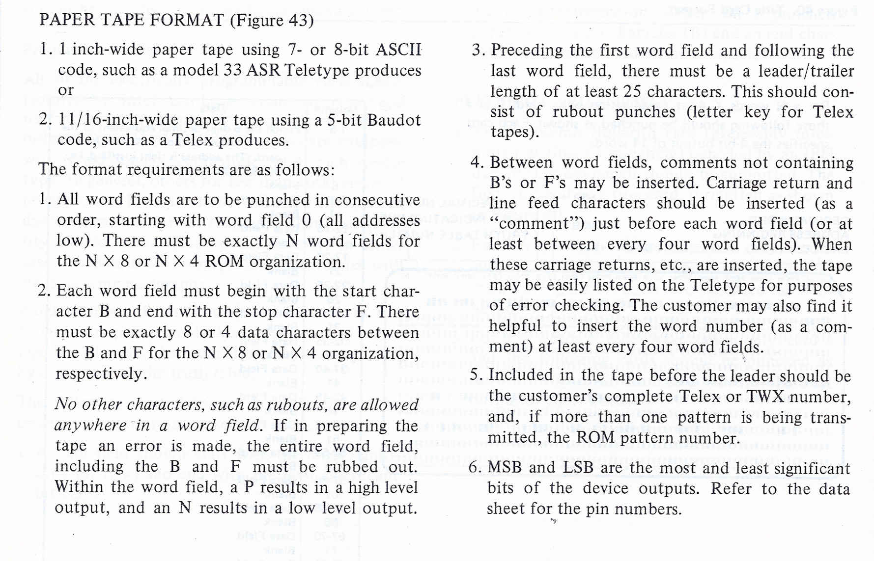
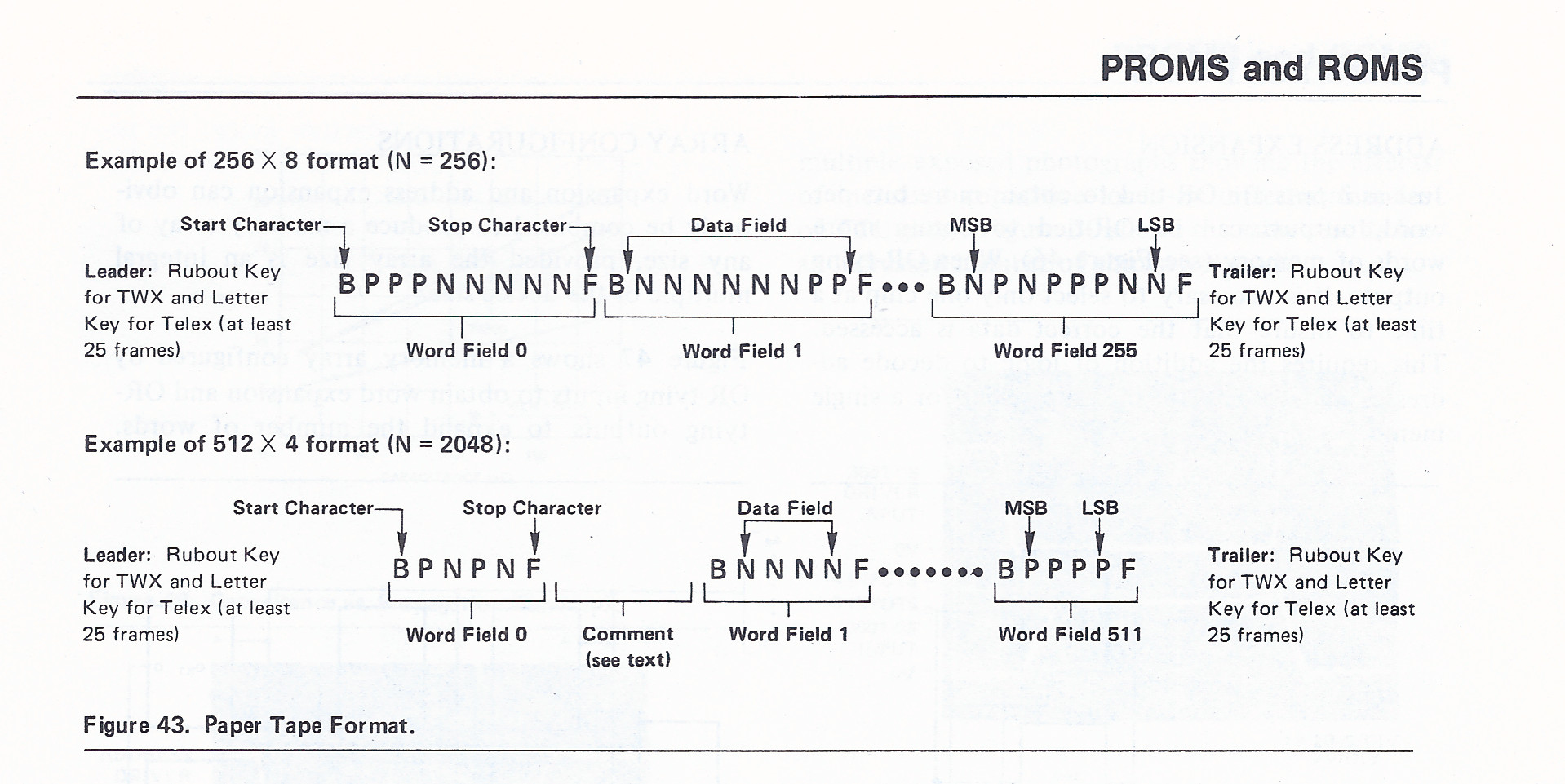
BNPF notation (Begin-Negative-Positive-Finish) is an old ASCII-based text file format created by Intel to specify memory contents and program PROMs and EPROMs.

BNPF (Begin-Negative-Positive-Finish), also written as BPNF (Begin-Positive-Negative-Finish).
In BNPF encoding, a single byte (8 bits) would be represented by a highly redundant character framing sequence starting with a single uppercase ASCII “B”, eight ASCII characters where a “0” would be represented by a “N” and a “1” would be represented by a “P”, followed by an ending ASCII “F”. These ten-character ASCII sequences were separated by one or more whitespace characters, therefore using at least eleven ASCII characters for each byte stored (9% efficiency). The ASCII “N” and “P” characters differed in four bit positions, providing excellent protection from single punch errors.

Structure of BNPF Format

  • Brackets: Every data word field begins with the letter B (Begin) and ends with F (Finish/Final).
  • Bit Values: Characters between B and F represent data bits using P (Positive) for high/1 or N (Negative) for low/0, ordered from most to least significant.
  • Don’t Care: An X character can be used inside the sequence to represent a wildcard or “don’t care” bit.
  • Repetition: The syntax BPNF allows a number N to repeat the previous word field multiple times.
  • Comments: Any text or comments outside of the B…F blocks (provided they do not contain the letters B or F) are ignored by the programmer

Example of BNPF output

.M  7000 85 F9 A9 23 D0 55 A9 16

85 = 10000101 
    BPNNNNPNPF 

.WB 7000 7100
7000 BPNNNNPNPF BPPPPPNNPF BPNPNPNNPF BNNPNNNPPF
     ^^^^^^^^^^
.WH 7000 7100
;18700085F9A923D055A9168D036EA208BDF7739DF7FFCAD0F786EA0F19
       ^^

More examples: notice the removal of the B character from the address. According to the specification, also the F character should be removed, but the routine responsible (ASCI in Write hex routines) only checks for B.

.WB B000 B100
 000 BNNNNNNNNF BNNNNNNNNF BNNNNNNNNF BNNNNNNNNF
 004 BNNNNNNNNF BNNNNNNNNF BNNNNNNNNF BNNNNNNNNF
 008 BNNNNNNNNF BNNNNNNNNF BNNNNNNNNF BNNNNNNNNF
 00C BNNNNNNNNF BNNNNNNNNF BNNNNNNNNF BNNNNNNNNF

.WB 70B0  7100
70 0 BNNNNNNPPF BNNPNNNNNF BNPPPNPNNF BNPPPNNPPF
.

Here the official definition of BNPF code from the Intel Memory Design handbook 1975, page 8-28 and 8-29.

0481   723B E6 FD       WB     INC SAVX          ; SAVX TO = NCMDS FOR ASCII SUB/R
0482   723D A5 E4       WB1    LDA WRAP          ;IF ADDR HAS WRAPPED AROUND
0483   723F D0 F7              BNE BCCST         ;THEN TERMINATE WRITE OPERATION
0484   7241             ;
0485   7241 A9 04              LDA #4
0486   7243 85 EC              STA ACMD
0487   7245 20 8A 72           JSR CRLF
0488   7248 20 9A 72           JSR WROA          ; OUTPUT HEX ADR
0489   724B             ;
0490   724B 20 77 73    WBNPF  JSR SPACE
0491   724E A2 09              LDX #9
0492   7250 86 FE              STX TMPC          ; LOOP CNT =9
0493   7252 A1 E5              LDA (TMP0-9,X)
0494   7254 85 FF              STA TMPC2         ; BYTE TO TMPC2
0495   7256 A9 42              LDA #'B'
0496   7258 D0 08              BNE WBF2          ; WRITE B
0497   725A             ;
0498   725A A9 50       WBF1   LDA #'P'
0499   725C 06 FF              ASL TMPC2
0500   725E B0 02              BCS WBF2
0501   7260 A9 4E              LDA #'N'
0502   7262             ;
0503   7262 20 C6 72    WBF2   JSR WROC          ; WRITE N OR P
0504   7265 C6 FE              DEC TMPC
0505   7267 D0 F1              BNE WBF1          ; LOOP
0506   7269 A9 46              LDA #'F'
0507   726B 20 C6 72           JSR WROC          ; WRITE F
0508   726E             ;
0509   726E 20 97 73           JSR INCTMP
0510   7271             ;
0511   7271 C6 EC              DEC ACMD          ; TEST FOR MULTIPLE OF FOUR
0512   7273 D0 D6              BNE WBNPF
0513   7275             ;
0514   7275 20 C1 70           JSR DCMP
0515   7278 B0 C3              BCS WB1           ; LOOP WHILE EA GT OR = SA
0516   727A 90 BC              BCC BCCST
0517   727C             ;
0518   727C 48          CADD   PHA               ; SAVE A
0519   727D 18                 CLC
0520   727E 65 F2              ADC TMP4
0521   7280 85 F2              STA TMP4
0522   7282 A5 F3              LDA TMP4+1
0523   7284 69 00              ADC #0
0524   7286 85 F3              STA TMP4+1
0525   7288 68                 PLA               ; RESTORE A
0526   7289 60                 RTS

0262   70C1 38          DCMP   SEC               ; TMP2-TMP0 DOUBLE SUBTRACT
0263   70C2 A5 F0              LDA TMP2
0264   70C4 E5 EE              SBC TMP0
0265   70C6 85 E5              STA DIFF
0266   70C8 A5 F1              LDA TMP2+1
0267   70CA E5 EF              SBC TMP0+1
0268   70CC A8                 TAY               ; RETURN HIGH ORDER PART IN Y
0269   70CD 05 E5              ORA DIFF          ; OR LO FOR EQU TEST
0270   70CF 60                 RTS

0478   7238 4C 86 70    BCCST  JMP START

What is happening here?
This routine is called from the W command handler if after the W the character B is typed by the user. So the command paraneters start and end addresa re already parsed
– start address in TMP0
– end address in TMP0+2

  • save this command in NCMDS for ASCI routine, called from WROB write byte as two hex characters (481)
  • loop address range
    • if address wrap around we rare finished, return to START (482-483)
    • ACMD = 4 to have four bytes per line (485-487)
    • loop ACMD 4 times
      • CRLF + print address via WROA, see hex routines (487-488)
        • print space
        • TMPC = 9 characters to print (491-492)
        • TMPC2 is byte to print as BNPF format
        • print B
        • loop TMPC
          • shift TMPC2 bit in to carry (499)
          • if carry set print P else print N (498-505)
        • print F (506)
      • next address (514)
  • jump to start (516, 478)

Note WROA calls ASCII, to perform the byte to ASCII conversion, There the command code in NCMDS is ued to suppress the B in the address, the address is considered to be a comment to the PROM programmer device.

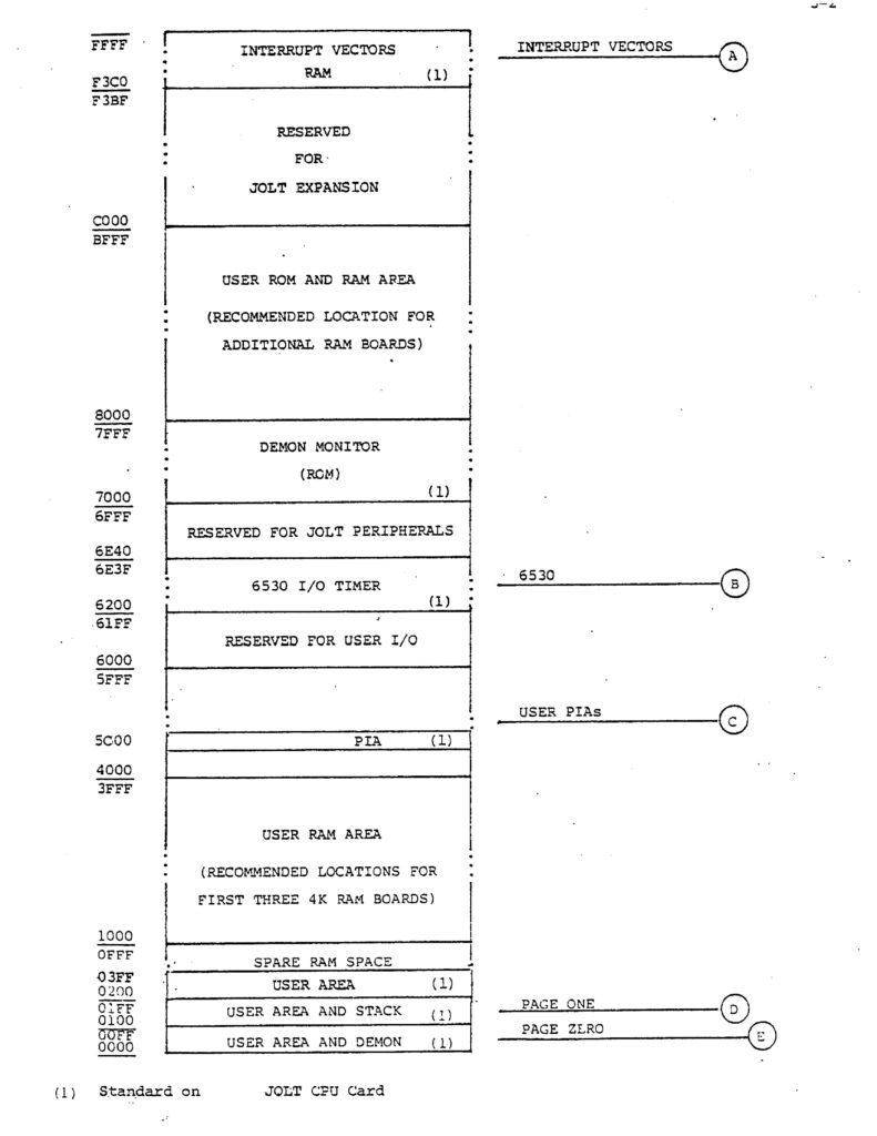
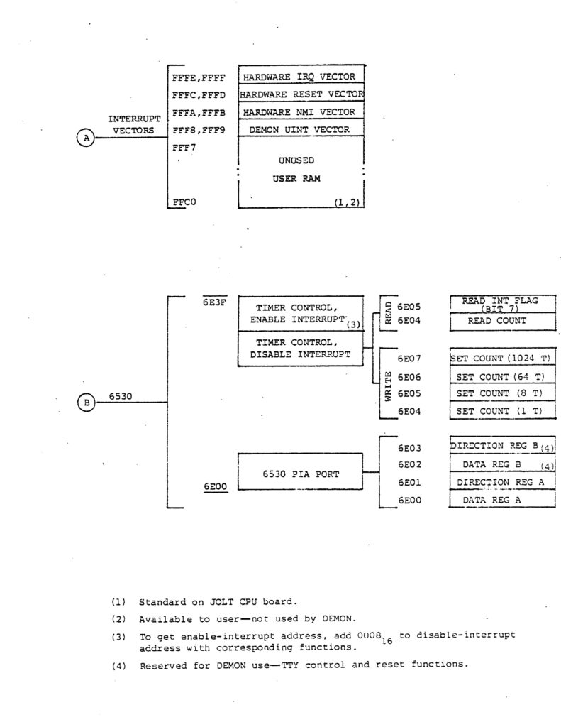
Memory map

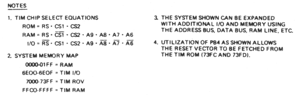
This is the memory map after RESET.

RESET of TIM

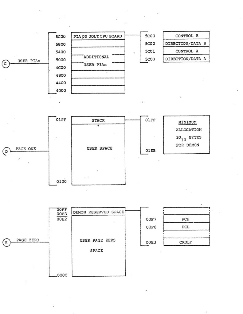
The RESET of a system with a 6530-004 TIM is a bit special. The RESET code comes from the OTIM ROM, after the RESET the memory map is restored to the documented one.

0084   0000             MDBK   =%00010110        ; X,X,X,PCR,DATA-AVAIL,GOT-DATA,SERIAL-OUT,IN

0095   0000             UINT   =$FFF8  

0793   73F8 00 70       INTVEC .WORD NMINT       ; DEFAULT USER INTRO TO NMINT
0794   73FA 00 70              .WORD NMINT
0795   73FC 06 70              .WORD RESET
0796   73FE 52 70              .WORD INTRQ
	
0144   7006 A9 16       RESET  LDA #MDBK         ; INIT DIR REG, PCR TO 1 RELOCATES
0145   7008             ;
0146   7008 8D 03 6E           STA MDB
0147   700B             ;
0148   700B A2 08              LDX #8            ; X=0
0149   700D BD F7 73    R1     LDA INTVEC-1,X    ; INITALIZE INT VECTORS
0150   7010 9D F7 FF           STA UINT-1,X
0151   7013 CA                 DEX
0152   7014 D0 F7              BNE R1
0153   7016             ;
0154   7016 86 EA              STX MAJORT        ; INIT MAJOR T COUNT TO ZERO
0155   7018 86 E7              STX HSPTR         ; CLEAR HSPTR FLAGS
0156   701A 86 E8              STX HSROP
0157   701C CA                 DEX               ; X=FF
0158   701D 9A                 TXS               ; SP=FF

The Chip Select equations for the 6530-004

What is happening here?

The address decoding is a bit course, the ROM of the 6530-004 is not only at $7000, but also mirrored at $7400, $7800 and $7C00. So $73FF is also $7FFF.

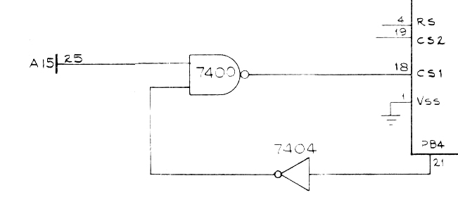
The PB4 circuit from the TIM manual


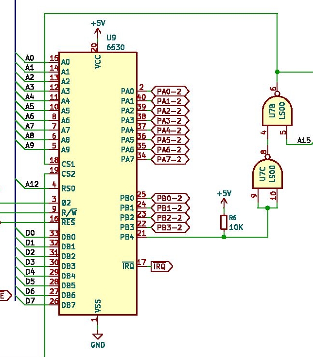
The PB4 circuit in the Jolt, note the pullup resistor.

After power PB4 is an input, the default for a 6530 port. So the inverter input is seen as high (on the Jolt a pullup resistor makes that certain) , so the output of the inverter is low. This blocks the 7400 port input, the other input is A15. So the ROM address $7FFF is mirrored to $FFFF. And so the RESET vector of the 6502 is read from the ROM the 6530-004, and the program counter is set to $7006, the RESET code in the ROM.

The Data Direction register or Port B is loaded with MDBK =%00010110

  • 0 PB0 input serial in
  • 1 PB1 output serial out
  • 1 PB2 is output GOT-Data High speed reader
  • 0 PB3 is input DAT-Avail High Speed reader
  • 1 PB4 is output PCR this makes PB4 low and A15 reaches the CS of the 6530-004.
  • 0 PB5 is input unused
  • 0 PB6 is input unused
  • 0 PB7 is input unused

By making PB4 an output, PB4 becomes low, the output of the 7400 high, and A15 reaches the 6530, so the ROM is not seen at FFFF. Teh default memory map is now active.

The 8 vector bytes from the ROM are now loaded into the RAM of the 6430-004 at upper memory (location UINT) in a loop with X as down counter to zero (148-152)

Some counters and flags are now initialized to zero with X (High speed reader, serial T count) (154 to 156)

As last the stack pointer is set to $FF (157-158)

JOLT TIM DEMON explained

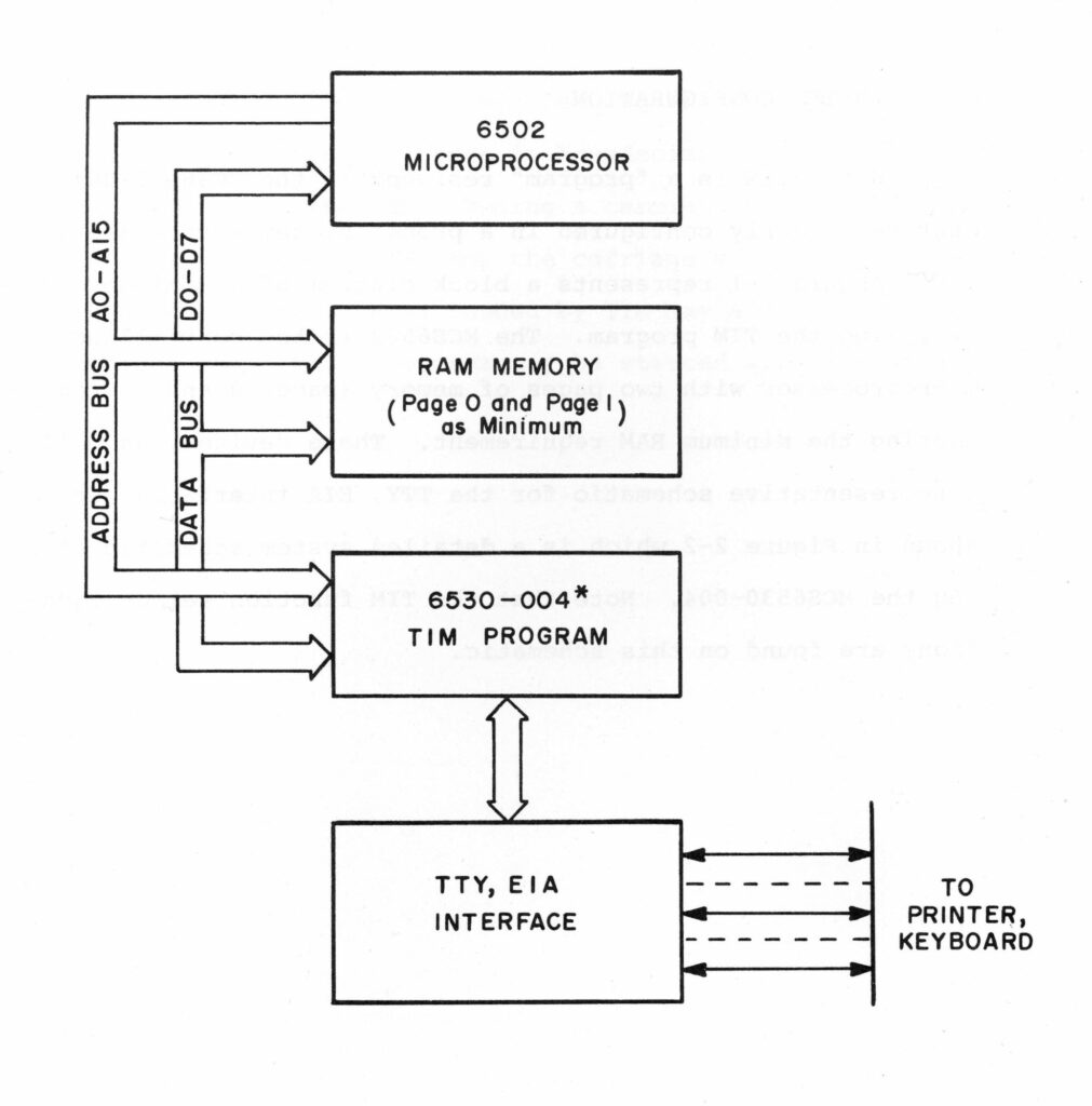
The Jolt and SuperJolt computers use the 6530-004 RRIOT TIM IC. The Jolt is in fact just a board with a 6502 with a TIM RRIOT + some RAM and a PIA 6520 and some decoding logic.
The program in the TIM is called DEMON by Micro Associates (Ray Holt and Manny Lemas).

So understanding how the Jolt works starts with understanding how the TIM RRIOT hard- and software works.

The TIM RRIOT, 6530-004,contains the ROM (1K), timers, 128 byte RAM, 16 I/O) and 64 bytes RAM.

TIM DeMon Manuals

MOS TIM folder with pricelist
MOS TIM manual Rev 6500-20
Jolt DeMon software manual, the same as TIM
(this manual has an alternative listing of the TIM 6530-004 monitor), only the first page is different.
Jolt Replica User manual

TIM sources

Here the machine readable and ready to assemble source, listing and binary  of TIM (Thanks Martin Hoffmann-Vetter)
Note that this contains a corrected version, version 2026! While testing the TIM Simulator I found an error in the papertape loader LH command, the ‘;’ start of a record seems to be OCR’ed to ‘:’ . In 2026, during the deep dive into explaining the TIM, many OCR errors in the comments were corrected.
The resulting binary is identical to the ROM dumped from a real 6530-004.
The source listing is used on the next pages to explain the software.

TIM/Jolt explained

Jolt replica

The 7427 and the white 6502 have arrived and are showing off in the time period correct Jolt replica.

Jolt replica with ‘time period correct’ old parts

Eduardo Casino has done a great job replicating the PCB of the Jolt. And he proved the PCB was OK by building a Jolt and setting it to work.

I have populated a replica PCB with as much as I have in my junk boxes ‘time period correct’ parts. It does look good compared to photos of the original Jolt.
I am waiting for a ‘white’ 6502 to arrive, the purple one is already period correct.
This Jolt is meant to be a ‘museum’ part and will end up above my desk next to an original SuperJolt.
The next Jolt I will build will be a functional one with ‘black’ ICs and less attention to perfection.