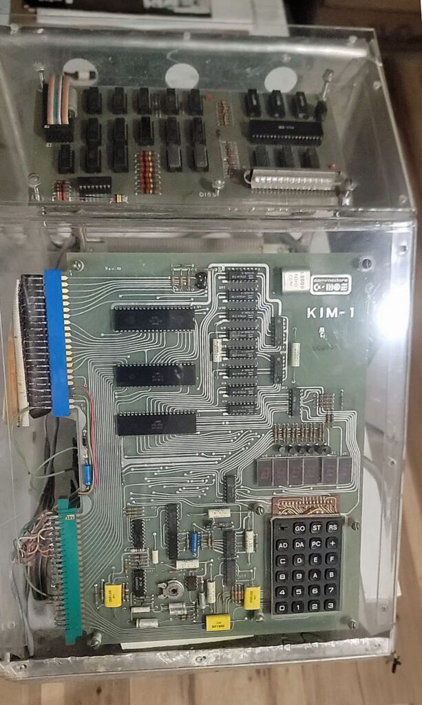
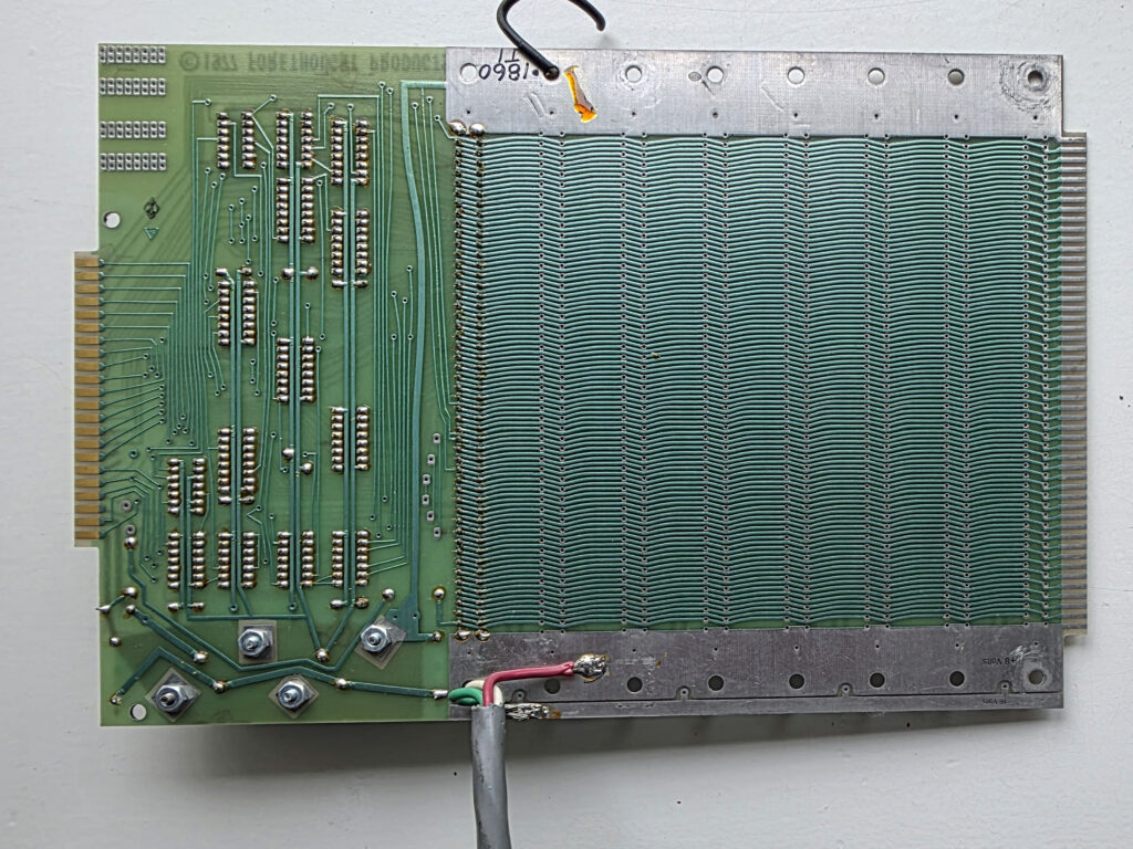
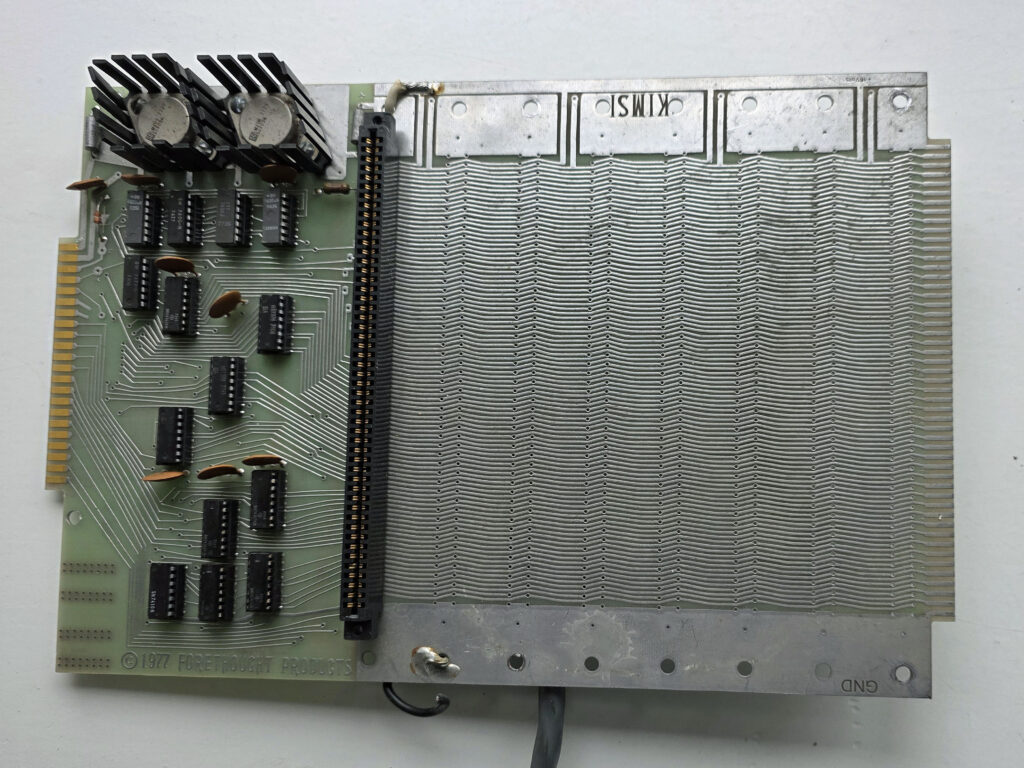
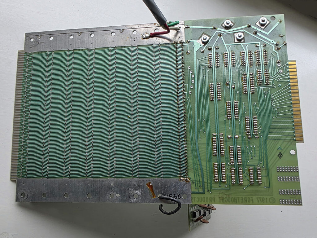
KIM-1 monitor data storage

The 6530-002 and 6530-003 software use these data areas:

0069 00EF .ORG $00EF
0070 00EF ; MPU REG. SAVX AREA IN PAGE 0

0071 00EF ;
0072 00EF PCL .BLOCK 1 ; PROGRAM CNT LOW
0073 00F0 PCH .BLOCK 1 ; PROGRAM CNT HI
0074 00F1 PREG .BLOCK 1 ; CURRENT STATUS REG.
0075 00F2 SPUSER .BLOCK 1 ; CURRENT STACK POINT
0076 00F3 ACC .BLOCK 1 ; ACCUMULATOR
0077 00F4 YREG .BLOCK 1 ; Y INDEX
0078 00F5 XREG .BLOCK 1 ; X INDEX
0079 00F6 ;
0080 00F6 ; KIM FIXED AREA IN PAGE 0
0081 00F6 ;
0082 00F6 CHKHI .BLOCK 1
0083 00F7 CHKSUM .BLOCK 1
0084 00F8 INL .BLOCK 1 ; INPUT BUFFER
0085 00F9 INH .BLOCK 1 ; INPUT BUFFER
0086 00FA POINTL .BLOCK 1 ; LSB OF OPEN CELL
0087 00FB POINTH .BLOCK 1 ; MSB OF OPEN CELL
0088 00FC TEMP .BLOCK 1
0089 00FD TMPX .BLOCK 1
0090 00FE CHAR .BLOCK 1
0091 00FF MODE .BLOCK 1
0092 0100 ;
0093 0100 ; KIM FIXED AREA IN PAGE 23 (in 6530-002 RAM)
0095 17E7 .ORG $17E7
0096 17E7 CHKL .BLOCK 1
0097 17E8 CHKH .BLOCK 1 ; CHKSUM
0098 17E9 SAVX .BLOCK 3
0099 17EC VEB .BLOCK 6 ; VOLATILE EXEC BLOCK (6-B)
0100 17F2 CNTL30 .BLOCK 1 ; TTY DELAY
0101 17F3 CNTH30 .BLOCK 1 ; TTY DELAY
0102 17F4 TIMH .BLOCK 1
0103 17F5 SAL .BLOCK 1 ; LOW STARTING ADDRESS
0104 17F6 SAH .BLOCK 1 ; HI STARTING ADDRESS
0105 17F7 EAL .BLOCK 1 ; LOW ENDING ADDRESS
0106 17F8 EAH .BLOCK 1 ; HI ENDING ADDRESS
0107 17F9 ID .BLOCK 1 ;
0108 17FA ;
0109 17FA ; INTERRUPT VECTORS
0110 17FA ;
0111 17FA NMIV .BLOCK 2 ; STOP VECTOR (STOP=1C00)
0112 17FC RSTV .BLOCK 2 ; RST VECTOR
0113 17FE IRQV .BLOCK 2 ; IRQ VECTOR (BRK=1C00)

Dump to tape

DUMPT dumps via bitbanging a KIM-1 audio tape file.

Very straight forward well commented source.
See also the user manual, which explains the technique quite well.

0119   1800             ;       DUMP MEMORY TO TAPE 
0120   1800               
0121   1800 A9 AD       DUMPT   LDA   #$AD         ; LOAD ABSOLUTE INST
0122   1802 8D EC 17            STA   VEB
0123   1805 20 32 19            JSR   INTVEB
0124   1808             ;             
0125   1808 A9 27               LDA   #$27         ; TURN OFF DATAIN PB5
0126   180A 8D 42 17            STA   SBD          
0127   180D A9 BF               LDA   #$BF         ; CONVERT PB7 TO OUTPUT
0128   180F 8D 43 17            STA   PBDD         
0129   1812             ;                          
0130   1812 A2 64               LDX   #$64         ; 100 CHARS
0131   1814 A9 16       DUMPT1 LDA    #$16         ; SYNC CHAR'S
0132   1816 20 7A 19            JSR   OUTCHT       
0133   1819 CA                  DEX                
0134   181A D0 F8               BNE   DUMPT1       
0135   181C             ;                         
0136   181C             
0137   181C A9 2A       	LDA   #$2A         ; START CHAR
0138   181E 20 7A 19            JSR   OUTCHT        
0139   1821             ;
0140   1821 AD F9 17            LDA   ID           ; OUTPUT ID
0141   1824 20 61 19            JSR   OUTBT         
0142   1827             ;
0143   1827 AD F5 17            LDA   SAL          ; OUTPUT STARTING
0144   182A 20 5E 19            JSR   OUTBTC       ; ADDRESS
0145   182D AD F6 17            LDA   SAH           
0146   1830 20 5E 19            JSR   OUTBTC        
0147   1833             ;
0148   1833 AD ED 17    DUMPT2  LDA   VEB+1        ; CHECK FOR LAST
0149   1836 CD F7 17            CMP   EAL          ; DATA BYTE
0150   1839 AD EE 17            LDA   VEB+2         
0151   183C ED F8 17            SBC   EAH           
0152   183F 90 24               BCC   DUMPT4        
0153   1841             ;
0154   1841 A9 2F               LDA   #'/'         ; OUTPUT END OF DATA CHAR
0155   1843 20 7A 19            JSR   OUTCHT        
0156   1846 AD E7 17            LDA   CHKL         ; LAST BYTE HAS BEEN
0157   1849 20 61 19            JSR   OUTBT        ; OUT PUT    NOW OUTPUT
0158   184C AD E8 17            LDA   CHKH         ; CHKSUM
0159   184F 20 61 19            JSR   OUTBT         
0160   1852             ;
0161   1852             ;
0162   1852 A2 02               LDX   #$02         ; 2 CHAR'S
0163   1854 A9 04       DUMPT3  LDA   #$04         ; EOT CHAR
0164   1856 20 7A 19            JSR   OUTCHT        
0165   1859 CA                  DEX                 
0166   185A D0 F8               BNE   DUMPT3   
0167   185C             		
0168   185C A9 00               LDA   #$00 ; DISPLAY 0000
0169   185E 85 FA               STA   POINTL       ; FOR NORMAL EXIT
0170   1860 85 FB               STA   POINTH        
0171   1862 4C 4F 1C            JMP   START         
0172   1865             ;
0173   1865 20 EC 17    DUMPT4  JSR   VEB          ; DATA BYTE OUTPUT
0174   1868 20 5E 19            JSR   OUTBTC  
0175   186B             ;		
0176   186B 20 EA 19            JSR   INCVEB
0177   186E 4C 33 18            JMP   DUMPT2

Audio tape hardware and ROM

The second RRIOT, named 6530-003, in the KIM-1 is nearly free to use by the user. The two parallel ports, the timer, the RAM, not used by the software.

But the ROM is used, it contains two routines to dump and load data on audio cassette tape. The hardware for this is connected to the 6530-002.

The hardware for audio out is simple, the software does all the work of producing audio tones at PB7, with some pulse shaping with a capacitor/resistor and a ‘low’
or ‘high’ amplitude output.

Audio in is a bit more complicated. The PLL LM565 Phase Locked Loop detects the frequency of incoming audio signals, the output of the PLL is converted to TTL level by the comparator LM311. This is is the only part of the KIM-1 hardware requiring 12V.
See here the datasheet of the LM565.

On pin7 a TTL signal is seen if there is a KIM-1 compatible audio signal is coming in.
Read Appendix E of the User manual to see how all this works.

The two routines, LOADT and DUMPT, are described on the next pages. The style of the programming is a different from the main ROM. It is better structured and easily readable.

Where the 6530-002 papertape routines use indexed zeropage addressing to load/save bytes in memory, the 6530-003 uses a so called Volatile Execution Block VEB in page 23.
A small routine is constructed there during the dump and load.

For DUMPT
AD yy xx 60 LDA xxyy RTS

for LOADT
8D yy xx 4C TAP STA xxyy XX JMP LOADT12

The address xxyy is incremented during the load or dump.

DUMPT and LOADT are completely independent of the monitor in the KIM 6530-002. So you have to start the routines via the GO command or key. The routines end with a call to START in the main routine, where an error condition is indicated with the current address: 0000 is succes, FFFF is error.

It would have been nice to integrate DUMPT and LOADT with command in the TTY loop for example and return via the normal exit routine, displaying ERR KIM as the papertape routines do.
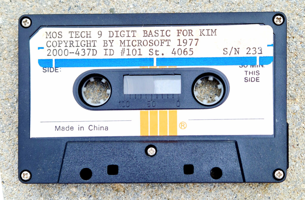
Also making it callable as subroutine might have nice for programs like the KB9 MOS Technology Basic for the KIM or Focal instead of falling back to the KIM monitor.

Expanding the KIM-1

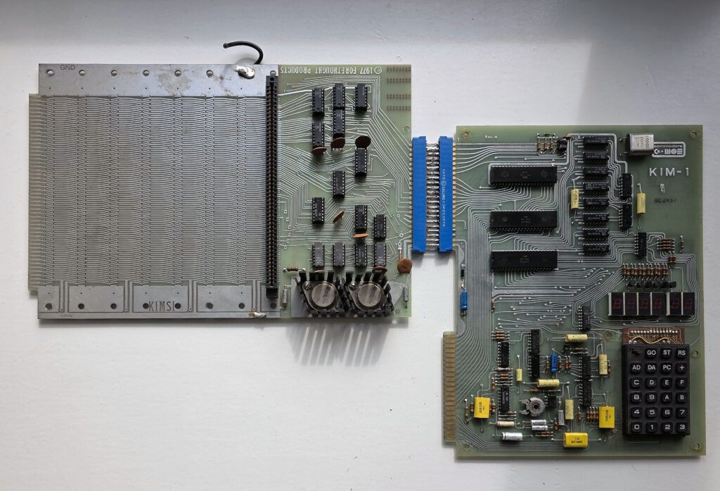
On the page KIM-1 Memory layout you can see the KIM-1 in its basic form of address decoding is limited to 8K address space, repeated 8 times in the 64K address space.
So the KIM-1 can boot from the KIM-1 ROM since address 17FA is the same as FFFA.

The basic memory decoder in the KIM-1

Simple expansion
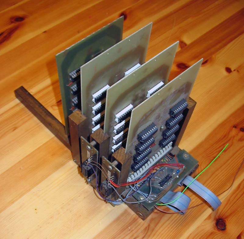
A first memory expansion often used in the KIM-1 is to use K1, K2, K3 and K4. When you place RAM there, location 0400-13FF become available. The KIM-1 still sees 8K repeated in the 64K
My first expansion was made this way, four 1K SRAM cards made 4K RAM extra available. Great for Tiny Basic.
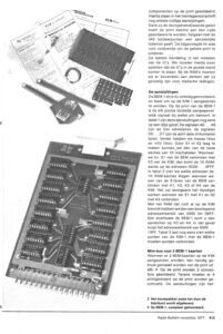
This is described in the Radio Bulletin article with the 1K B.E.M. static RAM card.

Chapter 6 of the User manual has good advice on the memory decoding.

If we want to expand the access of the 6502 to more than *K , we need to involve address lines A13, A14 and A15 and use DECODE ENABLE to limit K0-K7 to the first 8K of the address space..

This was my second expansion, as described in this article.
With 4K RAM cards, 2114 SRAM based.

You see here A13, A14, A15 connected to a 74145 used as 3 to 8 decoder. Again the 74145 is used for its open collector outputs.
This delivers signals 8K0 to 8K7, where 8K0 selects 0000-1FFF, 8K1 2000-3FFF and so on, 8K7 selects E000-EFFF.
By tying signal 8K0 to 8K7 we repeat 0000-1FFF to E000-FFFF and the KIM-1 ROM vector is mapped in for a RESET. So we gain access to 2000-DFFF for expansion.
The second and third 74145 is an example to deliver Kx signals for 4KB memory parts. I added 32K SRAM this way with 8 4K RAM cards.

If you want access to address space E000-FFFF, you have to provide ROM at FFFA-FFFF, or map this address space to 17FA-17FF.

The same principles are used in the Micro-KIM and PAL-1 RAM card. and the PAL-2 full decode.

PAL-1 and Micro-KIM RAM board

PAL-2 decoder

KIM-1 memory layout

The 6502 has an 16 bit address bus, so it can access 64KB of memory, made up of RAM, ROM and I/O devices.
Address decoding is the hardware that enables the devices in that memory space at the desired address.

The basic address decoding is made up of a 74145, a TTL IC that decodes 4 bit to 10 bits, here used as 3 to 8 decoder. Te 74145 has open collector outputs, so outputs can be tied together.

74145 function table

Memory decoder in the KIM-1

According the User manual this leads to the memory layout as shown above. Note the K0-K7 signals that are connected to the hardware devices such a RAM, and the RRIOTs.
The Kx signal covers a 1KB block of memory, a ‘Page’ is 256 bytes, 4 pages in a Kx block. So K0 addresses pages 0..3, K5 has page 23 which you will see mentioned in the source as the RAM locations in use by the monitor.

Incomplete memory decoding
The picture from the user manual above is a bit misleading. Since address A13, A14 and A15 are not included in the decoder, they are effectively ignored. The KIM-1 sees a maximum of 8K memory this way 0000-1FFF. Why still using 16 bit addresses? In fact since the higher address lines are ignored, address 0000 is also address 2000, 4000 etc with 8K steps to E000.
And the vectors at address 1FFA in the KIM ROM are also found at FFFA, so the RESET vector works. Simple and effective.
The KIM-1 in its basic form of address decoding is limited to 8K address space, repeated 8 times in the 64K address space.

DE Decode enable
The fourth input D of the 74145 is connected to pin A-K of the Application connector. For the basic address decoding as 3 to 8 decoder pin D of the 74145 has to be connected to ground.
This is the essential wire on the Application connector to let a KIM-1 function.
DE is essential for external devices to take over the 6502 address space and allow expansion utilizing the full address space.

Conclusion
The KIM-1 has access to a 8K memory space. Any address is truncated to 13 bits in hardware, so if you use an address 2000 and up it is mapped into 0000-1FFF.

Further reading
Chapter 6 of the User manual has good advice on the memory decoding.

On the next page, Expand the KIM-1, you will see how to add RAM, ROM and I/O to the KIM-1 and use the full address space, with full decode and using Decode Enable.

LED Display and keyboard

Routines to light LED display and checking for a key pressed by multiplexing the seven segment LED and checking if a key is pressed. Must be called in a loop, since the lighting is only for a short time.

This complex looking circuit is the magic that makes the LED Display and keyboard work.

Actually this is made up of two circuits: the multiplexed LED display and the keyboard matrix.

The multiplexed LED display

By multiplexing the lighting of the seven segment LED displays not much special hardware is required to have a hex keypad and 6 digit serviced.
All LED displays have the segment inputs connected to each other and Port A PA0-PA6 as output are connected to the led segments a-g, PA0 = a .. PA6 = g.
The 74145 outputs O4..)9 are connected to the cathodes of the corresponding LED display.
So by setting the PB1..PB4 inputs of the 74145 one LED display is lighted, the others are off. By lighting this for a small delay and then stepping to the next display all LEDs are lighted after each other. If this is done fast enough the slow human eyes will not see this as a flickering light.
This is what is happening in the SCAND(1) routine.


Reading the keyboard matrix

The keyboard matrix is also read out by multiplexing rows and columns checking for a short circuit if a key is pressed, via
PA0..6 as inputs and the outputs of the 74145 00-03.
By selecting row 0 to 3 (output 00 to 03 of the 74145) and reading PA0 to PA6 a pressed key is detected.
In the GETKEY routine a key is detected this way, debounced and converted to a key number 00.14.

PB1-4 to 74145 decoder

The 74145 serves the multiplexing. From the RRIOT Port B PB1 .. PB4 to A..D inputs decodes to 10 outputs 00..09.
00 – 03 Keyboard KB Row 0-3
04 – O9 outputs switch LED display 1..6 on/off one by one.
Also available on the Application connector!

Part of the keypad is the TTY/KB switch, connected via Application connector 21-V = PA0 to O3 KB Row 3 connected via switch/jumper

1030   1EFE             ;
1031   1EFE             ;       SUB TO DETERMINE IF KEY IS 
1032   1EFE             ;       DEPRESSED OR CONDITION OF SSW 
1033   1EFE             ;            KEY NOT DEP OR TTY MODE     A=0
1034   1EFE             ;            KEY DEP OR KB MODE      A NOT ZERO
1035   1EFE             ;
1036   1EFE             ;
1037   1EFE A0 03       AK      LDY   #$03       ;  3 ROWS
1038   1F00 A2 01               LDX   #$01       ; DIGIT 0
1039   1F02             ;
1040   1F02 A9 FF       ONEKEY  LDA   #$FF
1041   1F04 8E 42 17    AK1     STX   SBD        ;  OUTPUT DIGIT
1042   1F07 E8                  INX              ;  GET NEXT DIGIT
1043   1F08 E8                  INX   
1044   1F09 2D 40 17            AND   SAD        ; INPUT SEGMENTS
1045   1F0C 88                  DEY   
1046   1F0D D0 F5               BNE   AK1
1047   1F0F                     
1048   1F0F A0 07               LDY   #$07
1049   1F11 8C 42 17            STY   SBD
1050   1F14             ;
1051   1F14 09 80               ORA   #$80
1052   1F16 49 FF               EOR   #$FF
1053   1F18 60                  RTS  

What is happening here?

  • Three rows, start with first digit 0 (1037-1040)
    • Select digit by setting 74145 to O(X) via PB1-4 (1041)
    • Check if key pressed, A <> 0 (1044)
    • next row until all rows done (1045-1046
  • restore default PB1 and PB2 1, PB3, PB4 0: Os low
  • return
    A=0 if key not depressed or TTY mode
    A<>0 if key depressed or KB mod

SCAND
show digits for a short time form current cell address and contents

1054   1F19             ;		
1055   1F19             ;       SUB OUTPUT TO 7-SEGMENT DISPLAY **
1056   1F19             ;
1057   1F19 A0 00       SCAND   LDY   #$00       ; GET DATA SPECIFIED 
1058   1F1B B1 FA               LDA   (POINTL),Y ; BY POINT
1059   1F1D 85 F9               STA   INH        ; SET UP DISPLAY BUFFER
1060   1F1F A9 7F               LDA   #$7F       ; CHANGE SEG
1061   1F21 8D 41 17            STA   PADD       ; TO OUTPUT
1062   1F24             ;		
1063   1F24 A2 09               LDX   #$09       ; INIT DIGIT NUMBER
1064   1F26 A0 03               LDY   #$03       ; OUTPUT 3 BYTES
1065   1F28             ;
1066   1F28 B9 F8 00    SCAND1  LDA   INL,Y      ; GET BYTE
1067   1F2B 4A                  LSR   A          ; GET MSD
1068   1F2C 4A                  LSR   A
1069   1F2D 4A                  LSR   A
1070   1F2E 4A                  LSR   A
1071   1F2F 20 48 1F            JSR   CONVD      ; OUTPUT CHAR
1072   1F32 B9 F8 00            LDA   INL,Y      ; GET BYTE AGAIN
1073   1F35 29 0F               AND   #$0F       ; GET LSD
1074   1F37 20 48 1F            JSR   CONVD      ; OUTPUT CHAR
1075   1F3A 88                  DEY              ; SET UP FOR NEXT BYTE
1076   1F3B D0 EB               BNE   SCAND1
1077   1F3D 8E 42 17            STX   SBD        ; ALL DIGITS OFF
1078   1F40 A9 00               LDA   #$00       ; CHANGE SEGMENT
1079   1F42 8D 41 17            STA   PADD       ; TO INPUTS
1080   1F45 4C FE 1E            JMP   AK         ; GET ANY KEY

SCAND display four digits of address and two digits of content.
3 bytes from F9..FA are converted to hex on the six digits.

What is happening here?

  • load current cell FA, FB to display buffer INH (1057..1058)
  • X = 9 is selection of digit number PB1..PB4 (04..09 of 74145)
  • Y = 3, number of bytes
    • load low part of byte (1066..1070)
    • display via CONVD (1071)
    • load high part of bye
    • display via CONVD (1074)
    • do next byte (1075..1076)
  • set all displays off PB1..PB4= 0 (1077)
  • PA0..PA6 to inputs (1078..1079)
  • return via AK (1080)

CONVD
Lights segment of current select digit for a short time.
Segments output via PA0..PA6.
Hex to segment conversion via TABLE lookup
Digit value in Y
X is digit number in PB1..PB4 format

1081   1F48             ; 		
1082   1F48             ;       CONVERT AND DISPLAY HEX 
1083   1F48             ;       USED BY SCAND ONLY
1084   1F48             ;
1085   1F48 84 FC       CONVD   STY   TEMP       ; SAVE Y
1086   1F4A A8                  TAY              ; USE CHAR AS INDEX
1087   1F4B B9 E7 1F            LDA   TABLE,Y    ; LOOKUP CONVERSION
1088   1F4E A0 00               LDY   #$00       ; TURN OFF SEGMENTS
1089   1F50 8C 40 17            STY   SAD       
1090   1F53 8E 42 17            STX   SBD        ; OUTPUT DIGIT ENABLE
1091   1F56 8D 40 17            STA   SAD        ; OUT PUT SEGMENTS
1092   1F59             		
1093   1F59 A0 7F               LDY   #$7F       ; DELAY 500 CYCLES APPROX.
1094   1F5B 88          CONVD1  DEY  
1095   1F5C D0 FD               BNE   CONVD1
1096   1F5E             	;
1097   1F5E E8                  INX              ; GET NEXT DIGIT NUM
1098   1F5F E8                  INX              ; ADD 2
1099   1F60 A4 FC               LDY TEMP  ; RESTORE Y
1100   1F62 60                  RTS

What is happening here?

  • convert hex to segment via TABLE lookup (1086 .. 1087)
  • turn off all segments PA0..PA6 (1088..1089)
  • enable digit via SBD = X (1090)
  • light segment via SAD = A, keep PA7 to 1 (1091)
  • delay some time (1093..1095
  • X = next display 2 hex per hex byte (1097)

[/code]

GETKEY
Get key pressed:
– Key pressed: A is key number
– No key: A = 15

Key values are:
0..9 = $00 ..$09
AD = $10 address mode
DA = $11 data mode
+ = $12 step
GO = $13 GO execute
PC = $14 PC mode

1108   1F6A             ;
1109   1F6A             ;       GET KEY FROM KEY BOARD 
1110   1F6A             ;       RETURN WITH A=KEY VALUE
1111   1F6A             ;       A GT. 15 TEHN ILLEGAL OR NO KEY
1112   1F6A             ;
1113   1F6A             ;
1114   1F6A A2 21       GETKEY  LDX   #$21       ; START AT DIGIT 0 
1115   1F6C A0 01       GETKE5  LDY   #$01       ; GET 1 ROW
1116   1F6E 20 02 1F            JSR   ONEKEY
1117   1F71 D0 07               BNE   KEYIN      ; A=0 NO KEY
1118   1F73 E0 27               CPX   #$27       ; TEST FOR DIGIT 2
1119   1F75 D0 F5               BNE   GETKE5
1120   1F77 A9 15               LDA   #$15       ; 15=NOKEY
1121   1F79 60                  RTS   

; key pressed

1122   1F7A A0 FF       KEYIN   LDY   #$FF
1123   1F7C 0A          KEYIN1  ASL   A          ; SHIFT LEFT
1124   1F7D B0 03               BCS   KEYIN2     ; UNTIL Y=KEY NUM
1125   1F7F C8                  INY   
1126   1F80 10 FA               BPL   KEYIN1
1127   1F82 8A          KEYIN2  TXA   
1128   1F83 29 0F               AND   #$0F       ; MASK MSD
1129   1F85 4A                  LSR   A          ; DIVIDE BY 2
1130   1F86 AA                  TAX   
1131   1F87 98                  TYA   
1132   1F88 10 03               BPL   KEYIN4
1133   1F8A 18          KEYIN3  CLC   
1134   1F8B 69 07               ADC   #$07       ; MULT (X-1) TIMES A
1135   1F8D CA          KEYIN4  DEX   
1136   1F8E D0 FA               BNE   KEYIN3
1137   1F90 60                  RTS
1138   1F91             ;

What is happening here?

  • check if key pressed (1114..1119)
  • return with $15 if none (1120)
  • calculate key number 00..14 from position in matrix (1122..1136)

TABLE
HEX to 7 segment lookup table, HEX number 0..F to segment a..g

bit 0 = a
bit 1 = b
bit 2 = c
bit 3 = d
bit 4 = e
bit 5 = f
bit 6 = g
bit 7 = 1 to keep PA7, the TTY output to 1

Seven segment layout
   a              
  ---
f| g  | b
  ---
e|    | c
  ---
   d

Examples
hex 0 is all 1 except g:    1011 1111 = $BF
hex A is all 1 except d:    1111 0111 = $F7
hex F is all 1 except b,c,d 1111 0001 = $F1
1200   1FE7             ;       TABLE HEX TO 7 SEGMENT
1201   1FE7             ;              0   1   2   3   4   5   6   7  
1202   1FE7 BF 86 DB CF TABLE   .BYTE  $BF,$86,$DB,$CF,$E6,$ED,$FD,$87
1202   1FEB E6 ED FD 87 
1203   1FEF             ;              8   9   A   B   C   D   E   F   
1204   1FEF FF EF F7 FC         .BYTE  $FF,$EF,$F7,$FC,$B9,$DE,$F9,$F1
1204   1FF3 B9 DE F9 F1 
1205   1FF7             ;

The following two pages from the First Book of KIM are also interesting to see what is happening here and how to expand the routine with a larger amount of characters to show on the display.


Main LED display and keyboard

Command execution from hex keyboard

0654   1C77             ;       MAIN ROTINE FOR KEY BOARD 
0655   1C77             ;       AND DISPLAY   
0656   1C77             ;
0657   1C77 20 19 1F    TTYKB   JSR   SCAND      ; IF A=0 NO KEY 
0658   1C7A D0 D3               BNE   START
0659   1C7C A9 01       TTYKB1  LDA   #$01
0660   1C7E 2C 40 17            BIT   SAD
0661   1C81 F0 CC               BEQ   START
0662   1C83 20 19 1F            JSR   SCAND
0663   1C86 F0 F4               BEQ   TTYKB1
0664   1C88 20 19 1F            JSR   SCAND
0665   1C8B F0 EF               BEQ   TTYKB1
0666   1C8D             ;		      
0667   1C8D 20 6A 1F            JSR   GETKEY
0668   1C90 C9 15               CMP   #$15
0669   1C92 10 BB               BPL   START
0670   1C94 C9 14               CMP   #$14
0671   1C96 F0 44               BEQ   PCCMD      ; DISPLAY PC
0672   1C98 C9 10               CMP   #$10       ; ADDR MODE=1
0673   1C9A F0 2C               BEQ   ADDRM
0674   1C9C C9 11               CMP   #$11       ; DATA MODE=1
0675   1C9E F0 2C               BEQ   DATAM
0676   1CA0 C9 12               CMP   #$12       ; STEP
0677   1CA2 F0 2F               BEQ   STEP
0678   1CA4 C9 13               CMP   #$13       ; RUN
0679   1CA6 F0 31               BEQ   GOV
0680   1CA8 0A                  ASL   A          ; SHIFT CHAR INTO HIGH
0681   1CA9 0A                  ASL   A          ; ORDER NIBBLE
0682   1CAA 0A                  ASL   A
0683   1CAB 0A                  ASL   A
0684   1CAC 85 FC               STA   TEMP       ; STORE IN TEMP
0685   1CAE A2 04               LDX   #$04
0686   1CB0 A4 FF       DATA1   LDY   MODE       ; TEST MODE 1=ADDR
0687   1CB2 D0 0A               BNE   ADDR       ; MODE=0 DATA
0688   1CB4 B1 FA               LDA  (POINTL),Y  ; GET DATA       
0689   1CB6 06 FC               ASL   TEMP       ; SHIFT CHAR
0690   1CB8 2A                  ROL   A          ; SHIFT DATA
0691   1CB9 91 FA               STA   (POINTL),Y ; STORE OUT DATA
0692   1CBB 4C C3 1C            JMP   DATA2
0693   1CBE             ;            
0694   1CBE 0A          ADDR    ASL   A          ; SHIFT CHAR
0695   1CBF 26 FA               ROL   POINTL     ; SHIFT ADDR
0696   1CC1 26 FB               ROL   POINTH     ; SHIFT ADDR HI
0697   1CC3 CA          DATA2   DEX  
0698   1CC4 D0 EA               BNE   DATA1      ; DO 4 TIMES
0699   1CC6 F0 08               BEQ   DATAM2     ; EXIT HERE
0700   1CC8             ;		
0701   1CC8 A9 01       ADDRM   LDA   #$01
0702   1CCA D0 02               BNE   DATAM1
0703   1CCC             ;
0704   1CCC A9 00       DATAM   LDA   #$00
0705   1CCE 85 FF       DATAM1  STA   MODE
0706   1CD0 4C 4F 1C    DATAM2  JMP   START
0707   1CD3             ;            
0708   1CD3 20 63 1F    STEP    JSR   INCPT                              
0709   1CD6 4C 4F 1C            JMP   START
0710   1CD9             ;
0711   1CD9 4C C8 1D    GOV     JMP   GOEXEC                              
0712   1CDC             ;
0713   1CDC             ;
0714   1CDC             ;       DISPLAY PC BY MOVING 
0715   1CDC             ;       PC TO POINT   
0716   1CDC             ;
0717   1CDC A5 EF       PCCMD   LDA   PCL                                 
0718   1CDE 85 FA               STA   POINTL
0719   1CE0 A5 F0               LDA   PCH
0720   1CE2 85 FB               STA   POINTH
0721   1CE4 4C 4F 1C            JMP   START

0714   1CDC             ;       DISPLAY PC BY MOVING 
0715   1CDC             ;       PC TO POINT   
0716   1CDC             ;
0717   1CDC A5 EF       PCCMD   LDA   PCL                                 
0718   1CDE 85 FA               STA   POINTL
0719   1CE0 A5 F0               LDA   PCH
0720   1CE2 85 FB               STA   POINTH
0721   1CE4 4C 4F 1C            JMP   START

What is happening here?

    check if TTY and light display (657 .. 665)
    get key

      key 15 and above exit 667..669)
      key 14 do display PC with PCCMD, move PC into current address (670..671, 717 721))
      key 13 do GOV jump GOEXEC
      key 12 do STEP, increment current address (708)
      key 11 do mode data (680-721)
      key 10 do mode address (680-721)
      key 0..9 shift key into display from right and update current cell

Save to papertape format

The TTY command Q dumps a MOS Technology papertape format to the console.

This requires setting up the end address at 17F7 and 17F8 and selecting the startadres as the current address (POINTL, POINH).

Note that the record count is always $18, so the dump continues beyond the end address specified!

Example run

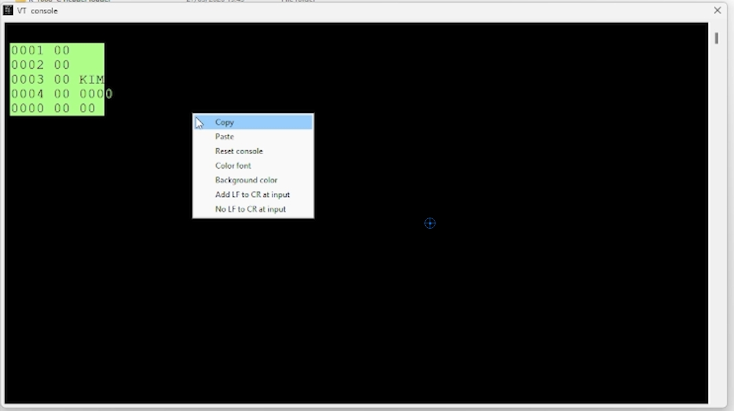
KIM
0000 00 17F7
17F7 00 FF.
17F8 00 02.
17F9 00 200
0200 00 Q
;180200000000000000000000000000000000000000000000000000001A
;1802180000000000000000000000000000000000000000000000000032
;180230000000000000000000000000000000000000000000000000004A
;1802480000000000000000000000000000000000000000000000000062
;180260000000000000000000000000000000000000000000000000007A
;1802780000000000000000000000000000000000000000000000000092
;18029000000000000000000000000000000000000000000000000000AA
;1802A800000000000000000000000000000000000000000000000000C2
;1802C000000000000000000000000000000000000000000000000000DA
;1802D800000000000000000000000000000000000000000000000000F2
;1802F0000000000000000000000000000000000000000000000000010A
;00000B000B
0000 00

The papertape format i described on the Load papertape format.

0866   1DF3 C9 51               CMP   #&#039;Q&#039;       ; DUMP FROM OPEN CELL TO HI LIMIT
0867   1DF5 F0 0A               BEQ   DUMPV

0873   1E01 4C 42 1D    DUMPV   JMP   DUMP


0778   1D42 A9 00       DUMP    LDA   #$00                                
0779   1D44 85 F8               STA   INL
0780   1D46 85 F9               STA   INH        ; CLEAR RECORD COUNT
0781   1D48 A9 00       DUMP0   LDA   #$00
0782   1D4A 85 F6               STA   CHKHI      ; CLEAR CHKSUM
0783   1D4C 85 F7               STA   CHKSUM
0784   1D4E             ;
0785   1D4E 20 2F 1E            JSR   CRLF       ; PRINT CR LF
0786   1D51 A9 3B               LDA   #$3B       ;  PRINT SEMICOLON
0787   1D53 20 A0 1E            JSR   OUTCH
0788   1D56 A5 FA               LDA   POINTL     ; TEST POINT GT OR ET
0789   1D58 CD F7 17            CMP   EAL        ;  HI LIMIT GOTO EXIT
0790   1D5B A5 FB               LDA   POINTH
0791   1D5D ED F8 17            SBC   EAH
0792   1D60 90 18               BCC DUMP4
0793   1D62             ;		
0794   1D62 A9 00               LDA   #$00       ;  PRINT LAST RECORD
0795   1D64 20 3B 1E            JSR   PRTBYT     ; 0 BYTES
0796   1D67 20 CC 1F            JSR   OPEN
0797   1D6A 20 1E 1E            JSR   PRTPNT
0798   1D6D             ;
0799   1D6D A5 F6               LDA   CHKHI      ; PRINT CHKSUM
0800   1D6F 20 3B 1E            JSR   PRTBYT     ; FOR LAST RECORD
0801   1D72 A5 F7               LDA   CHKSUM
0802   1D74 20 3B 1E            JSR   PRTBYT
0803   1D77 4C 64 1C            JMP   CLEAR
0804   1D7A             ;             
0805   1D7A A9 18       DUMP4   LDA   #$18       ; PRINT 24 BYTE COUNT 
0806   1D7C AA                  TAX              ; SAVE AS INDEX
0807   1D7D 20 3B 1E            JSR   PRTBYT
0808   1D80 20 91 1F            JSR   CHK
0809   1D83 20 1E 1E            JSR   PRTPNT
0810   1D86             ;		
0811   1D86 A0 00       DUMP2   LDY   #$00       ; PRINT 24 BYTES
0812   1D88 B1 FA               LDA   (POINTL),Y ; GET DATA
0813   1D8A 20 3B 1E            JSR   PRTBYT     ; PRINT DATA
0814   1D8D 20 91 1F            JSR   CHK        ; COMP CHKSUM
0815   1D90 20 63 1F            JSR   INCPT      ; INCREMENT POINT
0816   1D93 CA                  DEX   
0817   1D94 D0 F0               BNE   DUMP2
0818   1D96             ;
0819   1D96 A5 F6               LDA   CHKHI      ; PRINT CHKSUM
0820   1D98 20 3B 1E            JSR   PRTBYT
0821   1D9B A5 F7               LDA   CHKSUM
0822   1D9D 20 3B 1E            JSR   PRTBYT
0823   1DA0 E6 F8               INC   INL        ; INCR RECORD CNT
0824   1DA2 D0 02               BNE   DUMP3
0825   1DA4 E6 F9               INC   INH
0826   1DA6 4C 48 1D    DUMP3   JMP   DUMP0

1184   1FCC             ;
1185   1FCC A5 F8       OPEN    LDA   INL        ; MOVE I/O BUFFER TO POINT
1186   1FCE 85 FA               STA   POINTL
1187   1FD0 A5 F9               LDA   INH        ; TRANSFER INH- POINTH
1188   1FD2 85 FB       	STA   POINTH
1189   1FD4 60          	RTS   

0917   1E3B 85 FC       PRTBYT  STA   TEMP                             
0918   1E3D 4A                  LSR   A           ; SHIFT CHAR RIGHT 4 BITS
0919   1E3E 4A                  LSR   A
0920   1E3F 4A                  LSR   A
0921   1E40 4A                  LSR   A
0922   1E41 20 4C 1E            JSR   HEXTA       ; CONVERT TO HEX AND PRINT
0923   1E44 A5 FC               LDA   TEMP        ; GET OTHER HALF
0924   1E46 20 4C 1E            JSR   HEXTA       ; CONVERT TO HEX AND PRINT
0925   1E49 A5 FC               LDA   TEMP        ; RESTORE BYTE IN A AND RETURN
0926   1E4B 60                  RTS   
0927   1E4C             ;
0928   1E4C 29 0F       HEXTA   AND   #$0F        ; MASK HI 4 BITS
0929   1E4E C9 0A               CMP   #$0A
0930   1E50 18                  CLC   
0931   1E51 30 02               BMI   HEXTA1
0932   1E53 69 07               ADC   #$07        ; ALPHA HEX
0933   1E55 69 30       HEXTA1  ADC   #$30        ; DEC HEX
0934   1E57 4C A0 1E            JMP   OUTCH       ; PRINT CHAR

1139   1F91             ;       SUB TO COMPUTE CHECKSUM 
1140   1F91             ;
1141   1F91 18          CHK     CLC
1142   1F92 65 F7               ADC   CHKSUM
1143   1F94 85 F7               STA   CHKSUM
1144   1F96 A5 F6               LDA   CHKHI
1145   1F98 69 00               ADC   #$00
1146   1F9A 85 F6               STA   CHKHI
1147   1F9C 60                  RTS

0895   1E1E             ;       SUB TO PRINT POINTL,POINTH
0896   1E1E             ;
0897   1E1E A5 FB       PRTPNT  LDA   POINTH     ; PRINT POINTL, POINTH 
0898   1E20 20 3B 1E            JSR   PRTBYT
0899   1E23 20 91 1F            JSR   CHK
0900   1E26 A5 FA               LDA   POINTL
0901   1E28 20 3B 1E            JSR   PRTBYT
0902   1E2B 20 91 1F            JSR   CHK
0903   1E2E 60                  RTS

1102   1F63             ;       SUB TO INCREMENT POINT
1103   1F63             ;
1104   1F63 E6 FA       INCPT   INC   POINTL
1105   1F65 D0 02               BNE   INCPT2
1106   1F67 E6 FB               INC   POINTH
1107   1F69 60          INCPT2  RTS

What is happening here?

DUMP

  • clear record count and checksum per record (778 to 783
  • print CRLF and ‘;’ (785-787)
  • check if end address is reached (subtract POINTL, POINTH for EAL EAH), then dump last record at 794)
    • print 00
    • print record count (796 – 797)
    • print checksum (799-802)
    • return to monitor at CLEAR, at 0000 (803)
  • write record contents
    • print $18 byte count and add to checksum (805-809)
    • get and print databytes in a loop (811-817) and add to checksum
    • print checksum

PRTBYT

  • hift off high part of byte (917-921)
  • convert to two hex characters and print (922)
  • convert low part to two hex chars and print (923 926)

HEXTA

  • mask off high 4 bits
  • if A..F add $07 (932)
  • add $30 to make ASCII (929, 933)
  • print character via OUTCH

Print string

There is a simple Print string routine.
In fact, it is one long string with text ‘KIM’ and ‘ERR’ and a CR and LF.


0641   1C5C A2 0A               LDX   #$0A       ; TYPE OUT KIM
0642   1C5E 20 31 1E            JSR   PRTST

0764   1D2E A2 0C               LDX   #$0C       ; X-OFF KIM
..
0767   1D35 20 31 1E            JSR   PRTST

0905   1E2F             ;       PRINT STRING OF ASCII CHAR FROM 
0906   1E2F             ;       TOP+X TO TOP
0907   1E2F             ;
0908   1E2F A2 07       CRLF    LDX   #$07

0909   1E31 BD D5 1F    PRTST   LDA   TOP,X
0910   1E34 20 A0 1E            JSR   OUTCH
0911   1E37 CA                  DEX   
0912   1E38 10 F7               BPL   PRTST       ; STOP ON INDEX ZERO
0913   1E3A 60                  RTS

1197   1FD5 00 00 00 00 TOP     .BYTE  $00, $00, $00, $00, $00, $00, $0A, $0D, &quot;MIK&quot;          
1197   1FD9 00 00 0A 0D 
1197   1FDD 4D 49 4B 
1198   1FE0 20 13 52 52         .BYTE  &#039; &#039;,$13, &quot;RRE&quot;, &#039; &#039;, $13               
1198   1FE4 45 20 13 

What is happening here?

The KIM-1 monitor types out three strings.
X=07 types CRLF
X=0C type KIM CRLF (at startup)
X=11 type ERR KIM CRLF (when papertape loading ends in in error)
all with trailing 6x 00

The subroutine PRTSTR
– fetches a character from the table at offset in X
– prints the character via OUTCH
– decrements X, back one character in the table
– and loops until X = 0 and the string printed

NMI and IRQ and BRK

NMI, BRK and IRQ handling

The 6502 NMI interrupt is available as ST key on the hex keyboard via a NE556 debounce circuit. As is the RESET hardware interrupt
The IRQ line is unconnected (quiet via a resistor pull)

The 6502 vectors are:

1210   1FF7             ;       ** INTERRUPT VECTORS **
1211   1FFA             
1212   1FFA              
1213   1FFA 1C 1C       NMIENT  .WORD NMIT
1214   1FFC 22 1C       RSTENT  .WORD RST
1215   1FFE 1F 1C       IRQENT  .WORD IRQT

For RESET handling see here.

0602   1C1C             ;             
0603   1C1C 6C FA 17    NMIT    JMP   (NMIV)     ; NON-MASKABLE INTERRUPT TRAP 
0604   1C1F 6C FE 17    IRQT    JMP   (IRQV)     ; INTERRUPT TRAP 

These entries are not initialized by the KIM-1 monitor, that is up to the user.

The interrupt handler, saves all CPU registers at the relevant zeropage locations and restarts the KIM- monitor.

0587   1C00 85 F3       SAVE    STA   ACC        ; KIM ENTRY VIA STOP (NMI) 
0588   1C02 68                  PLA              ; OR BRK (IRQ)
0589   1C03 85 F1               STA   PREG
0590   1C05 68                  PLA              ; KIM ENTRY VIA JSR (A LOST) 
0591   1C06 85 EF               STA   PCL
0592   1C08 85 FA               STA   POINTL
0593   1C0A 68                  PLA   
0594   1C0B 85 F0               STA   PCH
0595   1C0D 85 FB               STA   POINTH
0596   1C0F 84 F4               STY   YREG
0597   1C11 86 F5               STX   XREG
0598   1C13 BA                  TSX   
0599   1C14 86 F2               STX   SPUSER
0600   1C16 20 88 1E            JSR   INITS
0601   1C19 4C 4F 1C            JMP   START

What is happening here?

  • The SAVE interrupt handler stores all relevant CPU registers to zeropage. So these can be inspected or altered and will be restored if a GO command is given (see the GOEXEC routine)
  • The NMI and IRQ/BRK is handled via the vectors at 17FA/FB. These are not initialized by the KIM-1 satrtup routines!
  • To use the NMI line one must fill the NMI vector at 17FA. For SST and ST key this has to hold $1C00, the SAVE routine.
  • To use a hardware IRQ or a BRK instruction the IRQ vector at 17FE has to be filled, SAVE $1C00 is the recommended vector.