
The Data Handler is a SBC (actually two boards!) built in 1975 by Western Data Systems Corporation.
One of the first computers based upon the then new 6502, as the KIM-1. Jolt, OSI 300.
Photos and blog about this SBC by Armin Zink, who owns a Data handler.
The following text and scans of the manual are by Armin Zink on his blog.

|
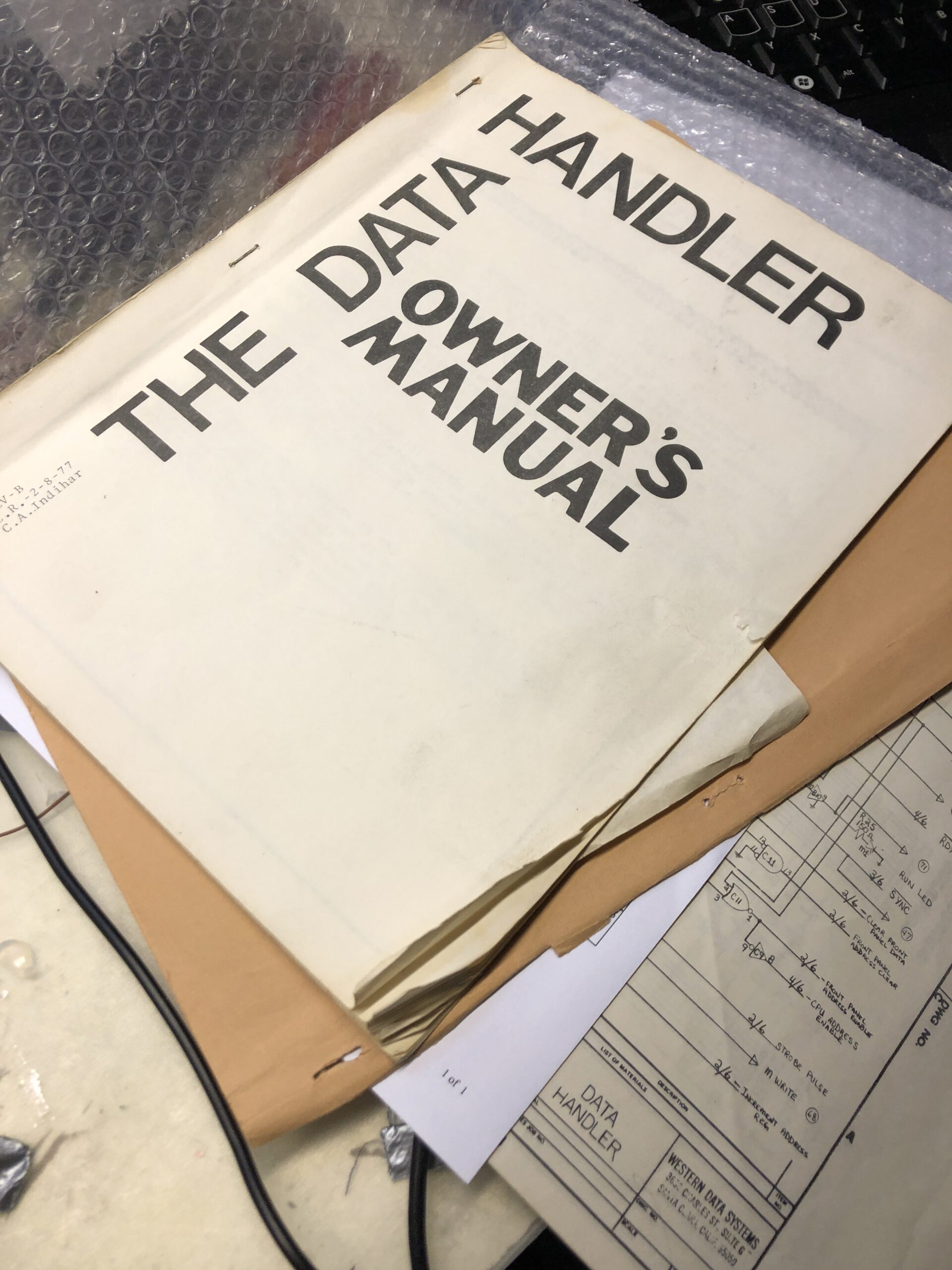
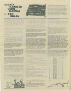
The Data Handler Owner’s Manual Rev. B |

|
The Data Handler Owner’s Manual Rev. C |
|
Data Handler Order Form |
To my current knowledge, the first „Data Handler“ Press can be found around June 1976.
The „B“ Manual shows „-2.8-77“. The „C“ Manual said „(c)1976“. While the (c)1975 indicates that it was developed and released much earlier
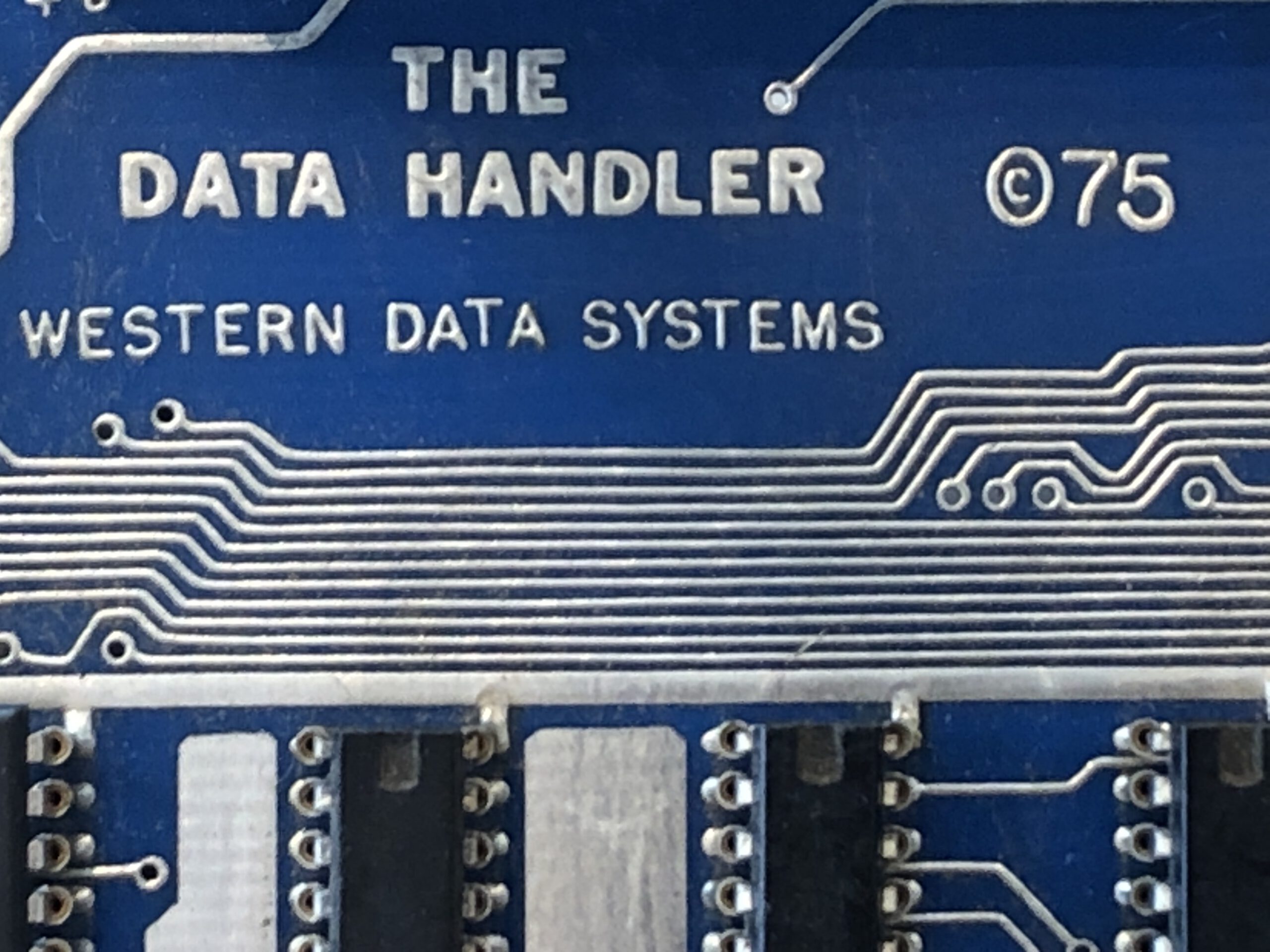
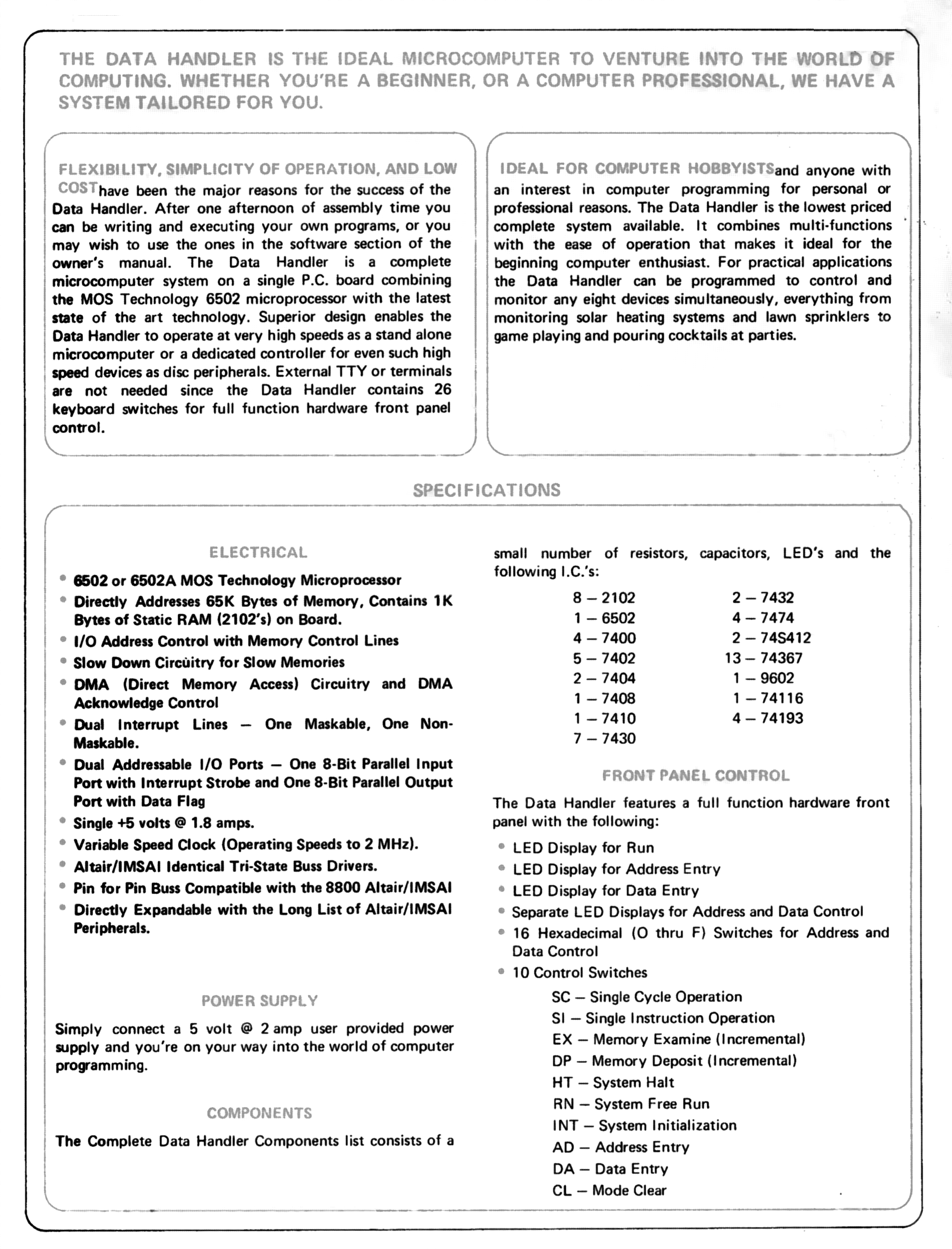
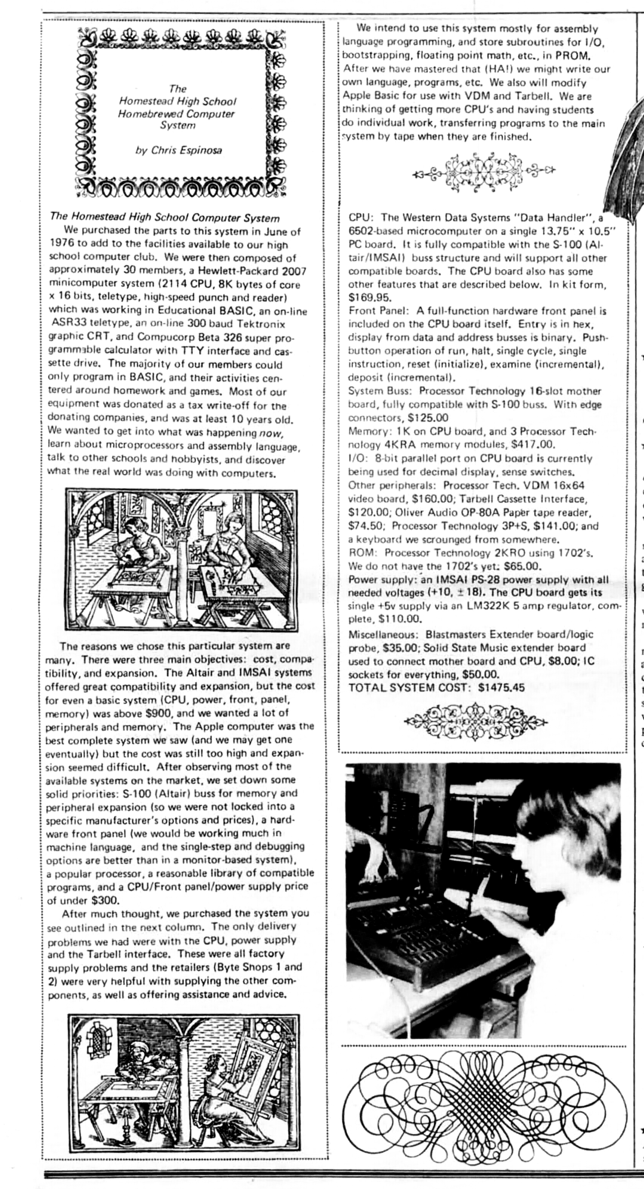
The „Data Handler“ is a Single Board Computer built in 1975 by „Western Design Systems“ Corporation. The Manual and further Literature name Mr. C.A. Indihar as the founder of Western Design Systems in Santa Clara, California .
Built around the MOS 6502 CPU, it has 1KB static RAM of Type 2102 and a „Front Panel“ with 16 Keys for Hex Entry and 10 Keys to control operation. Data „output“ is realized by 16 LEDS for Address and 8 LEDS for DATA.
- CL Clear : Clears the Adress or Data Value
- SC Single Cycle : Executes a single CPU Cycle
- SI Single Instruction : Runs one operation
- HT Halt : Stop CPU
- INT Interrupt/Reset : Start from Reset Vector
- AD Adress : Change to Modify Adress
- DA Data : Change to Modify Data
- EX Examine : Examine Data in an Address
- RN Run : CPU Run
- DP Deposit : Store Data
Data Entry into Ram is done via the Front Panel. This may be much easier than operating an MiTS or Altair, but not as comfortable as other SBC with a ROM-Monitor.
There are two I/O Ports on the upper right of the board. One Port for 8-Bit Input and one Port for 8-Bit Data output.
This is the Data Handlers Block Diagram from the REV „C“ Manual. In comparison to the „B“ Version it has an additional Cassette Interface Option. On the RAM Memory there are S-T-R Pins, which are used to split the Memory in 4 Pages.
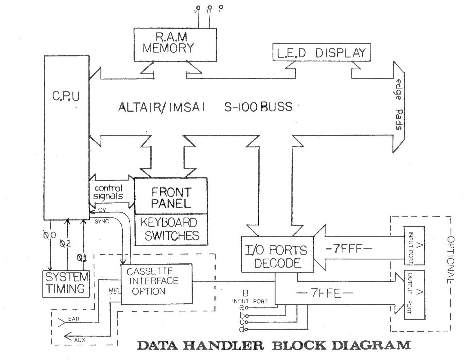
The board has a Altair compatible BUS Connector, allowing to use one of the many Expansion Cards available for Altair Systems.
Three unpopulated spare sockets are provided for system modification.
To increase system stability, the RC oscillator can be replaced by a Crystal. The SBC needs only one single 5V Supply.
An optional Regulator can be soldered on the back of the board, converting 8V power provided through the Altair Bus or an Altair Power supply to the necessary 5V.
The Manual covers the building and the operation of the Data Handler and also contains the complete Opcode description of the 6502 and the schematics of the board. In the 70s buying a manual for a chip was expensive, so having the 6502 opcodes at hand was convinient. Additionally there is also a section with a instruction lookup table.
A “program section“ contains very few simple programs to start programming.
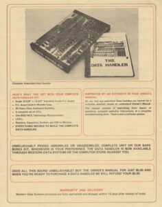
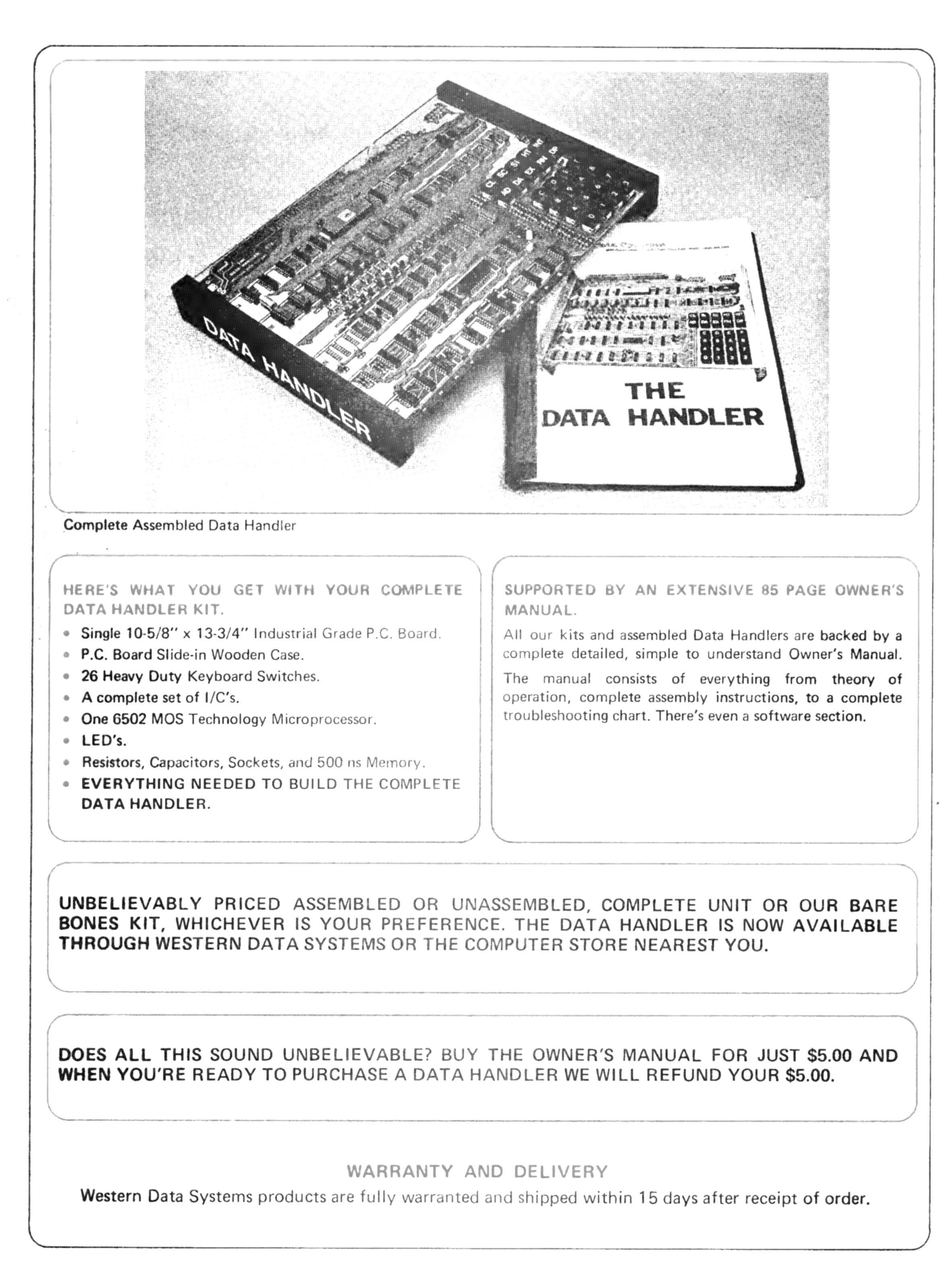
The bare board was offered for $79, the kit with all parts for $179, so it was half the price of a KIM-1.
The „Data Handler“ was a nice tool to be populated by hobbyists and to learn the Basics of 6502 machine language, but its operation requires some phantasy: Compared to the KIM-1 SBC the Data Handler has NO onboard ROM, PIA or TIA and no Monitor Program.
The „Front Panel“ is a hard wired system to enter data into Ram and start/stop and reset the CPU.
At first the CPU is Reset, then halted, and all inputs have to be cleared.
Then the program is entered in the static RAM locations. If the computation requires input data, these values have to be written in specified memory addresses. Finally you specify the start address of the program in reset vector address $FFFC and $FFFD.
The program execution is started by resetting the CPU. Manual stepping through the instructions allows to verify that the CPU jumps to program start address and runs the program.
If the calculation is finished, the CPU has to be manually halted by pressing „HT“. If there has been results of a computation, these could be viewed by examination of the corresponding memory locations.
In the rear right the we can find the I/O-Section of the SBC. It holds a strobed 8-Bit output and 8-Bit input port. Bytes written at Address 0x7FFE appear at the output port, and input data could be read from 0x7FFF. If attached some LEDS, as instructed in the Manual output could be directly controlled.
Interesting detail: output not necessarily need to be generated by program control , Data entered via the front panel could be stored at 0x7FFE directly and the result could be instantly controlled, giving a very direct response of the system.
The Board is made of 47 TTL Chips plus 8x 1kx1 RAM.
The onboard Ram is located at 0xFC00 and not 0x0000 . To my knowledge (Armin) this disables the use of any Zero Page features like POP/PUSH and indirect Addressing of the CPU. In the manual it is suggested to map RAM expansions to Address 0x0000 to enable all CPU features like Stack.
Since Address decode is done via some Gates, it seems pretty simple to modify the Address Decoder to additionally Map the existing Ram to Adresse $000x and $001x to add these features.
Operation
At first the CPU is Reset and the SI Button should be pressed four times to execute the Reset Sequence.
The program is entered in the static RAM locations. If the computation requires input data, these values have to be written in memory addresses. Additionally the start address of the program has to be stored in reset vector address $FFFC and $FFFD.
The program execution is then started by resetting the CPU. To debug the program, simply press SI-Button to follow the code. The Adress and Data LEDs show the current Program-Step. Additionally you can Cycle through an instruction with the SC-Button, follwing the CPU While fetching or storing Data from or to RAM.
By pressing the (run) RN-Button, the program executes ad maximum speed and preferrably it terminates in an endless loop.
When the calculation is finished, the CPU has to be manually halted by pressing „HT“. If there has been results, these could be viewed by pressing EX-Button and EXamination of the corresponding memory locations.
A FIRST EXAMPLE
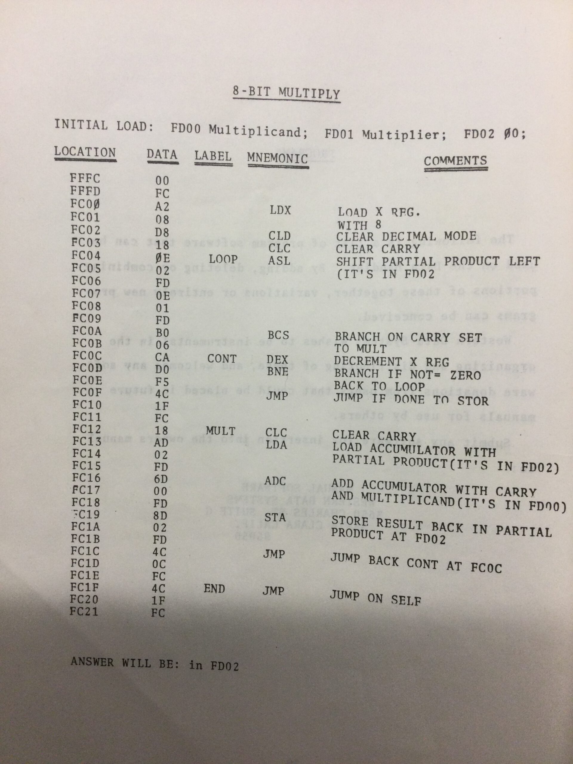
Armin tried the 8 Bit Multipy Example from the „Programmes“ Section of the Manual
To Enter the Program, I Pressed HT, CL, AD 0xFFFC, DA 0x00, and DP. So the First Byte of the Reset Vector is entered. The second byte only requires entering 0xFC and DP-Button.
To change the Adress simply Type AD 0xFC00, then DA-Button 0xA2 DP-Button to enter the first Program Byte. Next Byte is 0x08 which is entered via DP-Button. Adress increases automatically after DP-Button is pressed. During the programming process i it is possible to check the entered values via the LEDs. I was astonished how fast i get used to the simple binary display! If you misstyped the DATA, simply reenter, before pressing DP-Button. If i was not sure if the data was entered correctly, i simply retype the adress and start over a bit earlier. After i finished the program we have to deposit the two values required by the test program „Multiplicand“ and „Multiplier“ in 0xFD00 and 0xFD01. Simply Type AD 0xFD00, AD 0x02, and DP. In my test i used 0x02 for Multiplier and Multiplicand 0xFD01. This simply represents Multiply 2 by 2, and we expect 4 as a result. To verify the entered data, I used the sequence HT-SI-EX-AD 0xFD00.
To start the CPU, I pressed INT, and single-stepped through it with the single Instruction SI-Key. After some cycles the programm halted in the endless loop in 0xFC1F. By pressing HT EX 0xFD02 I could examine the result: The data LEDs „Display“ showed 0x04 ! Yippie. First Program Run Completed..!
EXPANSION
In the rear right the we can find the I/O-Section of the SBC. It holds a strobed 8-Bit output and 8-Bit input port. Bytes written at Address 0x7FFE appear at the output port, and input data could be read from 0x7FFF. If attached some LEDS, as instructed in the Manual, output could be directly controlled.
Interesting Detail: Output not necessarily need to be generated by program control: Data entered via the front panel could be stored at 0x7FFE and the result could be instantly controlled at the PIA Port without CPU Control, giving a very direct system response.
The Board is made of #47 TTL Chips plus 8x1k-RAM. The onboard Ram is located at 0xFC00 not 0x0000 to allow modification of the RESET and Interrupt Vectors.
To my knowledge this disables the use of Zero Page features like Stack (POP/PUSH), Subroutines JSR/RET, Complete Zero Page Storage and all indirect Addressing of the CPU. Only to set the Reset Vectors in Ram…Strange.
In the manual it is strongly suggested to map RAM expansions to Address 0x0000 to enable all CPU features.
Work-Around: Since Address decode is done via some Gates, it seems pretty simple to modify the Address Decoder to additionally Map the existing Ram to Adresse $00xx and $01xx to add Stack and Zero Page features.
Update August 2022: In the REV C Manual, the Manufacturer describes a Modification of the Board, which separates the 1k Memory in 4 Pages. A Jumper R,S,T, is installed which allows to Map parts of the Memory to Page 0x00,0x01 and 0xFE and 0xFF. So the System can use the Zero Page Features of the CPU.
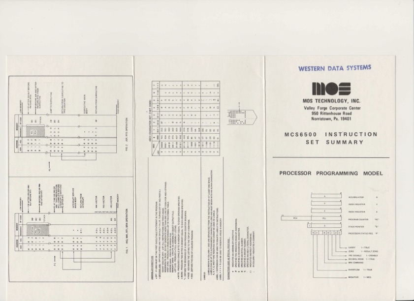
Original MOS CPU Card
The unit came with an original MOS 6500 CPU Instruction Set Summary Card, attached is a WDS Stamp.


People’s Computers 1976
 |
Articles in People’s Computers about the Data Handler |
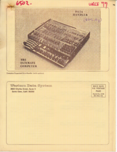 |
Original advertisement Data Handler |