The following article is a local copy of the site of Michael Cvetanovski, all design and ‘me’ in the text below is by and (C) Michael Cvetanovski.
The copy here is for information and archiving only, the original is the place to go for the latest information. The following text (“I”) is by Michael Cvetanovski.
If you are interested in the PCB’s ask Michael, not me! I do not sell them!
SYM-1 6502 mini SBC
SYM-1 Maxi
SYM-1 Maxi built by Norbert Joppen
SYM-1 6502 mini SBC
Bit of History
Once upon a time .. I had a SYM-1 sbc board that I played around with. Wonderful microcomputer for its era (early 1980’s). Like most people due to non use and lack of interest I give that micro away. Since my recent eagerness to dabble with some of the older micros .. I had a go at trying to rebuild the SYM-1 to a reasonable design so I can use most of the SYM-1 features. Having a 6502 chip and a 6532 peripheral chip, I had most bits to be able to create a minimal system to say run the SYM-1 Supermon 1.1 monitor. Following is a prototype that I got working (must admit after some testing time) which is minimal in design in having basically 5 main chips and TTL-USB adapter for comms to a PC. This project is ongoing where I have also reproduced (to a reasonable degree) an imitation keypad similar to the original one from individual pcb type push button keys. Where possible I used particular IC’s (like GAL’s) to minimise the construction and size of the design.
 Prototype Board
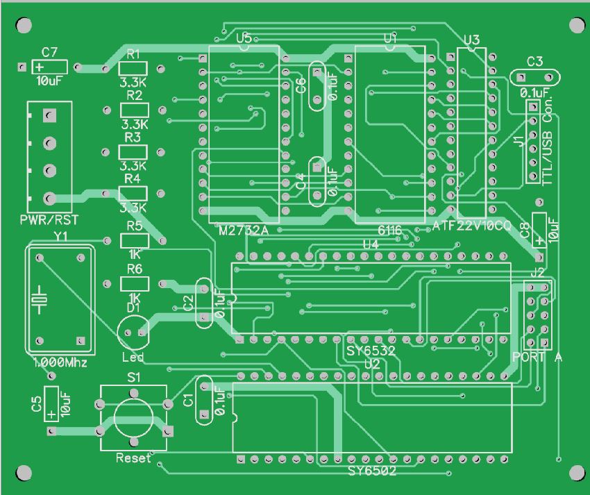
It mainly consist of the 6502 chip, 6532 peripheral chip, 2732 EPROM for Monitor, 2K 6116 Ram chip and 24pin Atmel GAL chip to provide some of the decoding and interfacing. Additional things on the board are 14pin 1Mhz crystal and an expansion socket to be able to interface to display/keypad. Flying wires are leads to a TTL to USB converter that connects to USB port of a PC. Monitor code is original version 1.1 that you can get from 6502.org. Memory map is original as per SYM-1 board for the monitor, 6532 chip and 2k RAM from 0000-07FF. Gal chip used is Atmel ATF22V10CQ/CQZ. No particular reason for this one .. but you can easily get them from RS components and not that expensive. I will provide the .pld and .jed file for the code to program these. See notes later on.
Prototype board was constructed using a vero type board with a bank of tracks to place the IC’s. Wiring was soldered point to point using wire wrap wire. After initial mounting of the components and testing for shorts etc the board was ready for use. When powered up the board draws about 220mA. See pic below.
 Parts for construction
If you are an old micro buff you probably have some if not most parts to construct this mini board. In case you don’t here is few suggestions for major parts.
- 6502, 6532 you might be lucky enough to get them from China supplies (via Alibaba or Ebay website)..be prepared to wait 3-4 weeks at least.
- Atmel pdl (GAL chip) try RS components.. usually very quick delivery. If you cannot program pld’s I can supply the chip programmed.
- 1Mhz crystal try element14
- 2732 and 6116 try www.futurlec.com. If you cannot program the 2732 I can supply some Eproms as I have some spares left.
- TTL to USB adaptor, Many supplies from China via Ebay ..take 3-4 weeks
- Also look through some forums like this one.
 Circuit Design
It basically follows from the original SYM-1 schematics, with simplification of decoding logic with a PLD chip. For minimal system you would need at least a Monitor program, some RAM and an I/O comms. Simplest would be to have RS232 type comms that you can connect to a PC and communicate to the board via terminal type program. So in that case from original design, 6532 chip did the job of communication via pins 16 and 19 to RS232 type interface. Since I was trying to use TTL to USB interface I did not have much success in interfacing the board to the PC. It wasn’t till I actually built an additional keypad to connect to the main board and played around with that I figured out the interface and comms settings. The final comms configuration involved using inverter gates for input and output to serial port (via PLD chip), and the following serial settings on comms port:
- 4800 Baud
- no parity
- 8 bit
- 1 stop bit
- handshake none
Original notes and references to RS232 on SYM-1 refer to 3 stop bits .. which confused me initially .. hence it took a while to figure out what works properly.
Schematic and component functions
Following is a schematic of the design. It is using Diptrace software. Note I use point to point schematic (pin ID connections). It does reduce wires ..but for some people it gets bit harder to follow.
Caution: As with any circuit diagrams it is up to you to recheck and make sure it is OK before proceeding to any construction. To best of my ability this is representation of what I have used. I’ve followed other circuit diagrams on the web, only to find some info was wrong. So please check pin outs (especially against datasheets) to make sure all connections are correct. If there is any errors please email me.
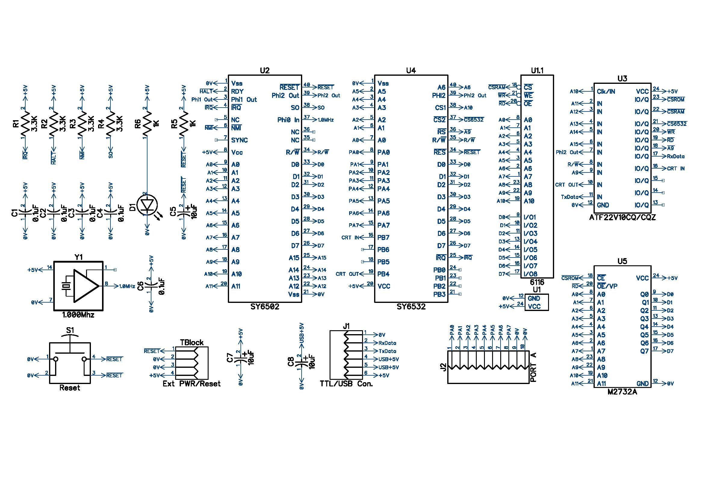
Looking at the schematic here is bit of explanation of some of the component functions:
- Resistors are basically pullup resistors for inputs to CPU that are not needed.
- R6 and D1 are just power indicator for the board.
- S1 (on board pb switch), C5 and R5 are the reset input to 6502. Note also reset is provided from external input via terminal power block.
- 6532 is wired similar to SYM-1 schematic: A0-A6 for on chip ram addressing. CS1 is A10 and Register Select (RS) is via PLD chip. R/W is direct from 6502.
- Chip selects for Rom, Ram and 6532 come from PLD.
- CRT OUT is inverted to RxData ..so is TxData to CRT IN via PLD inverter gates.
- PLD provides address decoding and 3 inverter gates. Phi2 and R/W are used to generate RD and WR signals for Rom/Ram.
- 6116 and 2732 can be any brand as long as the pins are same. Also note which programming voltage is used for the 2732 chip, as they vary greatly.
PLD Function
Atmel PLD is used to provide address decoding and 3 gate inverts for A9 and serial signals. For more info see Atmel website and WinCupl software.
The code for the PLD is shown below:
Name SYM-1;
Partno 0001;
Revision 4k Mon, 2kRam, 6532 Comm;
Date 6/2/15;
Designer mc;
Company mcoz;
Location oz;
Assembly manual;
Device g22v10;

/** Inputs **/
pin [1..6] = [a10..15] ;
pin 7 = phi2;
pin 8 = rnw;
pin 9 = a9;
pin 10 = crtout;
pin 11 = crtin;

/** Outputs **/
pin 19 = !nr;
pin 20 = !nw;
pin 21 = !cs6532;
pin 23 = !csrom;
pin 22 = !csram;
pin 18 = !na9;
pin 16 = !ncrtin;
pin 17 = !ncrtout;

/** Declarations and Intermediate Variable Definitions **/

field ioaddr= [a15..9];
cs6532_eqn = ioaddr:[A4XX..A7XX];
csrom_eqn = (ioaddr:[80XX..8FXX])#(ioaddr:[F0XX..FFXX]) ;
csram_eqn = (ioaddr:[00XX..07XX]) ;

/** Logic Equations **/

ncrtout=crtout;
ncrtin=crtin;
na9=a9;
nr =phi2&rnw ;
nw = !rnw&phi2 ;
cs6532 = cs6532_eqn ;
csrom = csrom_eqn;
csram = csram_eqn;
The pinout for PLD is as follows:

Testing the board
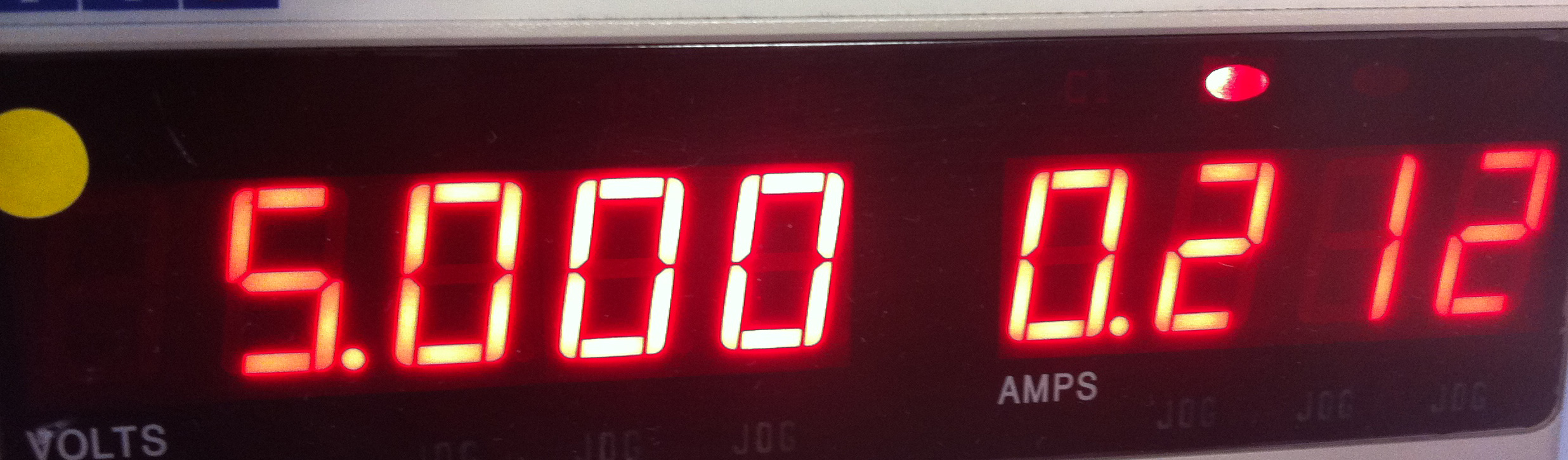
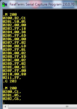
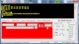
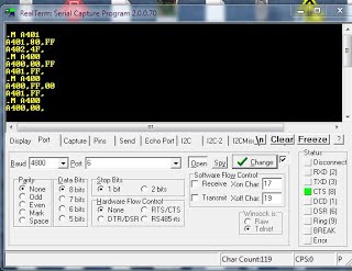
Obviously have the board connected to the PC and use appropriate comms software like Hyperterm (on XP) or RealTerm set to appropriate setting. Also set CAPS ON. (reduces errors). If all OK after pressing the RESET button …press the “Q” key on keyboard . The response should be “.” single dot …where you can give monitor commands after that. Following is snapshot of sample program that is given in Reference manual for SYM-1 that adds two numbers together from memory locations 200 and 201 and places result in 202. You can see that 202 changed from 0 to C6 which is = C1+05.
From this point on you can explore all the monitor commands. Save and Load will not work as provision is not made in this design for saving code to cassette tape. So another way of saving and loading the machine code is via SP an LP (paper tape commands).
Saving and loading code (via terminal)
Refer to paper tape format info in SYM-1 Reference manual (page D-1). So for example to save above code you would issue command
SP 200-210
and before you press , set terminal program to capture file mode.. which will save text as it is output to the terminal.
Start capture mode and press
the listing should follow.. once character output had stopped ..Stop the capture …
To see what is captured open the captured file with Notepad..it should look like something like this …
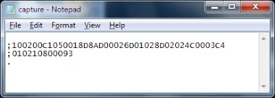
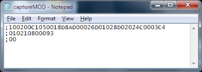
Delete the space in first line and replace the “.” in the last line with “;00”. This creates the correct file to upload.
To retrieve the code type in
LP
and send the captured file as text using terminal program ..What you might need to do is delay the character and LF output to about 20ms so the board does not get swamped with incoming characters from the PC serial port. You can adjust the delay to smaller value till the sending of file stops working properly. 20ms+ is usually a safe bet.
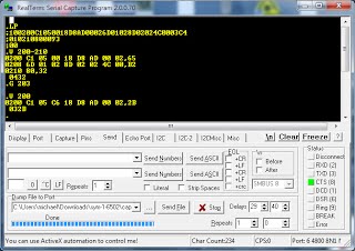
Picture above shows loading of the file, listing the code, running it and then listing the result of the addition program. So there you are ..plenty of things to be able to examine ..with minimal system similar to the original SYM-1 board.
I/O via 6532 PIA chip
Ok If you are to use the mini board with RS232 interface only (that is … with NO keypad/display) then the port A (address A400) is free to use for any I/O control. The DDRA (address A401) can be set up for output or input. As a simple example using SYM monitor we can set the DDR to output on all eight PA pins (set DDRA to FF). Then changing the value of I/O Register A (A400 address) from FF to 00 will toggle output on the port A (pins 8-15) from high back to low.
If you want to use the port A as an input then set appropriate bits to 0 in DDRA. Image below shows a crude example of control via Monitor commands. Writing machine/assembly code for more complex task is possible and make the board useful as a micro controller.
Running mini @9600 Baud
It is possible to run the mini board @ 9600. Suggestions have been obtained from 6502 pages website, where following address have been changed:
8AE9 08 --> EA         '   NOP
8AEA 48 --> 60          '  RTS

8AB0 0B -->0A           ' CHANGE NUMBER OF STOP BITS
Changed binary file Supermon 1.1 file for 9600 baud can be downloaded from here. Please note as suggested, once this is changed it might not be possible to run the board at different speeds.
PCB for mini SYM-1
If you are like me I am not best at bread boarding circuits. From the mini board schematic diagram I have generated a pcb design and gerber files that you be able to make your own boards from. See link below.
Word of Caution First
I have not made any of these pcb’s so make sure you check the board out before any component mounting. In case there is any major faults let me know. One mistake that I am aware of is that the polarized caps C5,7 and 8 show the “+” on the wrong side. So make sure you mount polarized caps the correct way around. When I get time will try to correct that.
At this point I am only providing the full set of the gerber files from which you can get the boards manufactured. From more expensive pcb websites the board will work out about $30-$40 .. but if you shop around and get more than one board ..they will probably work out $10-15 each.
Top silk layout and component placement
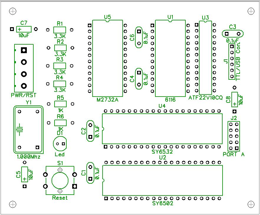
Most of component placement is self explanatory. It is possible to power the board from TTL/USB connector (by getting +5 volts from PC USB port). But word of caution in doing that. The setup draws about 220mA, so make sure all the connection on J1 are solid. Also if you to use USB power then do not power the board from PWR/RST connector.
Bottom traces…
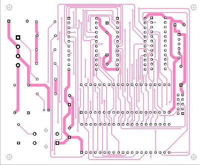
Top Traces ..
.
Download set of zipped Gerber files here.
SYM-1 Keyboard
 Following is info about keyboard and 6 digit 7 segment display expansion prototype board that was used with mini SYM board to run monitor program from the keypad. It is similar in layout to original SYM-1 board. Keys are made up of pcb push button switches, that have 2 square caps on them. One cap clips over the switch then another CLEAR plastic cap clips over the top again. By placing appropriate size bit of paper with text on it, ANY keyboard key indicator can be made up. (see picture)
The only issue with these switches is that they had too much horizontal (rotational) play and hence keys do not look all lined up. Placing the keys close would eliminate some of that, however mounting the switches on the pcb requires some distance between adjoining pins – so it is not possible to bring the rows close together.
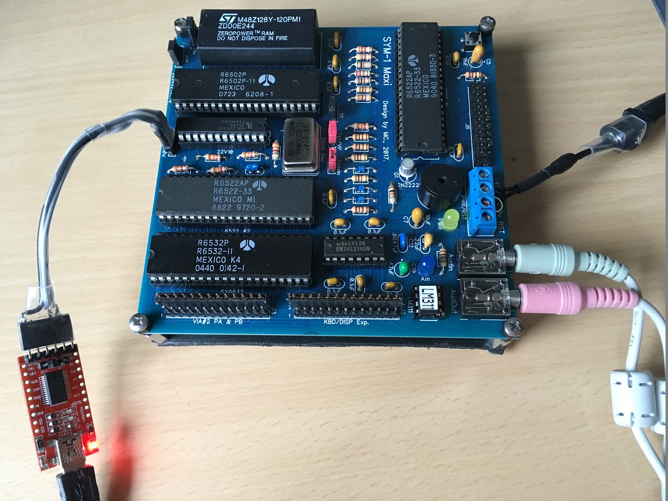
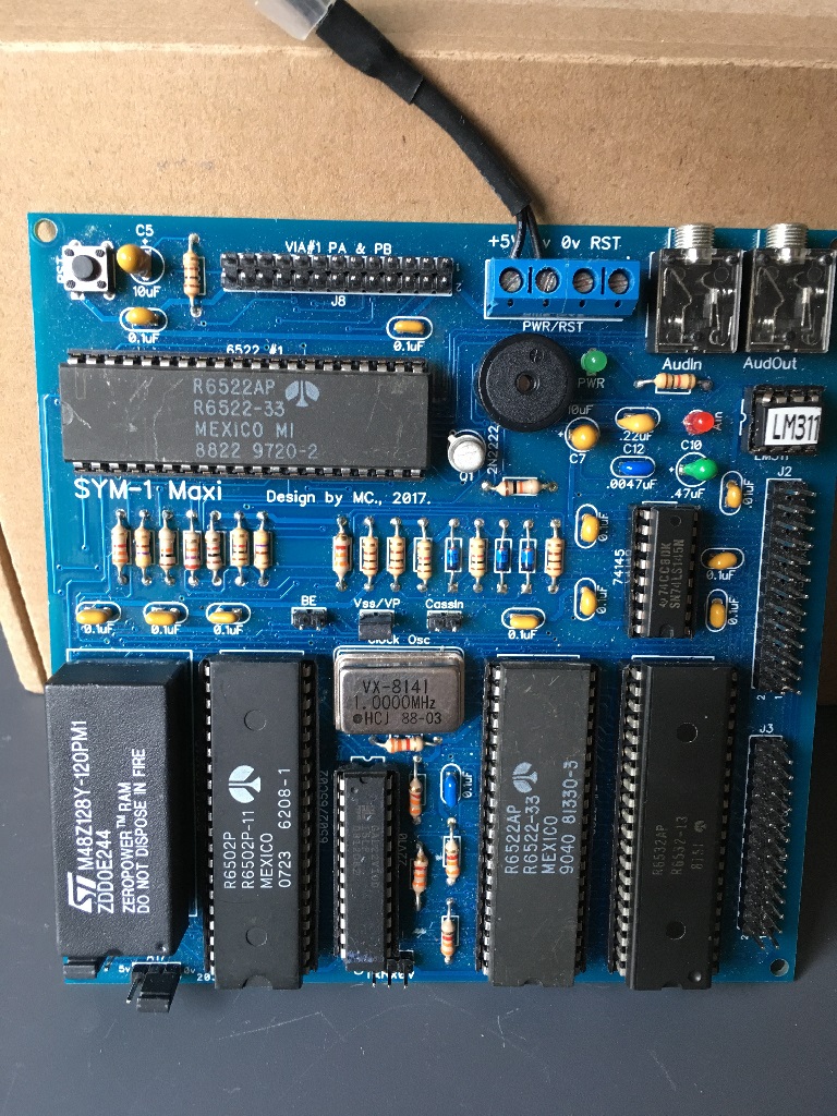
SYM-1 Maxi
This design follows on from the SYM-1 mini board.
- It improves on previous design by increasing the memory size to possibly full 64K, using NVRam as both RAM and ROM with GAL chip for decoding.
- 6532 chip is used for comms and general PIO …or possible connection to external keypad (like the original SYM-1 board).
- There is provision for 2 extra 6522 chips to give extra VIO capabilities to the board.
- It should be possible to implement the original Monitor software plus any other software like BASIC or the assembler/editor.
- Communication to the board is via TTL to USB converter and a need for terminal program like REALTerm.
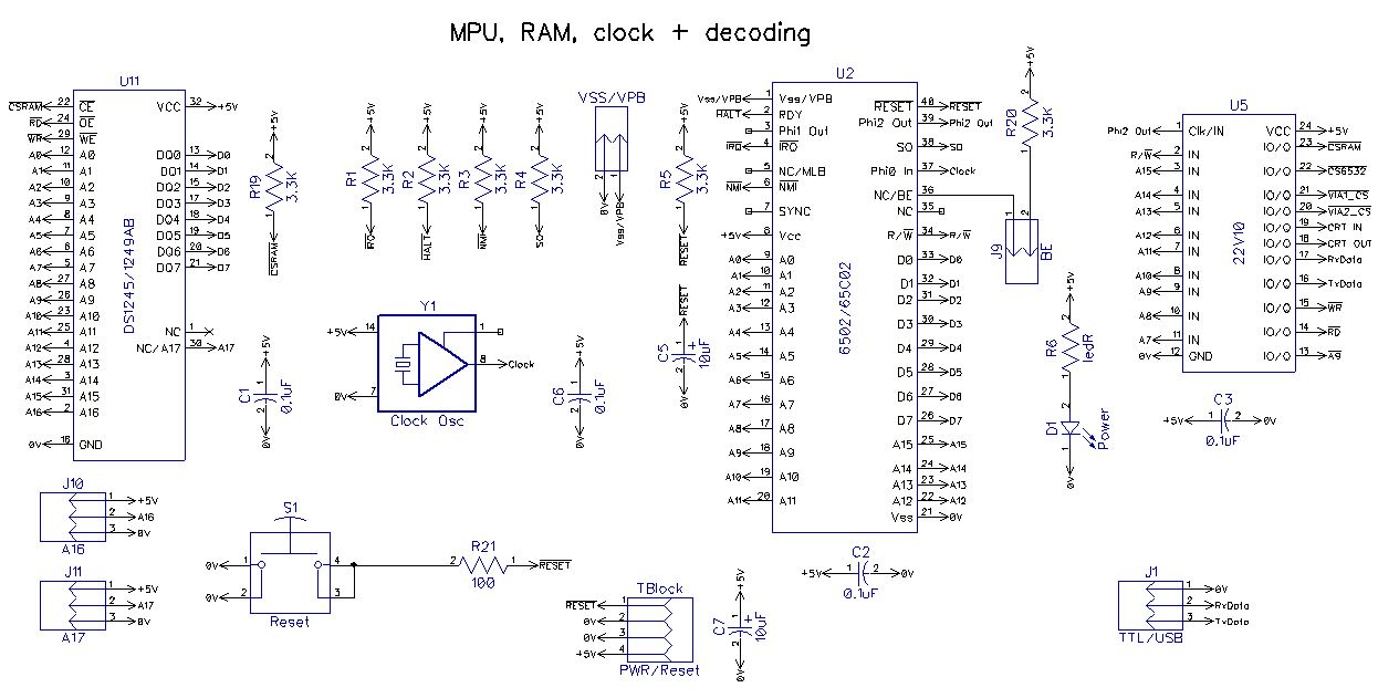
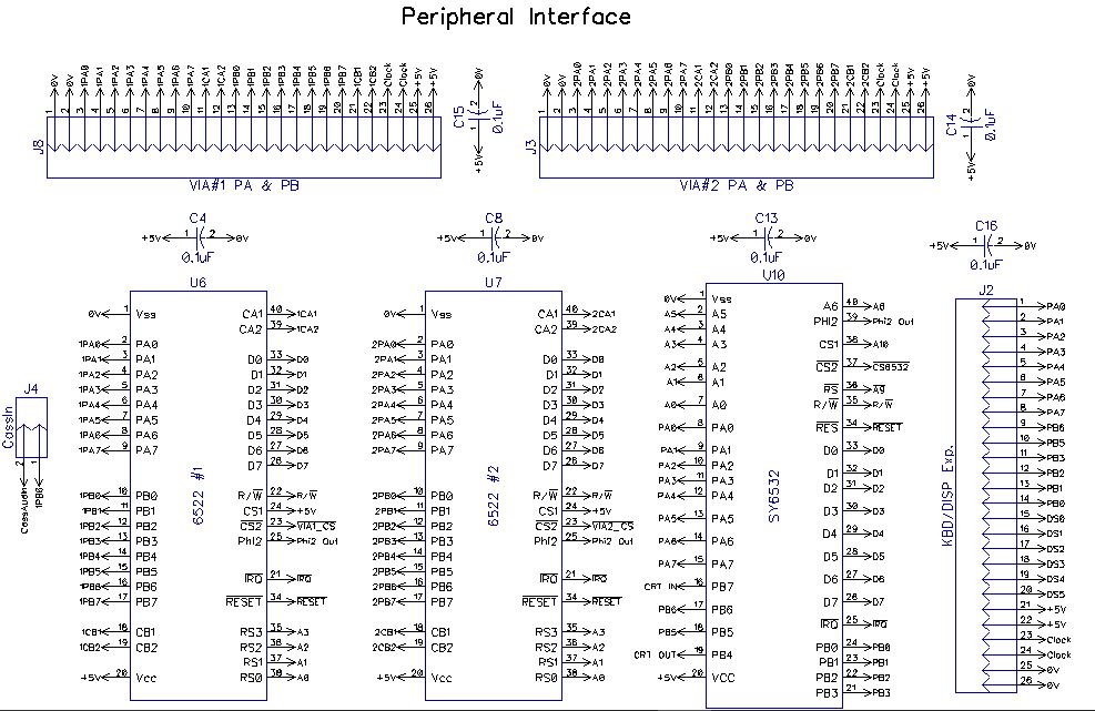
Following is the schematic of the design:

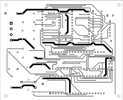
Following is a TOP view of the manufactured PCB ..
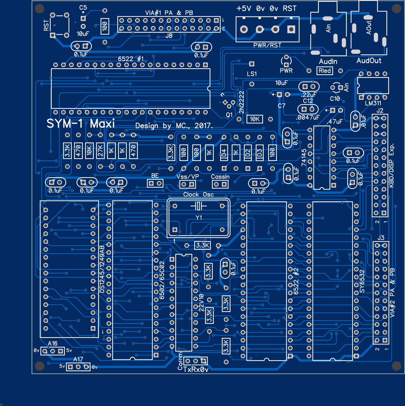
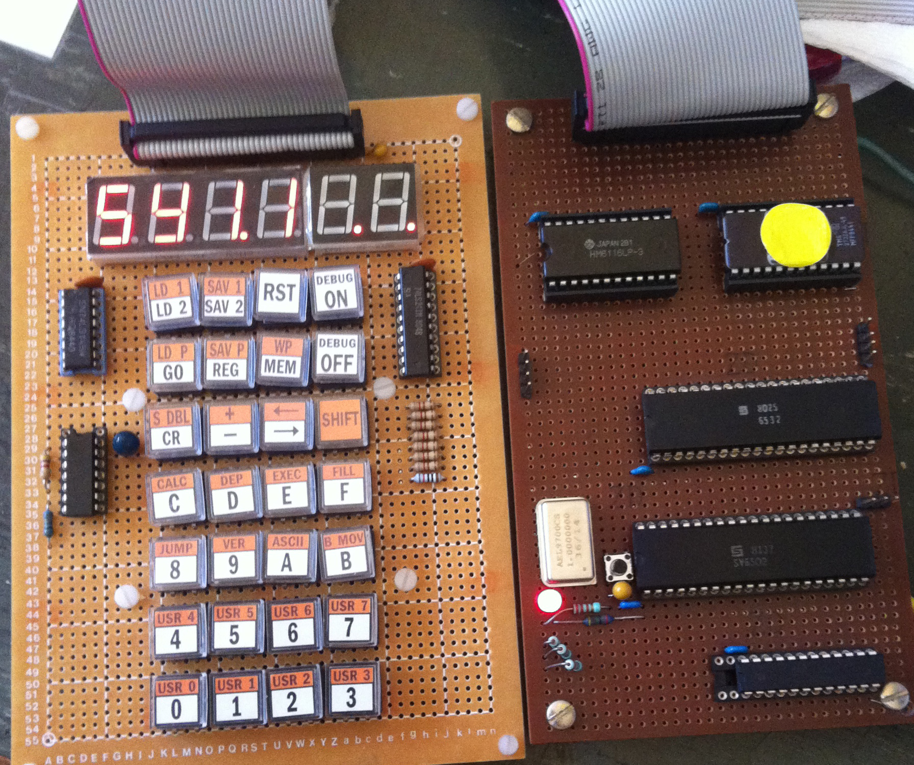
And image of assembled board (most of it tested ) …
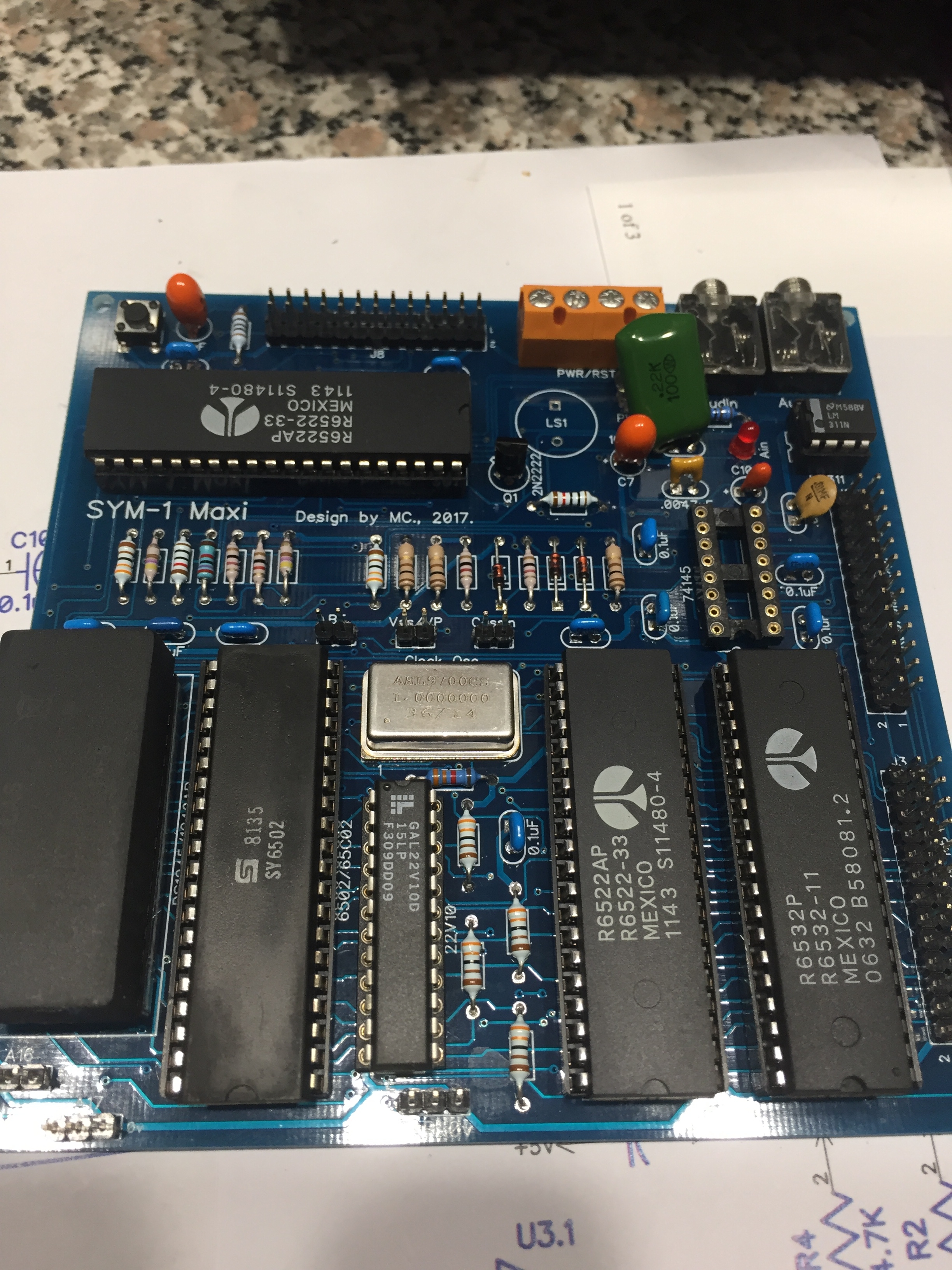
Current consumption of the board with all chips on board is about 270mA … that is without any external connections to VIA chips ..
There is a slight mod …looking at the above schematic ..pins 18 and 13 have to be swapped ..that is pin18 becomes !a9 and 13 becomes crtout… reason being the the default schematic for the gal chip had pin 13 as i/o pin … but it is only an input pin ..!!!
PLD file to make it all work ….
Name            SYM-1 Maxi;
Partno          0001;
Revision        ver4,monitor,basic,RAE ;
Date           23/11/17;
Designer        mc;
Company         mcoz;
Location        oz;
Assembly        manual;
Device          g22v10;

/** Inputs **/
pin [3..8] = [a15..10] ;
pin 1 = phi2;
pin 2 = rnw;
pin 9 = a9;
pin 10 = a8;
pin 11 = a7;
pin 13 = crtout;
pin 16 = crtin;

/** Outputs **/

pin 14 = !nr;
pin 15 = !nw;
pin 22 = !cs6532;
pin 18 = !na9;
pin 20 = !via2cs;
pin 21 = !via1cs;
pin 23 = !csram;

pin 19 = !ncrtin;
pin 17 = !ncrtout;

/** Declarations and Intermediate Variable Definitions **/

field ioaddr= [a15..7];
cs6532_eqn   = ioaddr:[A4XX..A7XX];
csrom_eqn   = (ioaddr:[80XX..8FXX])#(ioaddr:[B0XX..FFXX]) ;
csram_eqn   = (ioaddr:[00XX..7FXX]) ;

/** Logic Equations **/

ncrtout=crtout;
ncrtin=crtin;
na9=a9;
nr = phi2&rnw ;
nw  = !rnw&phi2 ;
cs6532 = cs6532_eqn ;
csrom = csrom_eqn&nr;
csram = csram_eqn#csrom;
You can source all binary files from 6502.org or try this combined file that has
Monitor imaged @8000-8FFF and F000-FFFF
Basic imaged from C000-DFFF and
RAE imaged @B000-BFFF and E000-EFFF
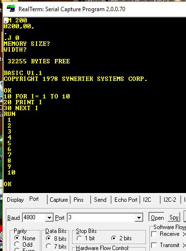
Following is a screen capture of SYM-1 Monitor and SYM BASIC running on maxi Board …
To explore the feature of saving a file to tape cassette do the following …
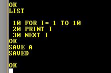
After typing in “SAVE A” and monitor the output on pin 9 of 74ls145..it should be pulsing for a while while the code is being transferred. The rest of circuitry converts the TTL pulses so they can be saved in appropriate audio signals levels for a tape input . Should be able to use any reasonably good tape recorders ..or even modern digital voice recorders ..for saving the code (basic text file) on tape. Similar procedure can be used for saving memory code from Monitor Program via S1 or S2 commands.
RAE for SYM-1
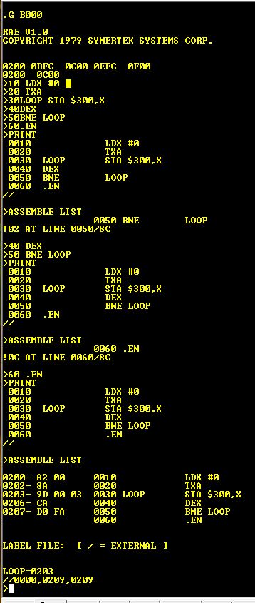
To run the RAE (Resident Assembler Editor) on maxi board ..just type in “G B000” from the monitor prompt .. see image below which shows some test editing and assembling using RAE ..Very Nice …
For more information: see the SYM-1 RAE page.
SYM-1 Maxi build by Norbert Jopppen
After some modifications to the pld file , the cassette interface, the6522’s and the 6532, Basic and RAE are working now. The problems Norbert had were oscillating circuits. Then Norbert found out that the NVRAM is quite critical. On his board a M48Z128Y-120PM1 works well. The Dallas DS1245AB was not reliable.
PLD files by Norbert for the SYM-1 Maxi