Bug in the TTY KIM-1 monitor

The KIM-1 monitor surprises me every time I dive into it.
The KIM-1 Explained is nearing completion. The KIM-1 explained

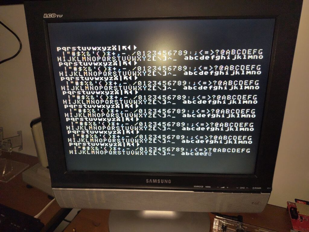
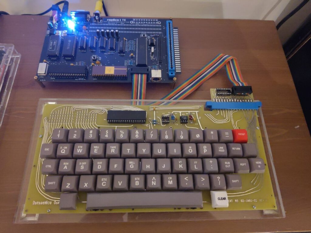
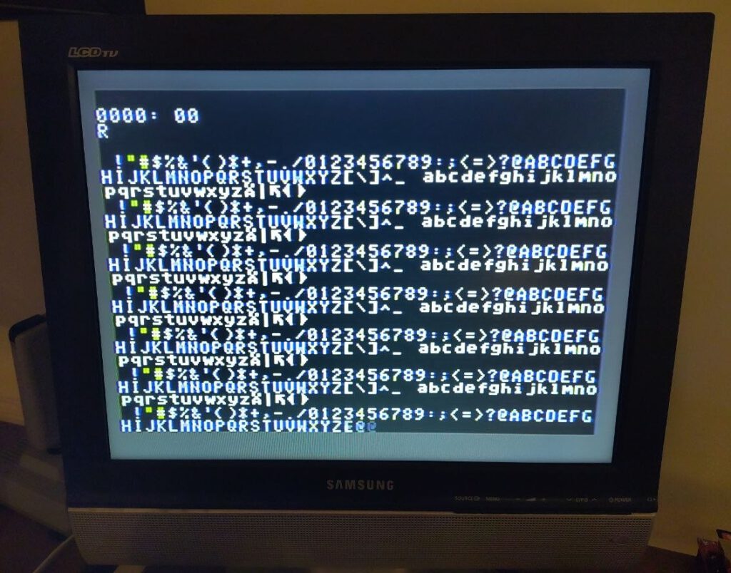
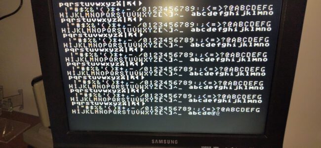
There is a bug in the TTY CLI, it accepts characters as ‘;’ and ‘:’ as valid hex and translates to A..F.

KIM
0200 A9 ;;
00BB 00 ::
00AA 00 ????
FFFF 1C

More about this innocent feature here: PRTBYT, GETBYT and PACK

PRTBYT, GETBYT and PACK

PRTBYT takes a byte and sends it to the serial TY as two hex ascii characters
The byte is entered in A, two characters are printed and A is saved.

0914   1E3B             ;		
0915   1E3B             ;       PRINT 1 HEX BYTE AS 2 ASCII CHAR'S
0916   1E3B             ;   
0917   1E3B 85 FC       PRTBYT  STA   TEMP                             
0918   1E3D 4A                  LSR   A           ; SHIFT CHAR RIGHT 4 BITS
0919   1E3E 4A                  LSR   A
0920   1E3F 4A                  LSR   A
0921   1E40 4A                  LSR   A
0922   1E41 20 4C 1E            JSR   HEXTA       ; CONVERT TO HEX AND PRINT
0923   1E44 A5 FC               LDA   TEMP        ; GET OTHER HALF
0924   1E46 20 4C 1E            JSR   HEXTA       ; CONVERT TO HEX AND PRINT
0925   1E49 A5 FC               LDA   TEMP        ; RESTORE BYTE IN A AND RETURN
0926   1E4B 60                  RTS   
0927   1E4C             ;
0928   1E4C 29 0F       HEXTA   AND   #$0F        ; MASK HI 4 BITS
0929   1E4E C9 0A               CMP   #$0A
0930   1E50 18                  CLC   
0931   1E51 30 02               BMI   HEXTA1
0932   1E53 69 07               ADC   #$07        ; ALPHA HEX
0933   1E55 69 30       HEXTA1  ADC   #$30        ; DEC HEX
0934   1E57 4C A0 1E            JMP   OUTCH       ; PRINT CHAR

What is happening here?

  • The byte in A is saved (917)
  • the high nibble is shifted to the lower nibble (918-921)
  • the nibble is converted to hex (922, calls hexta)
  • the byte is restored and the low nibble converted to hex
  • A is restored
    • hexta masks off low nibble (928)
    • convert A..F to ascii (929-932)
    • convert hex to ascii and print(933-934)

    GETBYT and PACK

    1148   1F9D             ;		
    1149   1F9D             ;       GET 2 HEX CHAR'S AND PACK 
    1150   1F9D             ;       INTO INL AND INH
    1151   1F9D             ;       X PRESERVED Y RETURNED = 0
    1152   1F9D             ;       NON-HEX WILL BE LOADED AS NEAREST HEX EQU
    1153   1F9D             ;
    1154   1F9D 20 5A 1E    GETBYT  JSR   GETCH
    1155   1FA0 20 AC 1F            JSR   PACK
    1156   1FA3 20 5A 1E            JSR   GETCH
    1157   1FA6 20 AC 1F            JSR   PACK
    1158   1FA9 A5 F8               LDA   INL
    1159   1FAB 60                  RTS
    1160   1FAC             ;		
    1161   1FAC             ;       SHIFT CHAR IN A INTO
    1162   1FAC             ;       INL AND INH 
    1163   1FAC             ;
    1164   1FAC C9 30       PACK    CMP   #$30       ; CHECK FOR HEX 
    1165   1FAE 30 1B               BMI   UPDAT2
    1166   1FB0 C9 47               CMP   #$47       ; NOT HEX EXIT
    1167   1FB2 10 17               BPL   UPDAT2
    1168   1FB4 C9 40               CMP   #$40       ; CONVERT TO HEX
    1169   1FB6 30 03               BMI   UPDATE
    1170   1FB8 18                  CLC   
    1171   1FB9 69 09               ADC   #$09
    1172   1FBB 2A          UPDATE  ROL   A
    1173   1FBC 2A                  ROL   A
    1174   1FBD 2A                  ROL   A
    1175   1FBE 2A                  ROL   A
    1176   1FBF A0 04               LDY   #$04       ; SHIFT INTO I/O BUFFER
    1177   1FC1 2A          UPDAT1  ROL   A
    1178   1FC2 26 F8               ROL   INL
    1179   1FC4 26 F9               ROL   INH
    1180   1FC6 88                  DEY   
    1181   1FC7 D0 F8               BNE   UPDAT1
    1182   1FC9 A9 00               LDA   #$00       ; A=0 IF HEX NUM
    1183   1FCB 60          UPDAT2  RTS
    

    What is happening here?

    GETBYT
    The GETBYT routine is used in the TTY part of the KIM-1 monitor to enter two hex characters (0..9 and A..F) and pack it into one byte.

    • read the first character (1154)
    • pack it into INL lower nibble (1155)
    • read the second character (1156)
    • pack it into INL, shifting the lower nibble to high and shifting in the second nibble (1157)
    • return byte from INL to A

    PACK

    • check if < '0' and error out with A > 0 (1164-1165)
    • check if > ‘F’ and error out with A > 0 (1166-1167)
    • if A..F add $09 (1168-1171)
    • shift in nibble via INH and INL
    • return zero if valid hex but with invalid Z flag

    Note that the range between ‘9’ and ‘A’ is not checked, so those are taken as valid hex characters.
    The PACK routine accepts ‘:’– ‘?’, $3A .. $3F as valid hex characters A ..F.

    KIM
    0200 A9 ;;
    00BB 00 ::
    00AA 00 ????
    FFFF 1C
    

    The ASCII encoding is arranged so that adding 9 to ‘A’–’F’ aligns them perfectly with the desired hexadecimal nibble after four left rotates. This avoids a separate subtraction of ‘A’ and addition of 10.

    The following demo with PRTBYT and GETBYT illustrates how this could be done in a user program.

    0001   0000             ;
    0002   0000             ; GETBYTC with error checking
    0003   0000             ; illustrates shortcomings in PACK
    0004   0000             ; - G and ; and possibly more accepted without error
    0005   0000             ;
    0006   0000             ; Demo of program: 
    0007   0000             ; KIM
    0008   0000             ; 0000 00 200
    0009   0000             ; 0200 A9 G
    0010   0000             ; &gt;12=12
    0011   0000             ; &gt;33=33
    0012   0000             ; &gt;G?
    0013   0000             ; &gt;H?
    0014   0000             ; &gt;GG=00
    0015   0000             ; &gt;;;=BB
    0016   0000             ; &gt;AB=AB
    0017   0000             ; &gt;CD=CD
    0018   0000             ; &gt;EE=EE
    0019   0000             ; &gt;
    0020   0000             ;
    0021   0000             ; KIM-1 defines
    0022   0000             ;
    0023   0000             PACK 	= 	$1FAC		; pack hex character into INL, shift in
    0024   0000             PRTBYT	= 	$1E3B		; print byte as 2 hex characters
    0025   0000             GETCH	=	$1E5A		; receive character from TTY serial
    0026   0000             OUTCH	= 	$1EA0		; send character via TTY serial
    0027   0000             INL		= 	$F8	
    0028   0000             INH		= 	$F9
    0029   0000             ;
    0030   0200             	.org $0200
    0031   0200             
    0032   0200             ; demo code
    0033   0200             ;
    0034   0200 A9 00       LOOP 	LDA	#$00
    0035   0202 85 F8       		STA INL			; zero hex byte
    0036   0204 85 F9       		STA	INH
    0037   0206 20 3E 02    		JSR CRLF
    0038   0209 A9 3E       		LDA #&#039;&gt;&#039;		; prompt
    0039   020B 20 A0 1E    		JSR OUTCH
    0040   020E 20 28 02    		JSR GETBYTC
    0041   0211 90 08       		BCC OK
    0042   0213 A9 3F       		LDA #&#039;?&#039;		; error
    0043   0215 20 A0 1E    		JSR OUTCH
    0044   0218 4C 00 02    		JMP LOOP
    0045   021B             ;		
    0046   021B 48          OK		PHA
    0047   021C A9 3D       		LDA	#&#039;=&#039;
    0048   021E 20 A0 1E    		JSR OUTCH
    0049   0221 68          		PLA
    0050   0222 20 3B 1E    		JSR PRTBYT
    0051   0225 4C 00 02    		JMP LOOP		; repeat	
    0052   0228             ;
    0053   0228             ; subroutine GETBYTC
    0054   0228             ; read 2 hex characters from TTY input
    0055   0228             ; pack into one byte
    0056   0228             ; Returns: carry clear if hex OK, A == hex byte
    0057   0228             ; clobbers X and Y
    0058   0228             ;
    0059   0228             
    0060   0228             
    0061   0228 20 5A 1E    GETBYTC	JSR	GETCH		; read character
    0062   022B 20 AC 1F    		JSR	PACK		; pack into INL
    0063   022E D0 0C       		BNE     EGETB		; A = 0 if hex number
    0064   0230 20 5A 1E    		JSR	GETCH		; read second character
    0065   0233 20 AC 1F    		JSR	PACK		; pack into INL
    0066   0236 D0 04       		BNE     EGETB		; A = 0 if hex number
    0067   0238 A5 F8       		LDA	INL
    0068   023A 18          		CLC
    0069   023B 60          		RTS
    0070   023C 38          EGETB	        SEC
    0071   023D 60          		RTS
    0072   023E             		
    0073   023E A9 0D       CRLF	        LDA 	#$0D
    0074   0240 20 A0 1E    		JSR 	OUTCH
    0075   0243 A9 0A       		LDA 	#$0A
    0076   0245 20 A0 1E    		JSR		OUTCH 
    0077   0248 60          		RTS
    0078   0249             
    0079   0249             		.END
    0080   0249             		
    0081   0249             
    tasm: Number of errors = 0
    

Programming tips

Some tips that I learned programming for the KIM-1 and the 6502.

ALWAYS CHECK YOU DO NOT FORGET IMMEDIATE ACCESS SYNTAX!
It so easy an common to forget the ‘#’ in your assembler code. Assemblers will not complain and make it absolute or zeropage addressing and you will search for hours!

TTY routines

Do not use the CRLF routine at $1E2F in the monitor

This routine sends the CR and LF to the TTY output vai OUTCH. Nice, you will need that often in a console program.
But if you read the page on printing a string you see this routine also sends out 6 Null ($00) characters, this takes a lot of wasted time!

Just make your own subroutine

LDA #$0D   ; CR
JSR OUTCH
LDA #$0A   ; LF
JSR OUTCH
RTS

Note that this destroys A and Y!

GETCH gets a character to serial TTY.
Blocking, it waits indefinitely for a character to arrive and A will have the value.
The routine also kills the Y register, returns with Y = $FF.
Also, in LED Display and Keyboard mode, it returns with A = $01 and X = 8.
Save Y before calling GETCH, and restore Y when it returns.

OUTCH sends a character to serial TTY
No handshaking, no hardware flow control, it just spits out the character.
A destroyed, Y=FF, X preserved.
Save at least Y, and saving A is recommended.

SPACE print a blank

This just calls OUTCH with A = $20, so read OUTCH for the side effects.

PRTBYT Print A as two hex characters

Uses OUTCH, so Y is lost. A is preserved.

GETBYT and GETBYTC

X saved, Y = 0, A is hex character
Reads two hex characters (0..9 A..F) and tries to pack them in A.
See the page on PRTBYT,GETBYT and PACK for an error checking alternative GETBYTC to GETBYT.
Note that due to an incomplete check ‘:’– ‘?’, $3A .. $3F are accepted as valid hex characters A ..F.

KIM
0200 A9 ;;
00BB 00 ::
00AA 00 ????
FFFF 1C

The audio tape routines

The DUMPT and LOADT routines are OK to call interactively to dump and load KIM-1 files on tape.
The cannot be called as subroutines. when finished they return to the KIM-1 monitor.
DUMPT return with $0000 as current address pointer in the KIM-1 monitor.
LOADT returns it status via the current address pointer in the KIM-1 monitor, $0000 is success, $FFFF is a loading error.

What you can do is:
– Have code at $0000 to return to your program (Warm start entry), so the user just has to press G
– instruct the user what to do if DUMPT returns $FFFF

The better solution is to incorporate Hypertape as callable subroutine.

Return to the KIM-1 monitor

The preferred location to call to enter the KIM-1 monitor form a user program is START at $1C4F

Reading the keyboard and lighting the display

Fill F9, FA, FB with the values to show on the LED displays
Call SCAND
Call SCAND to debounce
CaLl GETKEY
Now check the key in A:
– above $14 : no key
– 14 = PC
– 13 = GO
– 12 = +
– 11 = DA
– 10 = AD
– 0 ..9 A – F keys
Handle key and loop back to the begin

Serial interface with RTS CTS handshake

To use a HEathkit H14 matrix printer in 1980 I have written a serial send character routine, inspired by OUTCH on Port B pin 0.
The first version was simple, like OUTCH, at low speed to let the printer have time to do its work.
The second version added RTS/CTS handshaking via a second Port B pin as input.
Both were published in the Dutch KIM Club magazine in 1980 and 1981, together with a parallel keyboard routine and integration into the MICO ADE Editor/Assembler.

Here I present the drivers, in a more general format to have a second serial output on the KIM-1 optionally with handshake.

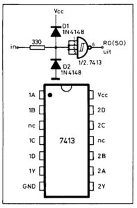
The hardware to adapt the KIM-1 to the RS232C levels can be kept simple. Here some examples:

You can find the sources in TASM32 format here.


0001   0000             ;
0002   0000             ; Serial output for example to drive a printer connected to a KIM-1
0003   0000             ; 1980 Original by Hans Otten
0004   0000             ; 2026 Cleaned of MICRO ADE artefacts and converted to TASM 
0005   0000             ;
0006   0000             ; Original in MICRO ADE syntax, curent version TASM32 Hans Otten, 2026
0007   0000             ;
0008   0000             ; Serial output routine (inspired by OUTCH in KIM-1 monitor) 
0009   0000             ; 
0010   0000             ; Send a byte in RS232C format via a PIA bit
0011   0000             ; 
0012   0000             ; Choose MASK0 and MASK1 so any pin of a PIA can be ued
0013   0000             ; Choose OUT for any PIA 6520/6521/6522/6530/6820/21. A 6522 VIA needs other initialization
0014   0000             ;
0015   0000             ; The baud rate is determined by using the following table for calling delay routine
0016   0000             ; BAUD    A   Y
0017   0000             ;   75   189  10
0018   0000             ;  110    80  0A
0019   0000             ;  300    9C  03
0020   0000             ;  600    D8  01
0021   0000             ; 1200    71  01
0022   0000             ; 2400        4C
0023   0000             ; 4800        22
0024   0000             ; 9600        14
0025   0000             ;
0026   0000             ; Use the second delay routine if only one value is given, w.o.w. above 1200 baud.
0027   0000             ;
0028   0000             ; In the following driver pin PB0 of the KIM-1 is chosen as output, and a baudrate of 4800. 
0029   0000             ; Adapt OUT, TI, TII, MSKO, MASKI and choose the applicable delay routine
0030   0000             ;
0031   0000             ; Serial driver without handshake via PB0 KIM-1  
0032   0000             ; Original Hans Otten KIM Kenner 12
0033   0000             ;
0034   0000             ;
0035   0000             ; Zeropage used, only during sending character
0036   0000             ;
0037   0000             CHAR	= $FE
0038   0000             TEMP	= $FD 
0039   0000             TMPX	= $FC
0040   0000             ;
0041   0000             MASKI	= $01				; set PB0 bit 0 of port for serial OUT 
0042   0000             MASKO	= $FE				; clear PB	 
0043   0000             ;
0044   0000             ; Port PBO address
0045   0000             ;
0046   0000             OUT		=  $1702	; PBDD data Port B
0047   0000             OUTD	=  $1703	; PBD  data direction Port B
0048   0000             
0049   0000             ;
0050   0200             		.ORG 	$0200
0051   0200             ;		
0052   0200 48          OUTPR	PHA					; save character
0053   0201 84 FD       		STY		TEMP		; save Y
0054   0203 86 FC       		STX		TMPX		; save X
0055   0205 85 FE       		STA		CHAR		; save character to send
0056   0207 AD 03 17    		LDA 	OUTD		;
0057   020A 09 01       		ORA		#MASKI		;
0058   020C 8D 03 17    		STA 	OUTD		; set Port B PB0 as output
0059   020F AD 02 17    		LDA		OUT			;
0060   0212 09 01       		ORA		#MASKI		; 
0061   0214 8D 02 17    		STA		OUT			; 
0062   0217 20 51 02    		JSR		TDELAY		; send out startbit 1
0063   021A A2 08       		LDX		#$08		; 8N1 8 databits
0064   021C AD 02 17    NEXTB	LDA		OUT			
0065   021F 46 FE       		LSR		CHAR		; lsb in carry
0066   0221 B0 04       		BCS		ONE			; bit is 1?
0067   0223 09 01       		ORA		#MASKI		; 
0068   0225 90 02       		BCC		BOUT			; set bit
0069   0227 29 FE       ONE		AND		#MASKO		; bit is 0
0070   0229 8D 02 17    BOUT	STA		OUT			; set bit
0071   022C 20 51 02    		JSR		TDELAY		; wait bit time
0072   022F CA          		DEX					; next bit
0073   0230 D0 EA       		BNE		NEXTB		;
0074   0232 AD 02 17    		LDA		OUT			; stop bit
0075   0235 29 FE       		AND		#MASKO		; is zero	
0076   0237 8D 02 17    		STA 	OUT		
0077   023A 20 51 02    		JSR 	TDELAY
0078   023D             ;		JSR		TDELAY		; if you want 2 stop bits
0079   023D A6 FC       		LDX		TMPX		; resatore X, Y, A
0080   023F A4 FD       		LDY		TEMP
0081   0241 68          		PLA
0082   0242 60          		RTS
0083   0243             
0084   0243             ;
0085   0243             ; 	Delay for 110 baud A, Y from table
0086   0243             ;
0087   0243 A0 0A       DELAY	LDY		#$0A		
0088   0245 A9 80       OLOOP	LDA		#$80
0089   0247 38          ILOOP	SEC
0090   0248 E9 01       		SBC		#$01		; inner loop A*7 -1
0091   024A D0 FB       		BNE		ILOOP
0092   024C EA          		NOP
0093   024D 88          		DEY
0094   024E D0 F5       		BNE		OLOOP		; 
0095   0250 60          		RTS
0096   0251             	
0097   0251 A0 0E       TDELAY	LDY		#14			; time = Y+5 -1
0098   0253 88          TDLOOP	DEY
0099   0254 D0 FD       		BNE 	TDLOOP
0100   0256 60          		RTS
0101   0257             		
0102   0257             		.END


Label        Value      Label        Value      Label        Value
------------------      ------------------      ------------------
BOUT          0229      CHAR          00FE      DELAY         0243      
ILOOP         0247      MASKI         0001      MASKO         00FE      
NEXTB         021C      OUT           1702      OUTD          1703      
OUTPR         0200      ONE           0227      OLOOP         0245      
TEMP          00FD      TMPX          00FC      TDELAY        0251      
TDLOOP        0253      

tasm: Number of errors = 0


0001   0000             ;
0002   0000             ; Serial output for example to drive e.g. a serial interface printer connected to a KIM-1
0003   0000             ; 1980 Original by Hans Otten
0004   0000             ; 1981 adapted to RTS CTS handshaking
0005   0000             ; 2026 Cleaned of MICRO ADE artefacts and converted to TASM 
0006   0000             ;
0007   0000             ; Original in MICRO ADE syntax, curent version TASM32 Hans Otten, 2026
0008   0000             ;
0009   0000             ; Serial output routine (inspired by OUTCH in KIM-1 monitor) 
0010   0000             ; 
0011   0000             ; Send a byte in RS232C format via a PIA bit
0012   0000             ; 
0013   0000             ; Choose MASK0 and MASK1 so any pin of a Port can be used for serial output
0014   0000             ; Chsooe MSKCTS to select a pin for input of the RTS/CTA handshake line.
0015   0000             ; Assumed both pins are on the same port.
0016   0000             ; Choose OUT for any PIA 6520/6521/6522/6530/6820/21. A 6522 VIA needs other initialization
0017   0000             ;
0018   0000             ; The baud rate is determined by using the following table for calling delay routine
0019   0000             ; BAUD    A   Y
0020   0000             ;   75   189  10
0021   0000             ;  110    80  0A
0022   0000             ;  300    9C  03
0023   0000             ;  600    D8  01
0024   0000             ; 1200    71  01
0025   0000             ; 2400        4C
0026   0000             ; 4800        22
0027   0000             ; 9600        14
0028   0000             ;
0029   0000             ; Use the second delay routine if only one value is given, w.ow above 1200 baud.
0030   0000             ;
0031   0000             ; In the following driver pin PB0 of the KIM-1 is chosen as output, and a baudrate of 4800
0032   0000             ; For RTS/CTS handling pin PB1 is used as input
0033   0000             ; Adapt OUT, TI, TII, MASKO, MASKI and MSKCTS and choose the applicable delay routine
0034   0000             ;
0035   0000             ; Serial driver with via PB0 KIM-1  
0036   0000             ; Original Hans Otten PGJ de Beer KIM Kenner 19
0037   0000             ;
0038   0000             ; Zeropage used, only during sending character
0039   0000             ;
0040   0000             CHAR	= $FE
0041   0000             TEMP	= $FD 
0042   0000             TMPX	= $FC
0043   0000             ;
0044   0000             MASKI	= $01				; set PB0 bit 0 of port for serial OUT 
0045   0000             MASKO	= $FE				; clear PB	 
0046   0000             MSKCTS  = $02				; isolate RTS CTS pin, here PB1
0047   0000             MSKCTI	= $FD 
0048   0000             ;
0049   0000             ; Port PBO, PB1 addresses
0050   0000             ;
0051   0000             OUT		=  $1702	; PBDD data  Port B
0052   0000             OUTD	=  $1703	; PBD  data direction Port B
0053   0000             
0054   0000             ;
0055   0300             		.ORG 	$0300
0056   0300             ;		
0057   0300 08          OUTPR	PHP
0058   0301 48          		PHA					; save character
0059   0302 84 FD       		STY		TEMP		; save Y
0060   0304 86 FC       		STX		TMPX		; save X
0061   0306 85 FE       		STA		CHAR		; save character to send
0062   0308 AD 03 17    		LDA 	OUTD		;
0063   030B 09 01       		ORA		#MASKI		; output pin serial
0064   030D 29 FD       		AND		#MSKCTI		; input pin RTS
0065   030F 8D 03 17    		STA 	OUTD		; set Port B PB0 as output, PB1 as input
0066   0312 AD 02 17    BUFF	LDA		OUT
0067   0315 29 02       		AND		#MSKCTS		; is RTS active?
0068   0317 F0 F9       		BEQ		BUFF		; wait
0069   0319 AD 02 17    		LDA		OUT			;
0070   031C 09 01       		ORA		#MASKI		; 
0071   031E 8D 02 17    		STA		OUT			; 
0072   0321 20 5B 03    		JSR		TDELAY		; send out startbit 1
0073   0324 A2 08       		LDX		#$08		; 8N1 8 databits
0074   0326 AD 02 17    NEXTB	LDA		OUT			
0075   0329 46 FE       		LSR		CHAR		; lsb in carry
0076   032B B0 04       		BCS		ONE			; bit is 1?
0077   032D 09 01       		ORA		#MASKI		; 
0078   032F 90 02       		BCC		BOUT			; set bit
0079   0331 29 FE       ONE		AND		#MASKO		; bit is 0
0080   0333 8D 02 17    BOUT	STA		OUT			; set bit
0081   0336 20 5B 03    		JSR		TDELAY		; wait bit time
0082   0339 CA          		DEX					; next bit
0083   033A D0 EA       		BNE		NEXTB		;
0084   033C AD 02 17    		LDA		OUT			; stop bit
0085   033F 29 FE       		AND		#MASKO		; is zero	
0086   0341 8D 02 17    		STA 	OUT		
0087   0344 20 5B 03    		JSR 	TDELAY
0088   0347             ;		JSR		TDELAY		; if you want 2 stop bits
0089   0347 A6 FC       		LDX		TMPX		; resatore X, Y, A
0090   0349 A4 FD       		LDY		TEMP
0091   034B 68          		PLA
0092   034C 60          		RTS
0093   034D             
0094   034D             ;
0095   034D             ; 	Delay for 110 baud A, Y from table
0096   034D             ;
0097   034D A0 0A       DELAY	LDY		#$0A		
0098   034F A9 80       OLOOP	LDA		#$80
0099   0351 38          ILOOP	SEC
0100   0352 E9 01       		SBC		#$01		; inner loop A*7 -1
0101   0354 D0 FB       		BNE		ILOOP
0102   0356 EA          		NOP
0103   0357 88          		DEY
0104   0358 D0 F5       		BNE		OLOOP		; 
0105   035A 60          		RTS
0106   035B             	
0107   035B A0 0E       TDELAY	LDY		#14			; time = Y+5 -1
0108   035D 88          TDLOOP	DEY
0109   035E D0 FD       		BNE 	TDLOOP
0110   0360 60          		RTS
0111   0361             		
0112   0361             		.END


Label        Value      Label        Value      Label        Value
------------------      ------------------      ------------------
BUFF          0312      BOUT          0333      CHAR          00FE      
DELAY         034D      ILOOP         0351      MASKI         0001      
MASKO         00FE      MSKCTS        0002      MSKCTI        00FD      
NEXTB         0326      OUT           1702      OUTD          1703      
OUTPR         0300      ONE           0331      OLOOP         034F      
TEMP          00FD      TMPX          00FC      TDELAY        035B      
TDLOOP        035D      

tasm: Number of errors = 0


KIM-1 monitor data storage

The 6530-002 and 6530-003 software use these data areas.

When your program wants to sue these locations, be aware they can be altered by the monitor or you can make the monitor misbehave.
Reading is OK, writing there requires you know what the monitor does there.

0069   00EF                        .ORG $00EF      
0070   00EF             ;       	MPU REG.  SAVX AREA IN PAGE 0   
0071   00EF             ;
0072   00EF             PCL     .BLOCK  1          ; PROGRAM CNT LOW
0073   00F0             PCH     .BLOCK  1          ; PROGRAM CNT HI
0074   00F1             PREG    .BLOCK  1          ; CURRENT STATUS REG.
0075   00F2             SPUSER  .BLOCK  1          ; CURRENT STACK POINT
0076   00F3             ACC     .BLOCK  1          ; ACCUMULATOR
0077   00F4             YREG    .BLOCK  1          ; Y INDEX
0078   00F5             XREG    .BLOCK  1          ; X INDEX
0079   00F6             ;
0080   00F6             ;       KIM FIXED AREA IN PAGE 0  
0081   00F6             ;
0082   00F6             CHKHI   .BLOCK  1
0083   00F7             CHKSUM  .BLOCK  1
0084   00F8             INL     .BLOCK  1          ; INPUT BUFFER
0085   00F9             INH     .BLOCK  1          ; INPUT BUFFER
0086   00FA             POINTL  .BLOCK  1          ; LSB OF OPEN CELL
0087   00FB             POINTH  .BLOCK  1          ; MSB OF OPEN CELL
0088   00FC             TEMP    .BLOCK  1
0089   00FD             TMPX    .BLOCK  1
0090   00FE             CHAR    .BLOCK  1
0091   00FF             MODE    .BLOCK  1
0092   0100             ;
0093   0100             ;       KIM FIXED AREA IN PAGE 23  (in 6530-002 RAM)
0095   17E7                     .ORG $17E7
0096   17E7             CHKL    .BLOCK  1
0097   17E8             CHKH    .BLOCK  1          ; CHKSUM
0098   17E9             SAVX    .BLOCK  3          
0099   17EC             VEB     .BLOCK  6          ; VOLATILE EXEC BLOCK (6-B)
0100   17F2             CNTL30  .BLOCK  1          ; TTY DELAY
0101   17F3             CNTH30  .BLOCK  1          ; TTY DELAY
0102   17F4             TIMH    .BLOCK  1
0103   17F5             SAL     .BLOCK  1          ; LOW STARTING ADDRESS
0104   17F6             SAH     .BLOCK  1          ; HI STARTING ADDRESS
0105   17F7             EAL     .BLOCK  1          ; LOW ENDING ADDRESS
0106   17F8             EAH     .BLOCK  1          ; HI ENDING ADDRESS
0107   17F9             ID      .BLOCK  1          ; 
0108   17FA             ;
0109   17FA             ;       INTERRUPT VECTORS 
0110   17FA             ;
0111   17FA             NMIV    .BLOCK  2          ; STOP VECTOR (STOP=1C00)
0112   17FC             RSTV    .BLOCK  2          ; RST VECTOR
0113   17FE             IRQV    .BLOCK  2          ; IRQ VECTOR (BRK=1C00)

RAMpager: a 1MB banked RAM expansion for the KIM-1

An exapnsion for the MTU bus: RAMpager: a 1MB banked RAM expansion for the KIM-1

On this location you can find the open hardware source of a RAM card made for the MTU bus

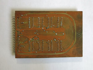
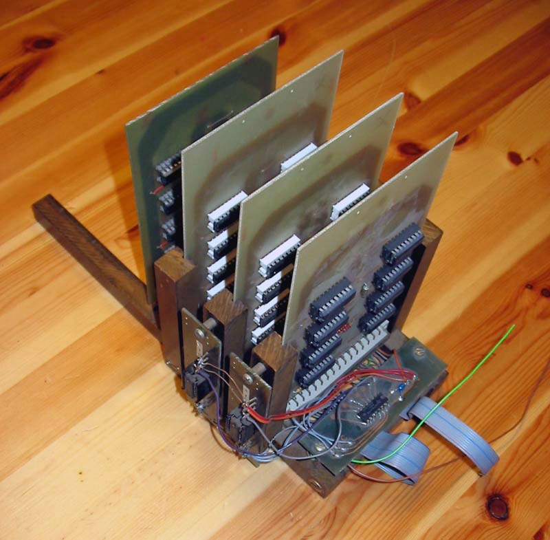
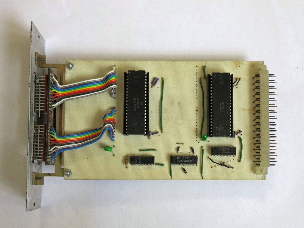
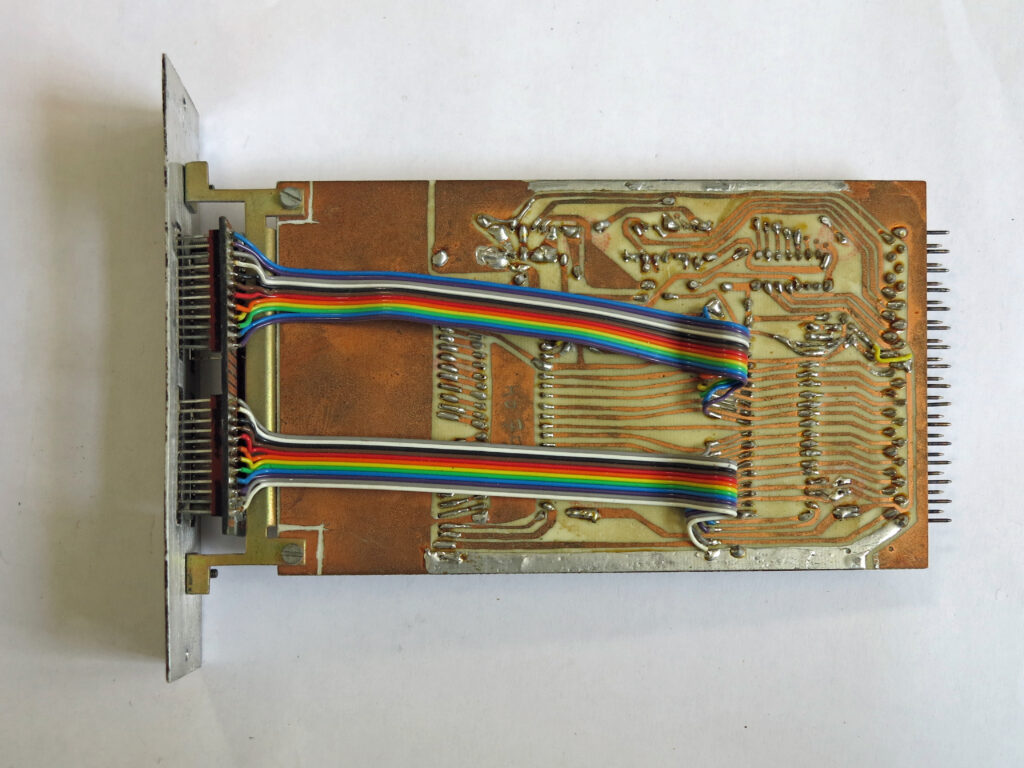
he RAMpager is a MTU banked RAM expansion for the KIM-1: the board supports up to 1MB (that’s three orders of magnitude above more than the original 1152 bytes!) of memory and maps it to a 4KB window placed between 2000h and FFFFh. The window can be mapped to different banks for read and write operations via two control ports.

It supports an optional internal/external backup battery to keep the data in the SRAMs valid across power cycles.

Kempac documents added

The Kempac system now is fully documented!

Proton PIM-1 hex monitor source added

Thanks to Gerben Voort the source of the PIM-1 has been added to the PIM-1 page

Subroutines DUMP to tape

0277   1932             ;        SUBROUTINES BELOW   
0278   1932             ;
0279   1932             ;        SUB TO MOVE SA TO VEB+1,2
0280   1932             ;
0281   1932 AD F5 17    INTVEB  LDA   SAL        
0282   1935 8D ED 17            STA   VEB+1       
0283   1938 AD F6 17            LDA   SAH         
0284   193B 8D EE 17            STA   VEB+2       
0285   193E A9 60               LDA   #$60        ; RTS INST
0286   1940 8D EF 17            STA   VEB+3       
0287   1943 A9 00               LDA   #$00        ; CLEAR CHKSUM AREA
0288   1945 8D E7 17            STA   CHKL
0289   1948 8D E8 17            STA   CHKH
0290   194B 60                  RTS
0291   194C             ;
0292   194C             ;       COMPUTE CHKSUM FOR TAPE LOAD   
0293   194C             ;       RTN USES Y TO SAVEX A   
0294   194C             ;
0295   194C A8          CHKT    TAY                     
0296   194D 18                  CLC
0297   194E 6D E7 17            ADC   CHKL
0298   1951 8D E7 17            STA   CHKL
0299   1954 AD E8 17            LDA   CHKH
0300   1957 69 00               ADC   #$00
0301   1959 8D E8 17            STA   CHKH
0302   195C 98                  TYA
0303   195D 60                  RTS
0304   195E             ;		
0305   195E             ;       OUTPUT ONE BYTE USE Y
0306   195E             ;       TO SAVX BYTE
0307   195E             ;  
0308   195E 20 4C 19    OUTBTC  JSR   CHKT        ; COMP CHKSUM 
0309   1961 A8          OUTBT   TAY               ; SAVX DATA BYTE
0310   1962 4A                  LSR   A           ; SHIFT OFF LSD
0311   1963 4A                  LSR   A       
0312   1964 4A                  LSR   A       
0313   1965 4A                  LSR   A       
0314   1966 20 6F 19            JSR   HEXOUT      ; OUT PUT MSD
0315   1969 98                  TYA           
0316   196A 20 6F 19            JSR   HEXOUT      ; OUT PUT LSD
0317   196D 98           	    TYA           
0318   196E 60                  RTS
0319   196F             ;		
0320   196F             ;       CONVERT LSD OF A TO ASCII
0321   196F             ; 	    AND OUTPUT TO TAPE   
0322   196F             ;
0323   196F 29 0F       HEXOUT  AND   #$0F                               
0324   1971 C9 0A               CMP   #$0A
0325   1973 18                  CLC  
0326   1974 30 02               BMI   HEX1
0327   1976 69 07               ADC   #$07
0328   1978 69 30       HEX1    ADC  #$30
0329   197A             ;
0330   197A             ;       OUTPUT TO TAPE ONE ASCII  
0331   197A             ;       CHAR  USE SUB&#039;S ONE + ZRO   
0332   197A             ;
0333   197A 8E E9 17    OUTCHT  STX   SAVX                                
0334   197D 8C EA 17            STY   SAVX+1
0335   1980 A0 08               LDY   #$08        ; START BIT
0336   1982 20 9E 19    CHT1    JSR   ONE         
0337   1985 4A                  LSR   A           ; GET DATA BIT
0338   1986 B0 06               BCS   CHT2        
0339   1988 20 9E 19            JSR   ONE         ; DATA BIT=1
0340   198B 4C 91 19            JMP   CHT3        
0341   198E 20 C4 19    CHT2    JSR   ZRO         ; DATA BIT=0
0342   1991 20 C4 19    CHT3    JSR   ZRO         
0343   1994 88                  DEY   
0344   1995 D0 EB               BNE   CHT1
0345   1997 AE E9 17            LDX   SAVX
0346   199A AC EA 17            LDY   SAVX+1
0347   199D 60                  RTS
0348   199E             ;
0349   199E             ;		
0350   199E             ;          OUTPUT 1 TO TAPE 
0351   199E             ;          9 PULSES 138 MICROSEC EACH
0352   199E             ;   
0353   199E A2 09       ONE     LDX   #$09        ; 
0354   19A0 48                  PHA               ; SAVX A
0355   19A1 2C 47 17    ONE1    BIT   CLKRDI      ; WAIT FOR TIME OUT 
0356   19A4 10 FB               BPL   ONE1
0357   19A6 A9 7E               LDA   #126
0358   19A8 8D 44 17            STA   CLK1T
0359   19AB A9 A7               LDA   #$A7
0360   19AD 8D 42 17            STA   SBD         ; SET PB7=1
0361   19B0 2C 47 17    ONE2    BIT   CLKRDI      ; 
0362   19B3 10 FB               BPL   ONE2
0363   19B5 A9 7E               LDA   #126
0364   19B7 8D 44 17            STA   CLK1T
0365   19BA A9 27               LDA   #$27
0366   19BC 8D 42 17            STA   SBD         ; RESET PB7=0
0367   19BF CA                  DEX   
0368   19C0 D0 DF               BNE   ONE1
0369   19C2 68                  PLA
0370   19C3 60                  RTS
0371   19C4             ;
0372   19C4             ;
0373   19C4             ;        OUTPUT 0 TO TAPE
0374   19C4             ;        6 PULSES 207 MICROSEC EACH   
0375   19C4             ;
0376   19C4 A2 06       ZRO     LDX   #$06        
0377   19C6 48                  PHA               ; SAVX A
0378   19C7 2C 47 17    ZRO1    BIT   CLKRDI                              
0379   19CA 10 FB               BPL   ZRO1
0380   19CC A9 C3               LDA #$C3
0380   19CC A9 C3       
0381   19CE 8D 44 17            STA   CLK1T
0382   19D1 A9 A7               LDA   #$A7
0383   19D3 8D 42 17            STA   SBD         ; SET PB7=1
0384   19D6 2C 47 17    ZRO2    BIT   CLKRDI
0385   19D9 10 FB               BPL   ZRO2
0386   19DB A9 C3               LDA   #195
0387   19DD 8D 44 17            STA   CLK1T
0388   19E0 A9 27               LDA   #$27
0389   19E2 8D 42 17            STA   SBD         ; RESET PB7=0
0390   19E5 CA                  DEX   
0391   19E6 D0 DF               BNE   ZRO1
0392   19E8 68                  PLA               ; RESTORE A
0393   19E9 60                  RTS
0394   19EA             ;
0395   19EA             ;          SUB TO INC VEB+1,2   
0396   19EA             ;
0397   19EA EE ED 17    INCVEB  INC   VEB+1                   
0398   19ED D0 03               BNE   INCVE1
0399   19EF EE EE 17            INC   VEB+2
0400   19F2 60          INCVE1  RTS

Dump to tape

DUMPT dumps via bitbanging a KIM-1 audio tape file.

Very straight forward well commented source.
See also the user manual, which explains the technique quite well.

0119   1800             ;       DUMP MEMORY TO TAPE 
0120   1800               
0121   1800 A9 AD       DUMPT   LDA   #$AD         ; LOAD ABSOLUTE INST
0122   1802 8D EC 17            STA   VEB
0123   1805 20 32 19            JSR   INTVEB
0124   1808             ;             
0125   1808 A9 27               LDA   #$27         ; TURN OFF DATAIN PB5
0126   180A 8D 42 17            STA   SBD          
0127   180D A9 BF               LDA   #$BF         ; CONVERT PB7 TO OUTPUT
0128   180F 8D 43 17            STA   PBDD         
0129   1812             ;                          
0130   1812 A2 64               LDX   #$64         ; 100 CHARS
0131   1814 A9 16       DUMPT1 LDA    #$16         ; SYNC CHAR'S
0132   1816 20 7A 19            JSR   OUTCHT       
0133   1819 CA                  DEX                
0134   181A D0 F8               BNE   DUMPT1       
0135   181C             ;                         
0136   181C             
0137   181C A9 2A       	LDA   #$2A         ; START CHAR
0138   181E 20 7A 19            JSR   OUTCHT        
0139   1821             ;
0140   1821 AD F9 17            LDA   ID           ; OUTPUT ID
0141   1824 20 61 19            JSR   OUTBT         
0142   1827             ;
0143   1827 AD F5 17            LDA   SAL          ; OUTPUT STARTING
0144   182A 20 5E 19            JSR   OUTBTC       ; ADDRESS
0145   182D AD F6 17            LDA   SAH           
0146   1830 20 5E 19            JSR   OUTBTC        
0147   1833             ;
0148   1833 AD ED 17    DUMPT2  LDA   VEB+1        ; CHECK FOR LAST
0149   1836 CD F7 17            CMP   EAL          ; DATA BYTE
0150   1839 AD EE 17            LDA   VEB+2         
0151   183C ED F8 17            SBC   EAH           
0152   183F 90 24               BCC   DUMPT4        
0153   1841             ;
0154   1841 A9 2F               LDA   #$2F;        ; OUTPUT END OF DATA CHAR
0155   1843 20 7A 19            JSR   OUTCHT        
0156   1846 AD E7 17            LDA   CHKL         ; LAST BYTE HAS BEEN
0157   1849 20 61 19            JSR   OUTBT        ; OUT PUT    NOW OUTPUT
0158   184C AD E8 17            LDA   CHKH         ; CHKSUM
0159   184F 20 61 19            JSR   OUTBT         
0160   1852             ;
0161   1852             ;
0162   1852 A2 02               LDX   #$02         ; 2 CHAR'S
0163   1854 A9 04       DUMPT3  LDA   #$04         ; EOT CHAR
0164   1856 20 7A 19            JSR   OUTCHT        
0165   1859 CA                  DEX                 
0166   185A D0 F8               BNE   DUMPT3   
0167   185C             		
0168   185C A9 00               LDA   #$00         ; DISPLAY 0000
0169   185E 85 FA               STA   POINTL       ; FOR NORMAL EXIT
0170   1860 85 FB               STA   POINTH        
0171   1862 4C 4F 1C            JMP   START         
0172   1865             ;
0173   1865 20 EC 17    DUMPT4  JSR   VEB          ; DATA BYTE OUTPUT
0174   1868 20 5E 19            JSR   OUTBTC  
0175   186B             ;		
0176   186B 20 EA 19            JSR   INCVEB
0177   186E 4C 33 18            JMP   DUMPT2