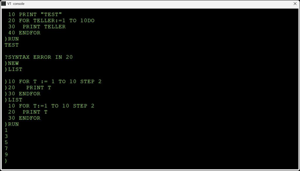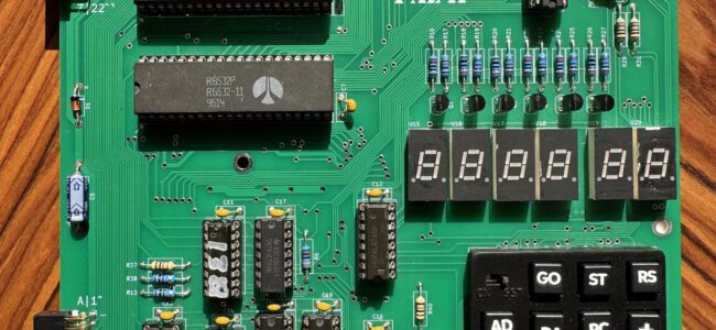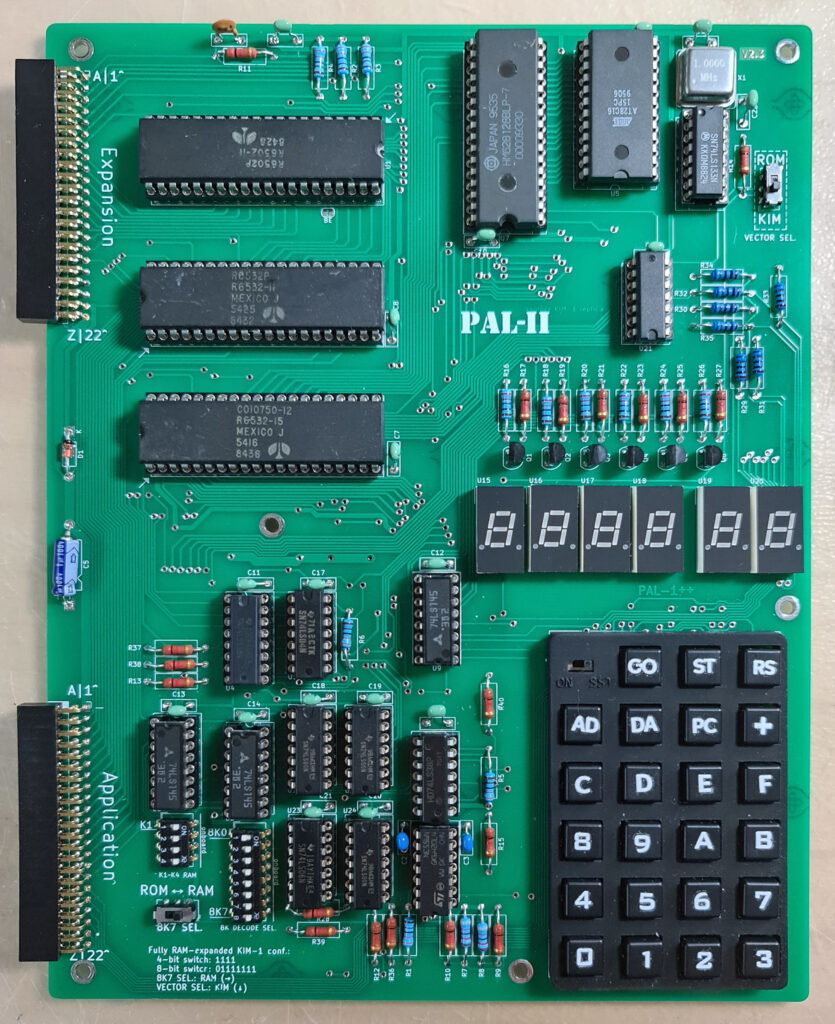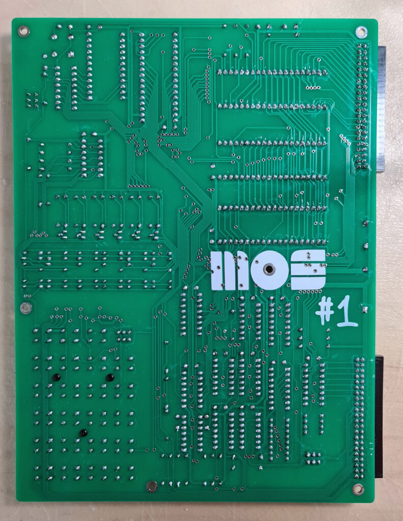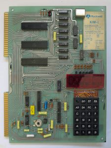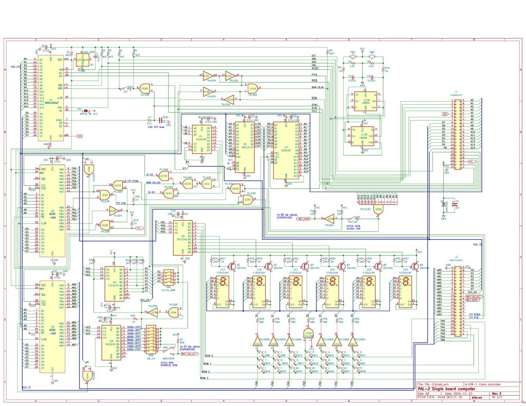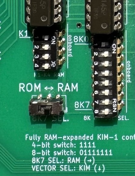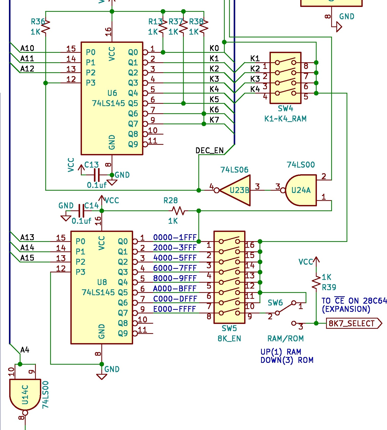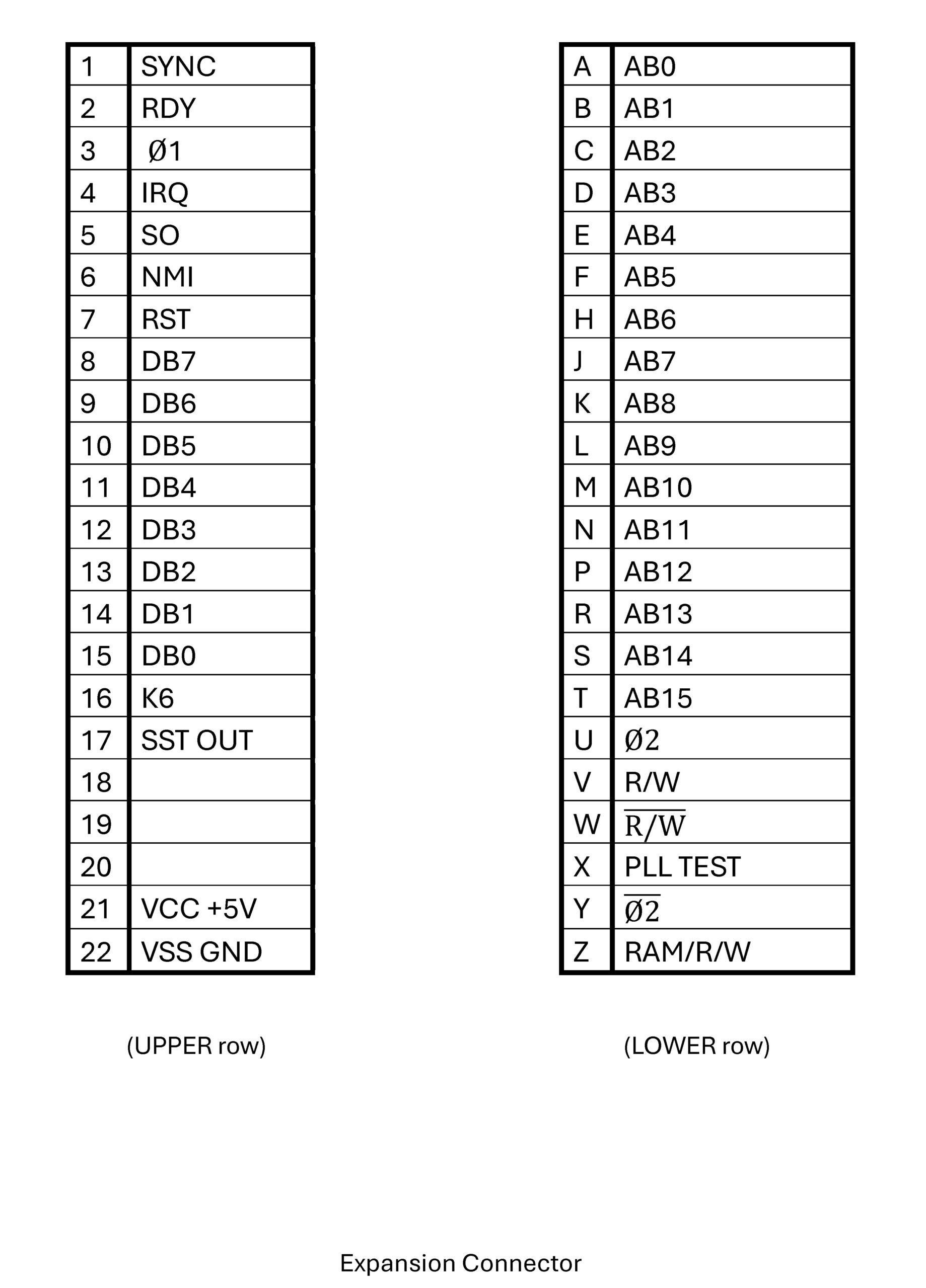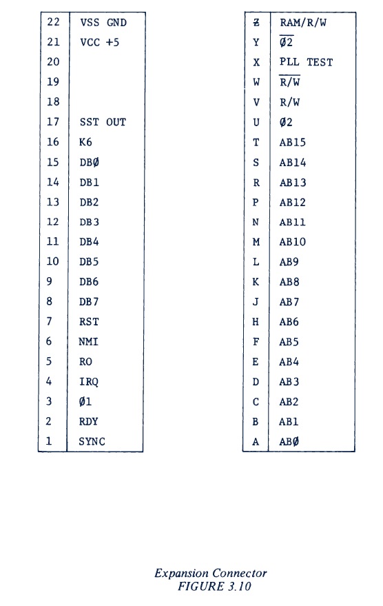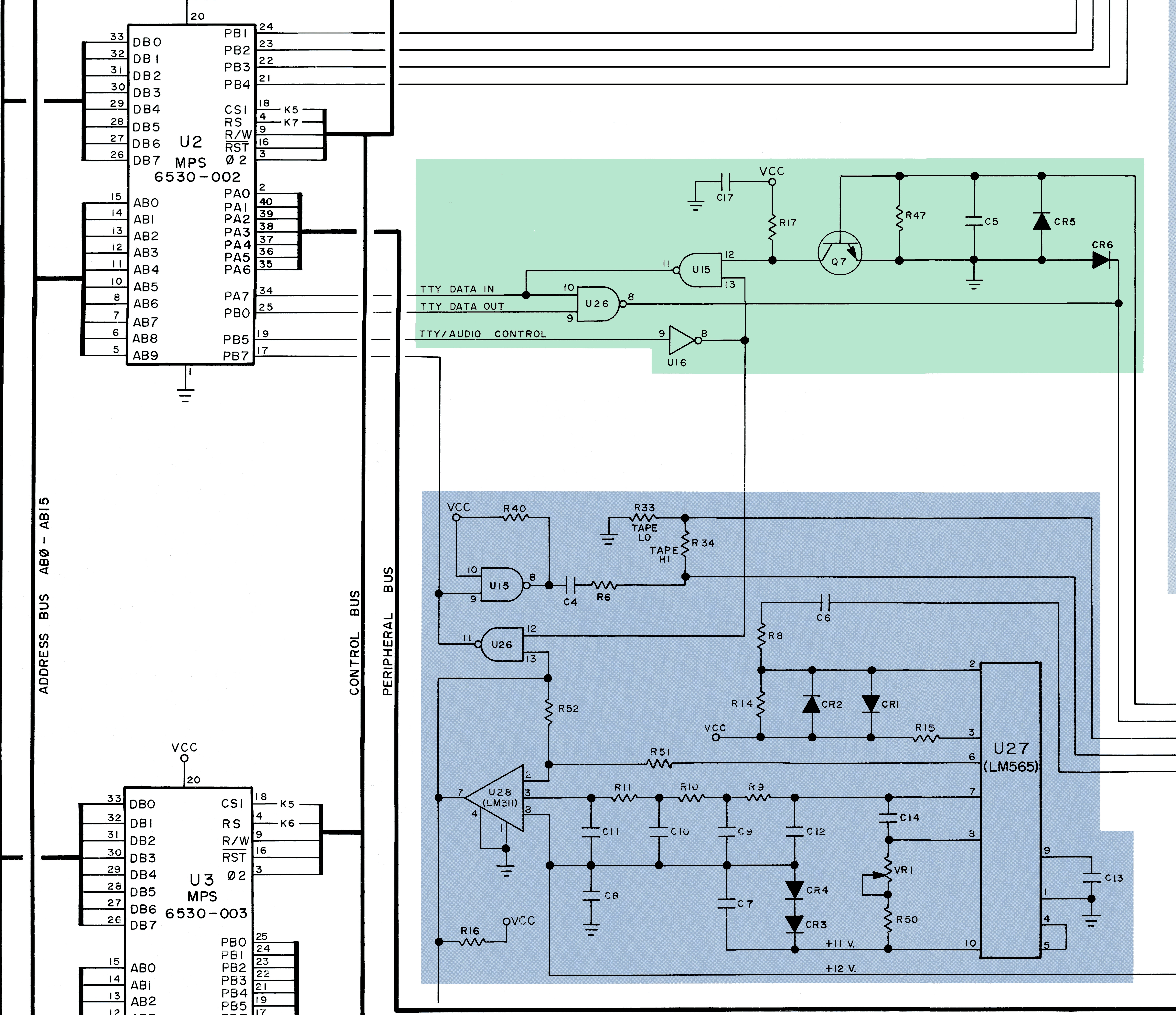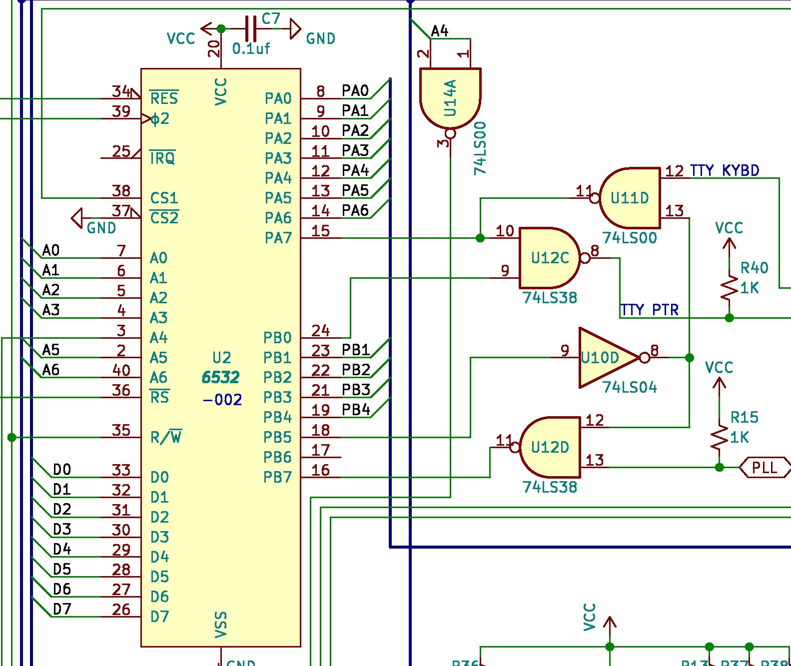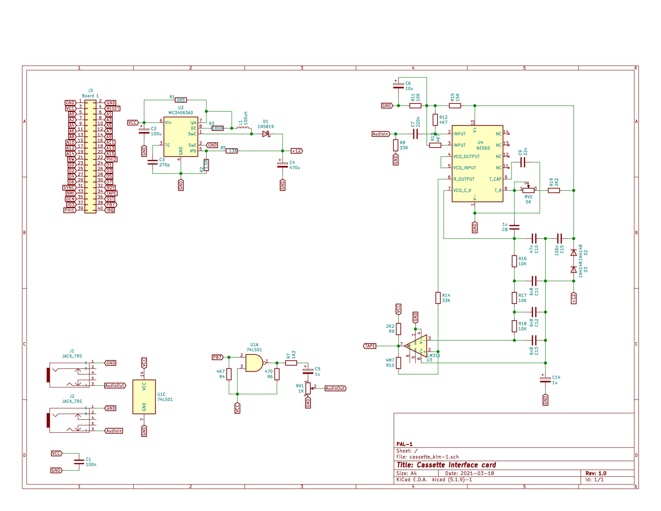
A collection of articles about the KIM-1, original in Dutch, here translated to English and with source and binary of the programs published as listings.
The original articles were scanned from the magazine pages. converted back to text with OCR and translated to English.
The documents in Dutch and English are also published again in PDF format.
If a program listing was included the assembler source is reconstructed in modern MOS Technology syntax. The binary output is compared to the printed binary code and a papertape formatted binary is included.
The articles describing the expansions we designed for our KIM-1s at the magazine are on a separate page.
Downloads available for every article:
– the original scanned article in Dutch
– the Dutch OCR’ed and recreated article
– the English, translated from the OCR result, and recreated article
– an archive with source and binary if applicable
Articles here:
- The KIM-1
- Write your own programs
- Programming step by step
- Mastermind on the KIM
- Morse decoding with the KIM
- Melodiant
- Frequencymeter
- KIM Timer and Clock
- Zero page shifter
- Telex Monitor Program
- Gregorian Clock
- PIA Buffer
- Automatic Register Readout
- Mini-assembler
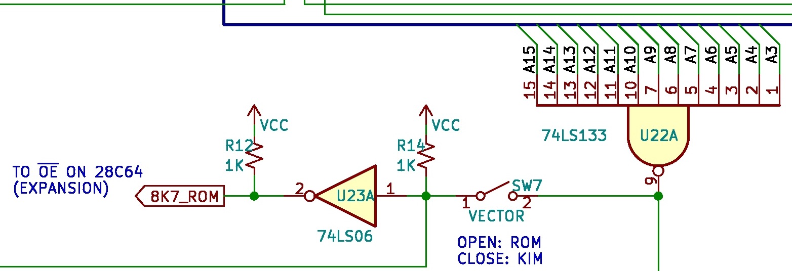
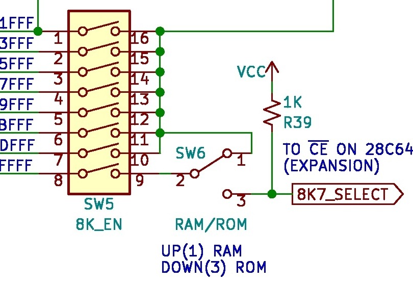
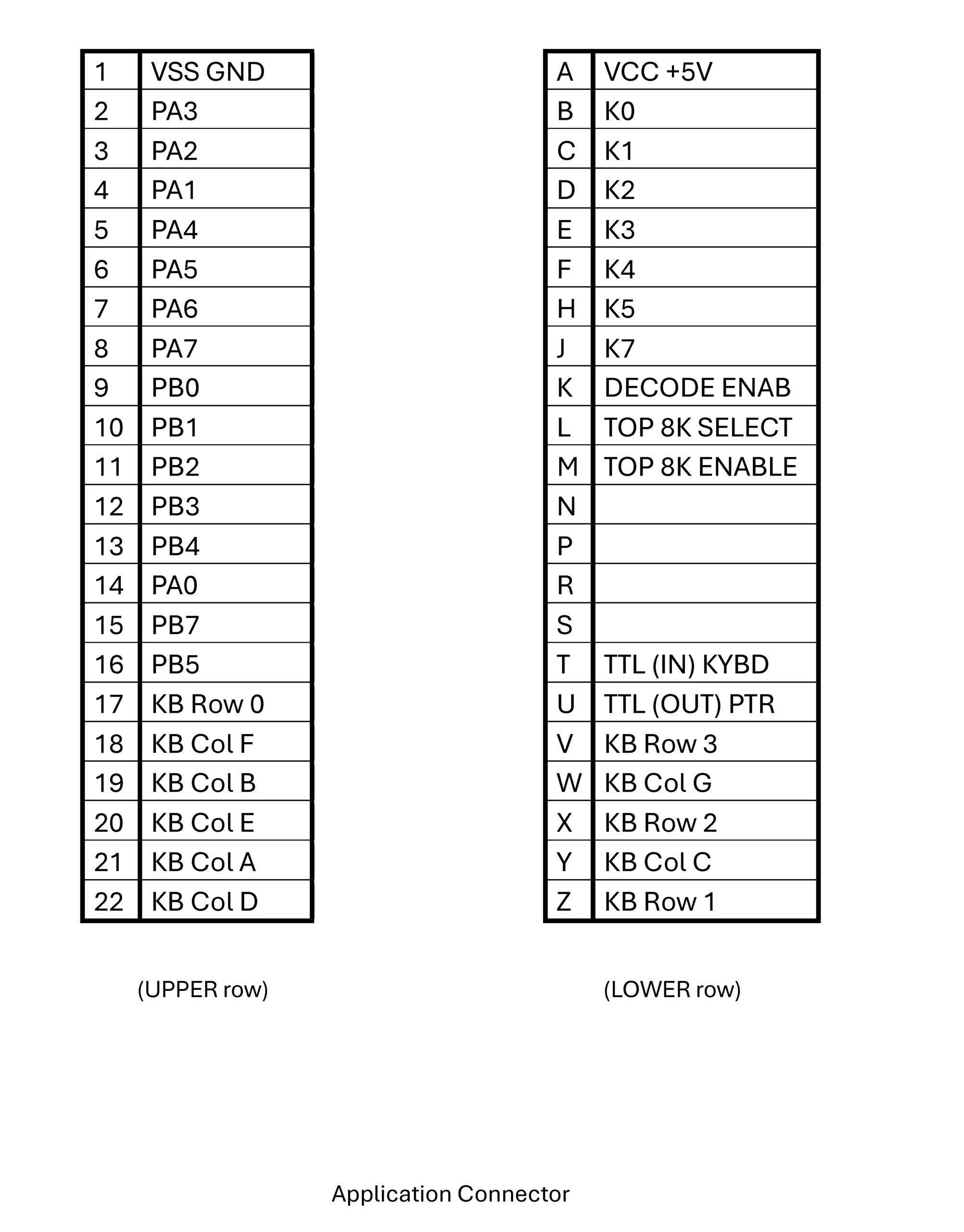
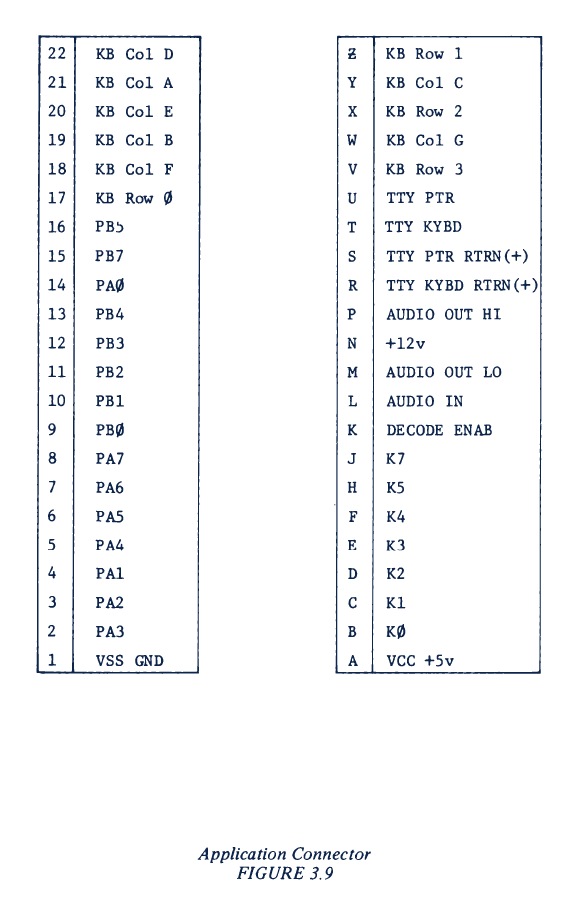
- My KIM-1 expansions in Radio Bulletin
De KIM-1
The article that started the KIM-1 articles!
 |
De KIM-1 Radio Bulletin Augustus 1977 Original article |
|
The KIM-1 RB Aug 1977 English |
|
De KIM-1 RB Aug 1977 Dutch |
Write your own programs
Radio Bulletin September 1977
The most enjoyable work is of course writing your own programs, making the KIM I do exactly what you want. Now, programming is not that easy for someone who has never done it before. Especially at the beginning, the aspiring programmer works in such a disorganised way that in the end he no longer knows which instruction is at which address. It is therefore important to set up a program in a clear, orderly way and to write down every change. In this article we will use an example to show how this is done. However, we leave the exact working-out to the reader, because here too it is certainly true: practice is the best teacher!!!
 |
Zelf programmas maken Radio Bulletin september 1977 Original article |
|
Writing your own programs English RB Sept 1977 |
|
Zelf programmas maken Dutch |
Programming step by step
A five part article in Radio Bulletin 1978 to 1979
Since RB’s KIM campaign in August of last year, the number of KIM owners has grown considerably. Readers’ reactions show that some of the new KIM owners are already getting the hang of programming quite well. Another group, however, is clearly lagging behind: the people who cannot find the ‘beginning’. That is very understandable when you consider that, although the computer is built from electronics, programming is completely new territory for many. In this article RB will therefore try to help this group on their way.
 |
Programmeren stap voor stap Radio Bulletin 1978 to 1979 |
|
Programmeren stap voor stap Dutch |
|
Programming step by step English |
/ |
Programming step by step sources |
Mastermind on the KIM
Radio Bulletin December 1977
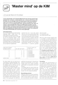
You are probably familiar with the well-known game Mastermind. Normally this game is played by two people, with only one person actively trying to guess a hidden code. The second person has the passive task of indicating, with black and white pegs, whether the chosen colours are correct and whether they are in the right positions. Replace the colours with digits, the black and white pegs with letters, and the KIM takes the place of the passive player. At your command, it chooses a secret colour combination and uses letters to indicate how many digits have been correctly guessed. A special “cheat button” makes it possible to peek secretly behind the screen; the consequence, however, is that the turn counter is increased by 30 points.
Runs on the unexpanded KIM-1 with keypad and seven segment display.
 |
Mastermind on the KIM Radio Bulletin 1977 original scan |
|
Mastermind on the KIM Radio Bulletin 1977 English |
|
Mastermind on the KIM Radio Bulletin 1977 Dutch |
|
Mastermind source and binary |
Morse decoding with the KIM
Radio Bulletin July August 1979
It may be quite nice to be able to say that you are the owner of a microcomputer (if things continue as they are now, in a few years this will be just as commonplace as owning a pocket calculator is today), but even nicer is to also own programs and to be able to spend a number of useful and above all pleasant hours with the device. The following program, written for the KIM, may contribute to this. It makes it possible to display received Morse signals as ‘readable writing’ on the KIM display. Although with a seven-segment display by no means all letters and punctuation marks can be formed, and therefore certain symbols had to be found for these characters, after some practice it is quite possible to read messages sent in Morse code from the display. The program can be used not only for displaying received messages, but also for practising sending and for checking the sending technique. From what is shown on the display one can determine what mistakes are being made while sending
 |
Morse decodering met de KIM July Augustus 1979 original scan |
|
Morse decoding with the KIM July Augustus 79 Radio Bulletin English |
|
Morse decodering met de KIM Juli augustis 1979 Dutch |
|
Morse decoding with the KIM source and binary |
|
Morse decoding circuit in Kicad By Roland van Straten |
Melodiant
Radio Bulletin august 1977. Dick Boer.
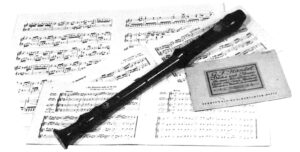
The Melodiant plays a complete melody of up to 256 tones on a command given by you. The display shows which note is being sounded. This makes the Melodiant a very versatile instrument. For example, you can play duets together with the Melodiant by typing in one of the two voices beforehand. The advantage over a tape recorder is that the melody can be played at any desired tempo, which can make practicing easier. What about the Melodiant as a music teacher? A note appears on the display, and the student must try to sing or whistle that note. Afterwards, the loudspeaker can be switched on to check. The Melodiant will also flawlessly play back the most difficult rhythms, slow or fast as needed.
But the possibilities do not end there. We can make the Melodiant play so fast that the individual tones are no longer recognizable. This can produce the strangest sound effects.
 |
Melodiant Radio Bulletin Augustus 1977 original scan |
|
Melodiant August 1977 Radio Bulletin English |
|
Melodiant Augustus 1977 Radio Bulletin Dutch |
|
Melodiant Radio Bulletin Aug 1977 source and binary |
Frequencymeter
Radio Bulletin January 1981 M. Dohmen, R. Koekoek
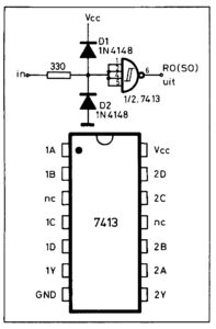
The program described here can measure a frequency up to, mind you, 100 kHz, with a deviation of no more than one cycle in 65536. The frequency is read out in five digits. The program was written for the KIM, but is also well suited to other 6502 microcomputers, notably the SYM and the Junior. Once started, the program measures a frequency continuously when key “6” is pressed, and once when key “0” is pressed.
 |
Frequentiemeter Radio Bulletin Januari 1981/td> |
|
Frequency meter Radio BulletinJanuary 1981 English |
|
Frequency meter Radio BulletinJanuary 1981 Dutch |
|
frequencymeter source and binary |
KIM Timer and Clock, Radio Bulletin May 1980, Herman Perk
While working with the KIM I once encountered the problem that a clock had to be maintained during the execution of a program. Not for the KIM itself, but for a system with the TIM monitor, namely the BEM-bus-based 6502 system from the company Brutech, which is highly recommended for its high quality and well-thought-out design (hence the prices). At the end of 1978, however, both the KIM and the BEM system were still lacking 6522 VIAs with their versatile timers, unlike the SYM and AIM-65. Worse still, the TIM monitor uses the only timer available in the system for communication with the terminal. If I nevertheless wanted to use the 6530 timer for the clock, I had to write my own program for communication, based on the so-called software timing loops. I did so, since I no longer needed TIM itself for the result. As for the timer (those of the 6530 and 6532 are identical), the “obvious” operating instructions say nothing about a possible “free-running” mode as would be usual for a clock and as is described for the 6522
 |
KIM Timer and Clock Radio Bulletin May 1980 Original article |
KIM Timer and Clock May 1980 |
KIM Timer and Clock May 1980 Radio Bulletin May 1980 English |
|
KIM Timer and Clock May 1980 Radio Bulletin May 1980 Dutch |
|
KIM Timer and Clock source and binay |
Zero page Shifter
D.M. de Boer, Augustus 1979 Radio Bulletin
 |
Zero Page shifter Original article |
|
Zeropage shifter August 1979 English |
|
Zeropage shifter August 1979 Dutch |
|
Zeropage shifter RB August 1979 Source and binary |
Telex Monitor Program
Radio Bulletin April June 1981 M.B. Immerzeel
Those who own a “simple” microcomputer such as the KIM or the SYM, and who also own a telex transceiver, will long since have thought about using the telex as a terminal and may already have a program for that purpose. However, most of these programs are limited to noting down addresses with their contents one below the other, and are therefore not particularly economical with paper. The program described below offers the following possibilities:
a. Loading a program in hexadecimal code.
b. Loading ASCII characters.
c. Printing memory contents as hexadecimal numbers.
d. Printing ASCII characters.
e. Starting a program.
 |
Original article Radio Bulletin April June 1981 |
|
Telex Monitor Program Ènglish |
| Telex Monitor Program Dutch |
Telex monitor RB June 1981 dutch |
|
Telex Monitor Program source and binary |
Gregorian Clock
Radio Bulletin May 1981
This clock program is very short and will certainly prove useful to many people. It counts in decimal and keeps track, in decimal, of quarter seconds, seconds, minutes, hours, day of the week, date, month, year and century. Leap years are taken into account!
 |
Gregoriaanse klok Original article Radio Bulletin May 1981 |
|
Gregorian Clock English |
|
Gregorian clock Dutch |
|
Gregorian clock source and binary |
PIA Buffer
Radio Bulletin November 1983
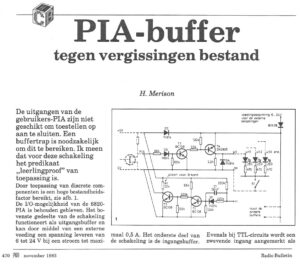
The outputs of the user PIA are not suitable for connecting devices to. A buffer stage is necessary to achieve this. I believe that the term “student-proof” applies to this circuit
 |
PIA-buffer Original article Radio Bulletin November 1983 |
|
PIA Buffer Nov 1983 Dutch |
|
PIA Buffer Nov 1983 English |
Automatic Register Readout
Radio Bulletin February 1978
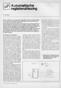
When developing programs on the KIM 1, we can make use of the single-step facility that the KIM has. After each press of the ‘GO’ key, one instruction is executed.
The display then shows the address of the next instruction to be executed. After each step we can check the contents of the various registers. A drawback is that an address has to be entered for each register, which makes checking rather cumbersome. This article describes a program that ensures that, while the ‘GO’ key is held down, the contents of 3 memory locations of your choice appear on the display simultaneously. When the key is released, the address of the next instruction to be executed appears again.
 |
Automatische register uitlezing Orginal article |
|
Automatic Register Readout English |
|
Automatisch Register Uitlezen Dutch |
 |
Automatic Register Readout Source and binary |
Mini-assembler
Radio Bulletin March April 1981
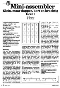
Are you annoyed time and again by having to calculate branch offsets for branch instructions? We are not anymore, because the “Mini-assembler” described here makes programming the KIM considerably easier in many respects. The program itself requires only 254 bytes of RAM/ROM and will therefore be a welcome aid to many KIM users when writing other programs.
 |
Mini-assembler Original article Radio Bulletin March April 1981 |
|
Mini-assembler RB March April 1981 English |
|
Mini-assembler RB March April 1981 Dutch |
|
Mini-assembler RB March April 1981 sources and binaries |