
The RESET of a system with a 6530-004 TIM is a bit special. The RESET code comes from the OTIM ROM, after the RESET the memory map is restored to the documented one.
0084   0000             MDBK   =%00010110        ; X,X,X,PCR,DATA-AVAIL,GOT-DATA,SERIAL-OUT,IN

0095   0000             UINT   =$FFF8

0793   73F8 00 70       INTVEC .WORD NMINT       ; DEFAULT USER INTRO TO NMINT
0794   73FA 00 70              .WORD NMINT
0795   73FC 06 70              .WORD RESET
0796   73FE 52 70              .WORD INTRQ

0144   7006 A9 16       RESET  LDA #MDBK         ; INIT DIR REG, PCR TO 1 RELOCATES
0145   7008             ;
0146   7008 8D 03 6E           STA MDB
0147   700B             ;
0148   700B A2 08              LDX #8            ; X=0
0149   700D BD F7 73    R1     LDA INTVEC-1,X    ; INITALIZE INT VECTORS
0150   7010 9D F7 FF           STA UINT-1,X
0151   7013 CA                 DEX
0152   7014 D0 F7              BNE R1
0153   7016             ;
0154   7016 86 EA              STX MAJORT        ; INIT MAJOR T COUNT TO ZERO
0155   7018 86 E7              STX HSPTR         ; CLEAR HSPTR FLAGS
0156   701A 86 E8              STX HSROP
0157   701C CA                 DEX               ; X=FF
0158   701D 9A                 TXS               ; SP=FF
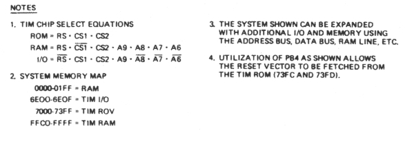
The Chip Select equations for the 6530-004
What is happening here?
The address decoding is a bit course, the ROM of the 6530-004 is not only at $7000, but also mirrored at $7400, $7800 and $7C00. So $73FF is also $7FFF.
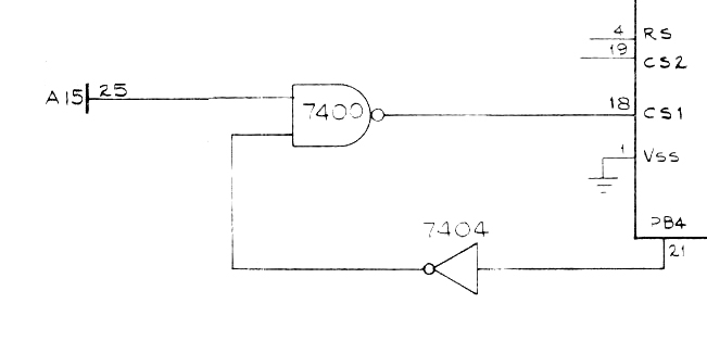
The PB4 circuit from the TIM manual
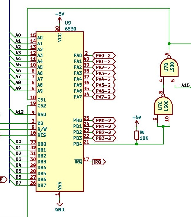
The PB4 circuit in the Jolt, note the pullup resistor.
After power PB4 is an input, the default for a 6530 port. So the inverter input is seen as high (on the Jolt a pullup resistor makes that certain) , so the output of the inverter is low. This blocks the 7400 port input, the other input is A15. So the ROM address $7FFF is mirrored to $FFFF. And so the RESET vector of the 6502 is read from the ROM the 6530-004, and the program counter is set to $7006, the RESET code in the ROM.
The Data Direction register or Port B is loaded with MDBK =%00010110
- 0 PB0 input serial in
- 1 PB1 output serial out
- 1 PB2 is output GOT-Data High speed reader
- 0 PB3 is input DAT-Avail High Speed reader
- 1 PB4 is output PCR this makes PB4 low and A15 reaches the CS of the 6530-004.
- 0 PB5 is input unused
- 0 PB6 is input unused
- 0 PB7 is input unused
By making PB4 an output, PB4 becomes low, the output of the 7400 high, and A15 reaches the 6530, so the ROM is not seen at FFFF. Teh default memory map is now active.
The 8 vector bytes from the ROM are now loaded into the RAM of the 6430-004 at upper memory (location UINT) in a loop with X as down counter to zero (148-152)
Some counters and flags are now initialized to zero with X (High speed reader, serial T count) (154 to 156)
As last the stack pointer is set to $FF (157-158)