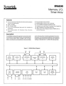
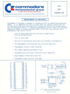
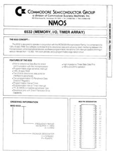
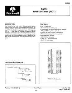
On this page information how to run Tiny Basic, by Tom Pittman, for the KIM-1 or a TIM (RRIOT 6530-004) based machine, like Jolt and Superjolt, with 4K RAM at least extra.
Any 6502 machine with character I/O can run Tiny Basic, source is available with just a few changes to be made to I/O, memory layout and breaktest. Note that most of the zeropage is used by Tiny Basic!
- My work with Tiny Basic
- Tiny Basic manuals
- Downloads binaries, sources for KIM-1 and Jolt/Superjolt/TIM
- Tiny Basic programs
- Magazine articles
- IL Basic Interpreter
- Other sources of information, systems with Tiny Basic
- KIM Kenner article 1980

My work with Tiny Basic
Here I present you with all I own, know and have reconstructed about the 6502 (and 6800) ports of Tiny Basic by Tom Pittman.
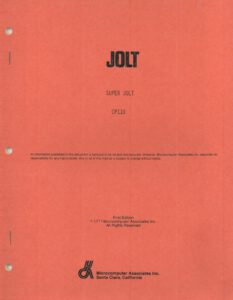
1979 I bought a Tiny Basic package for my KIM-1 from the Dutch distributor Ing Bureau Koopmans for Hfl. 25,- and the package came as a number of documents (User manuals, Getting the most out of Tiny Basic, and the Experimenters kit) and a cassette with two versions of Tiny Basic program in KIM-1 audio format:
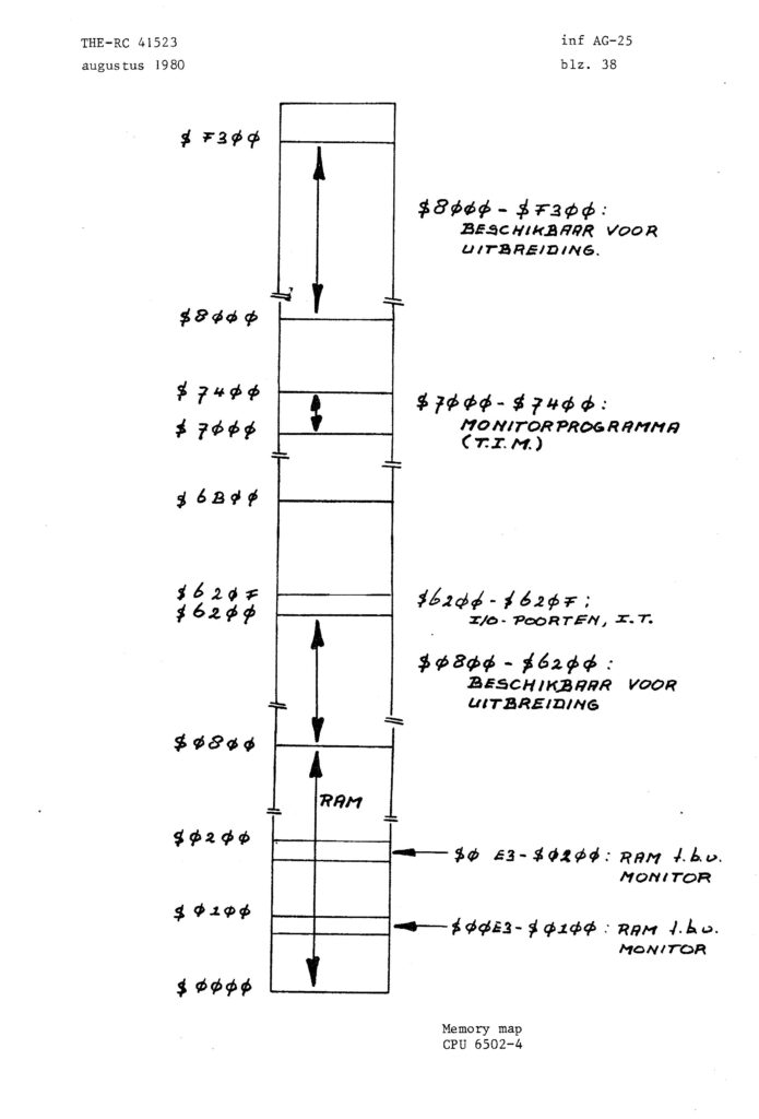
– a low version of the program from 0200 to $0AFF, start address $0200
– a high version from $2000 to $28FF, startaddress $2000
– a Break test routine placed in the lower stack page, $0100-$0114
In 1979 I build a videoterminal (24×32 uppercase monochrome!) and the KIM-1 had 4K memory added in lower memory. So I could use Tiny Basic!
In 1980 I published, in the Dutch KIM Computer Club Magazine KIM Kenner, an article about Tiny Basic, with some patches and tips.
In 2004 I scanned the manuals and dumped the audio cassette wich contained the only remaining Tiny Basic files on cassette. Not the lost original but patched versions as described in the KIM Kenner article I wrote in 1980, reproduced below. I tested those ‘raw’ dumps on the MicroKIM when it appeared as first KIM Clone and it ran more or less. A teletype with papertape punch and reader is not equal to a modern videoterminal.
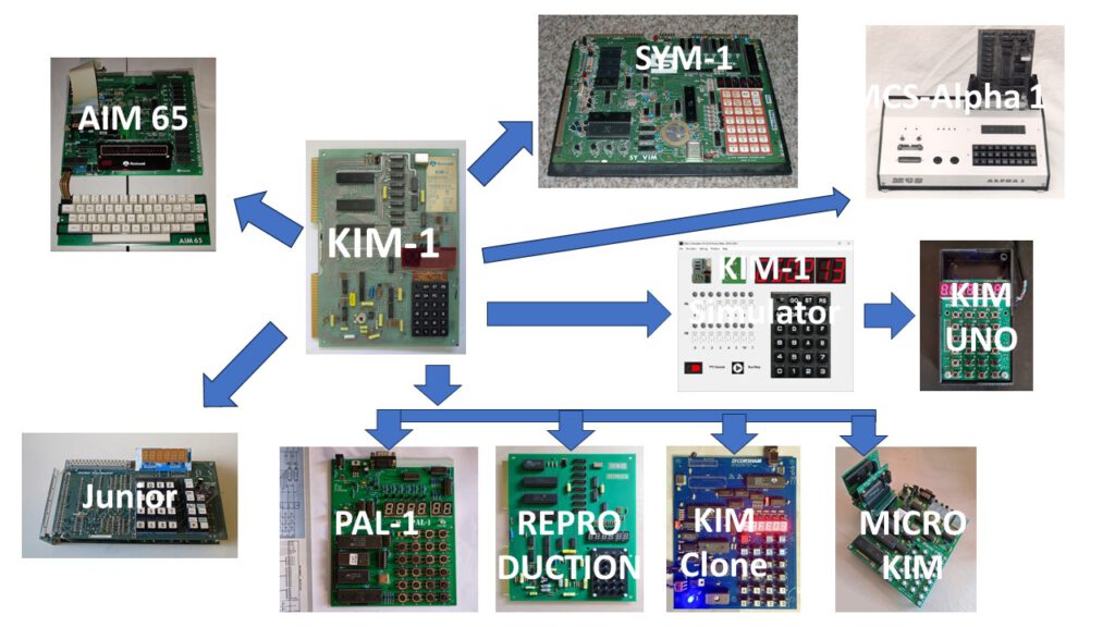
In the years following more KIM Clones appeared such a the Cosham KIM Clone and the PAL-1. And Tom Pittman published some of the material. Other users used my and Tom’s material to let Tiny Basic run on their KIM clone machines. Also sources based on disassembly were constructed.
In 2021 the KIM-1 Simulator was born, that enabled me to dig into programs at the PC.
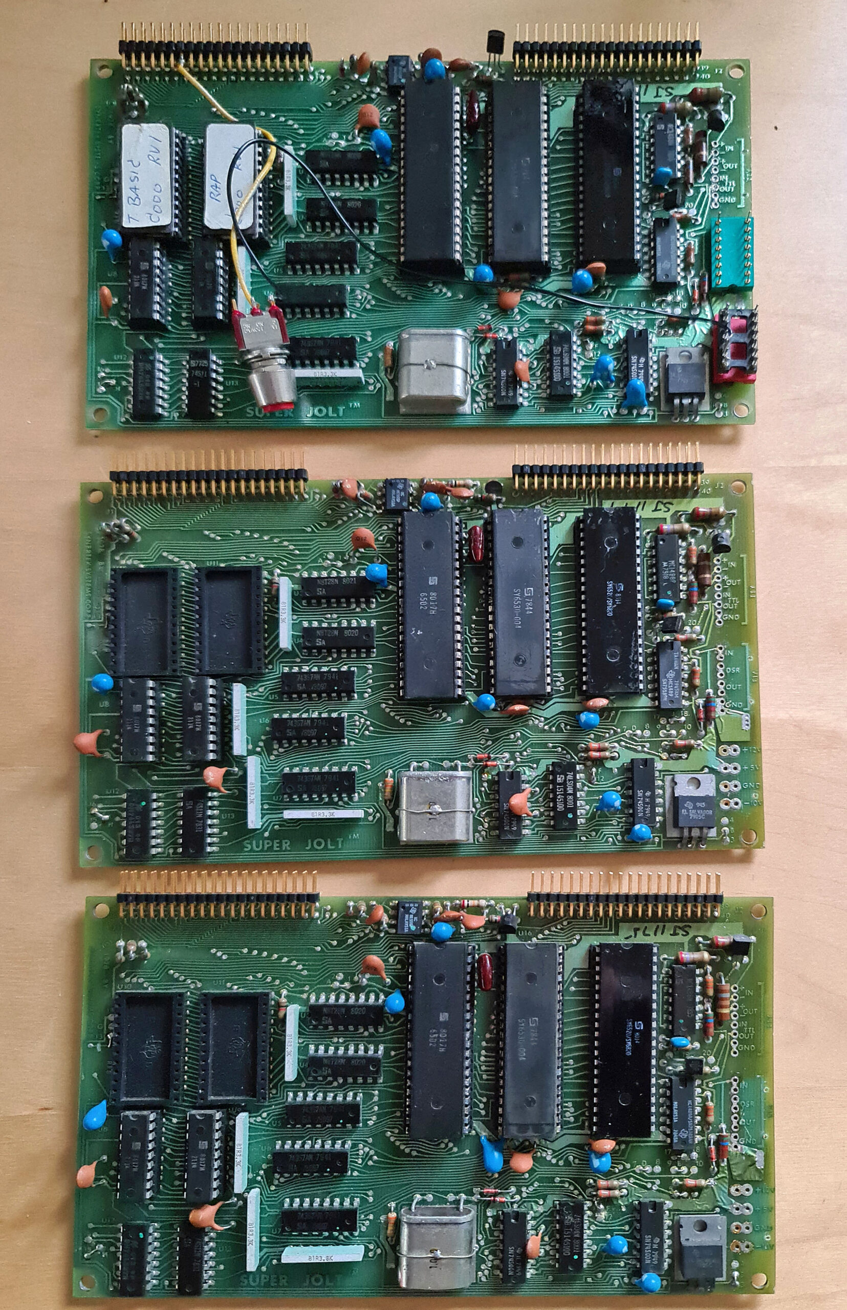
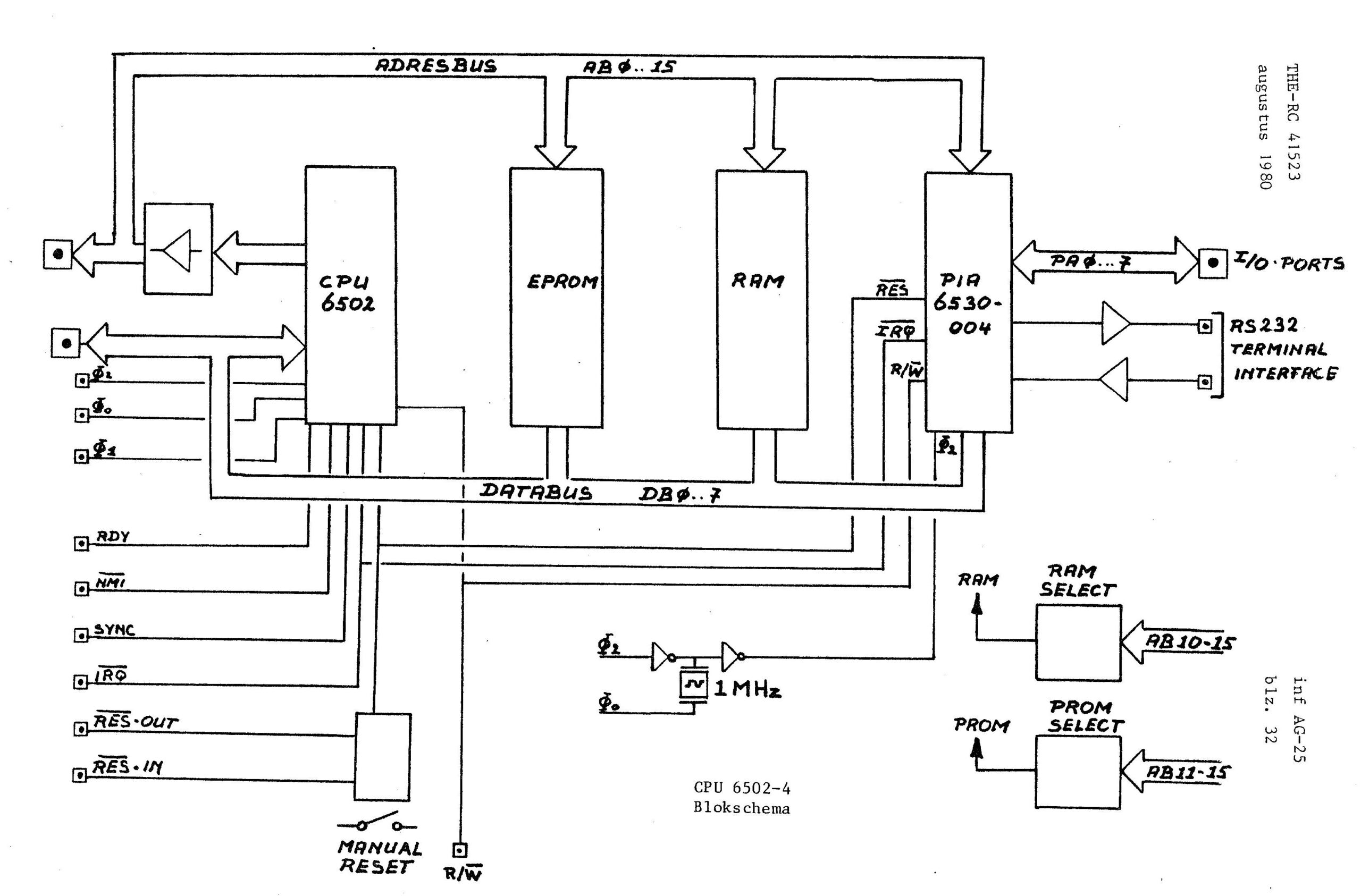
2023 brought me a Superjolt with Tiny Basic in ROM. And that triggered me to build a TIM Simulator. With that I could test and check the Tiny Basic ROM dump. With sources from the website of Tom Pittman I could rebuild the assembler source of Tiny Basic, and check that with the dumps I had of KIM-1 and TIM. You can see the results of that work in the Download section: Tiny Basic can be built for my two platforms on any 6502 system, be it KIM-1, TIM/Superjolt or any 6502 with character I/O. I also found that not all Tiny Basic version come with the same IL Basic interpreter, small differences between KIM-1 and TIM/Superjolt. More on the IL interpreter here
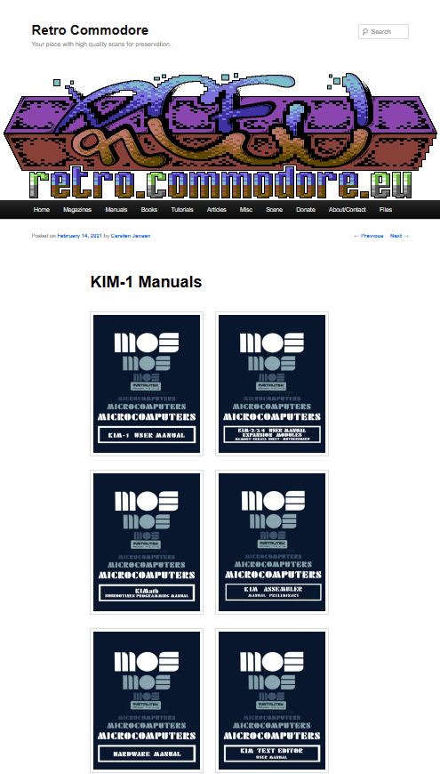
Tiny Basic manuals
The official manuals that came with my version of Tiny Basic. Cleaned up PDF versions 2023.
For a ‘tiny’ language it is very well documented! I have more expensive Basic interpreters without good documentation ..
Downloads of binaries and sources for KIM-1 and TIM/Superjolt
From the manual on the KIM-1:
It is recommended that you save a copy of memory on tape (0100-0114 and 0200-0AFF) before going any further. Or you may prefer to save it on audio cassette. Set up the starting address for Tiny at 0200, and type “G”. Because of the awkwardness of putting memory in the 4K gap left in the KIM-1 system, an alternate version is available which executes out of 2000-28FF. For this version the Cold Start is at 2000 and other addresses are at 200x instead of 020x (cf. 010x in Appendix D).
Tiny Basic binaries and sources for the KIM-1
– raw dump contains the dump of the only remaining audio cassette files in my library.
Dumps made in 2004, lightly patched versions.
– patched original binaries: extracted from the raw dumps as described in the user manual
– original reconstructed binaries, source versions, binaries checked against the original dump with the patches removed
– patched versions , for practical use on a KIM-1 or clone with a modern video terminal emulator.
Sources and papertape included.
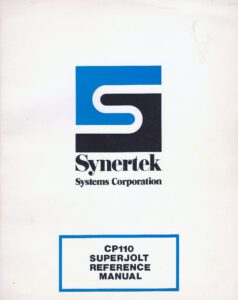
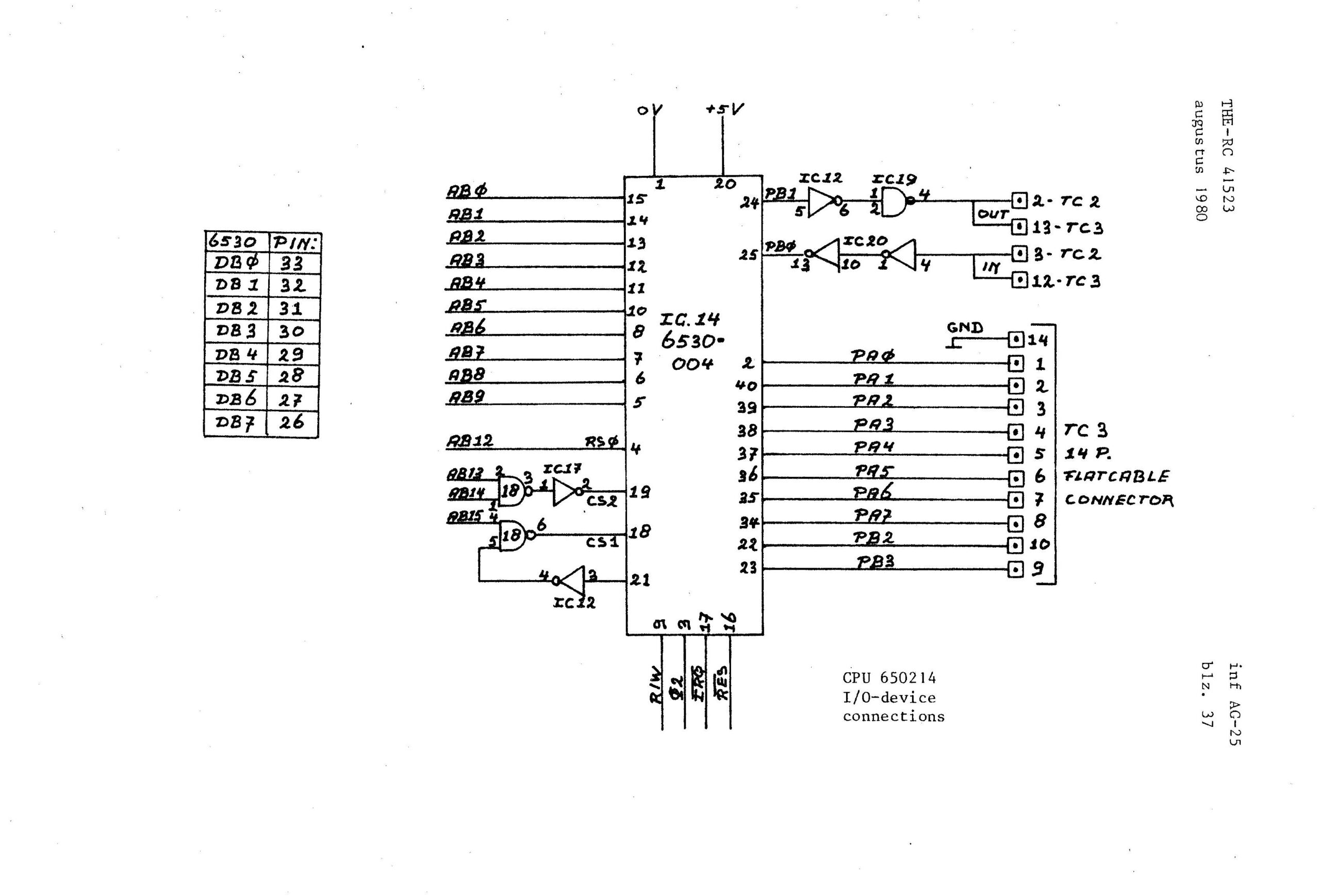
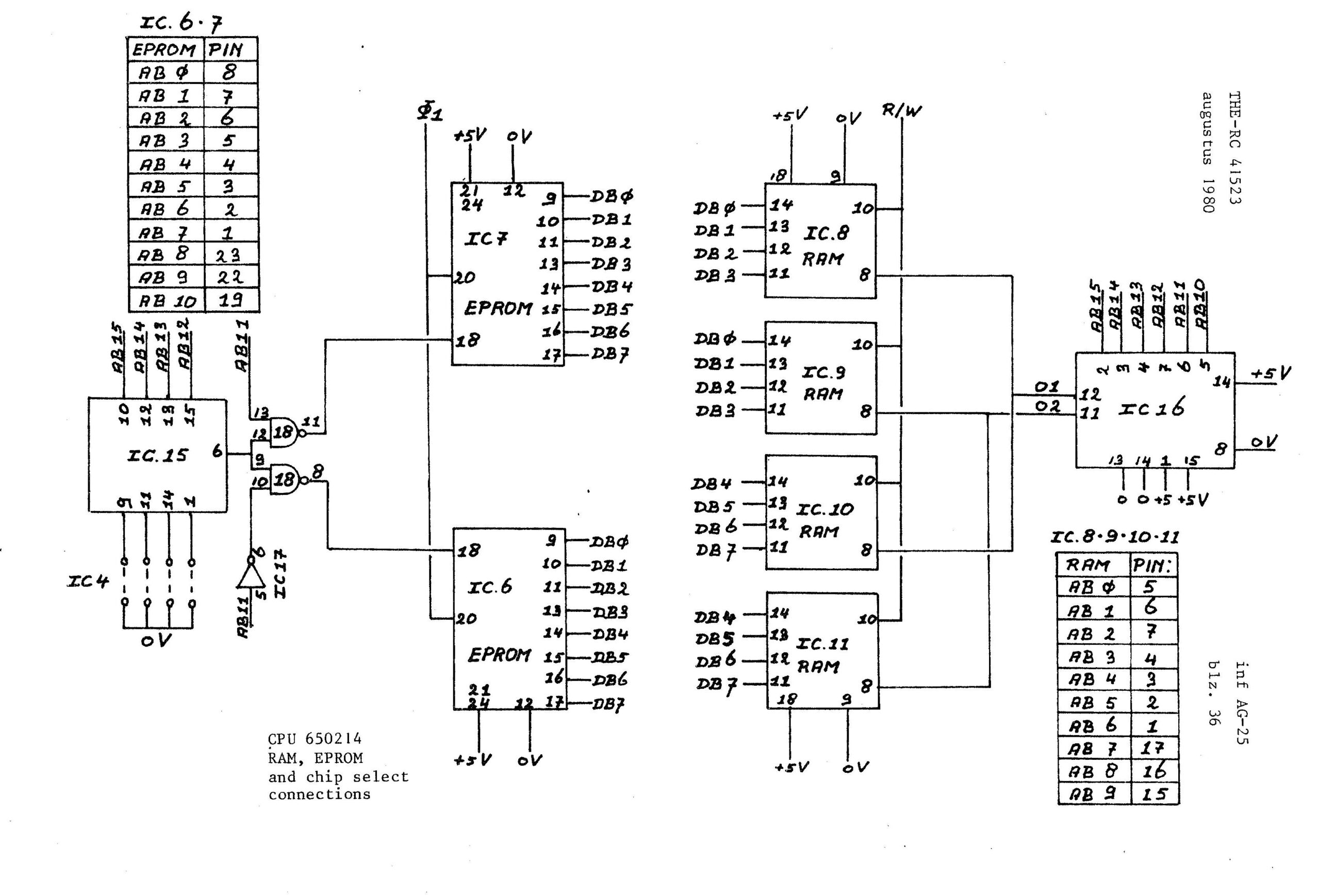
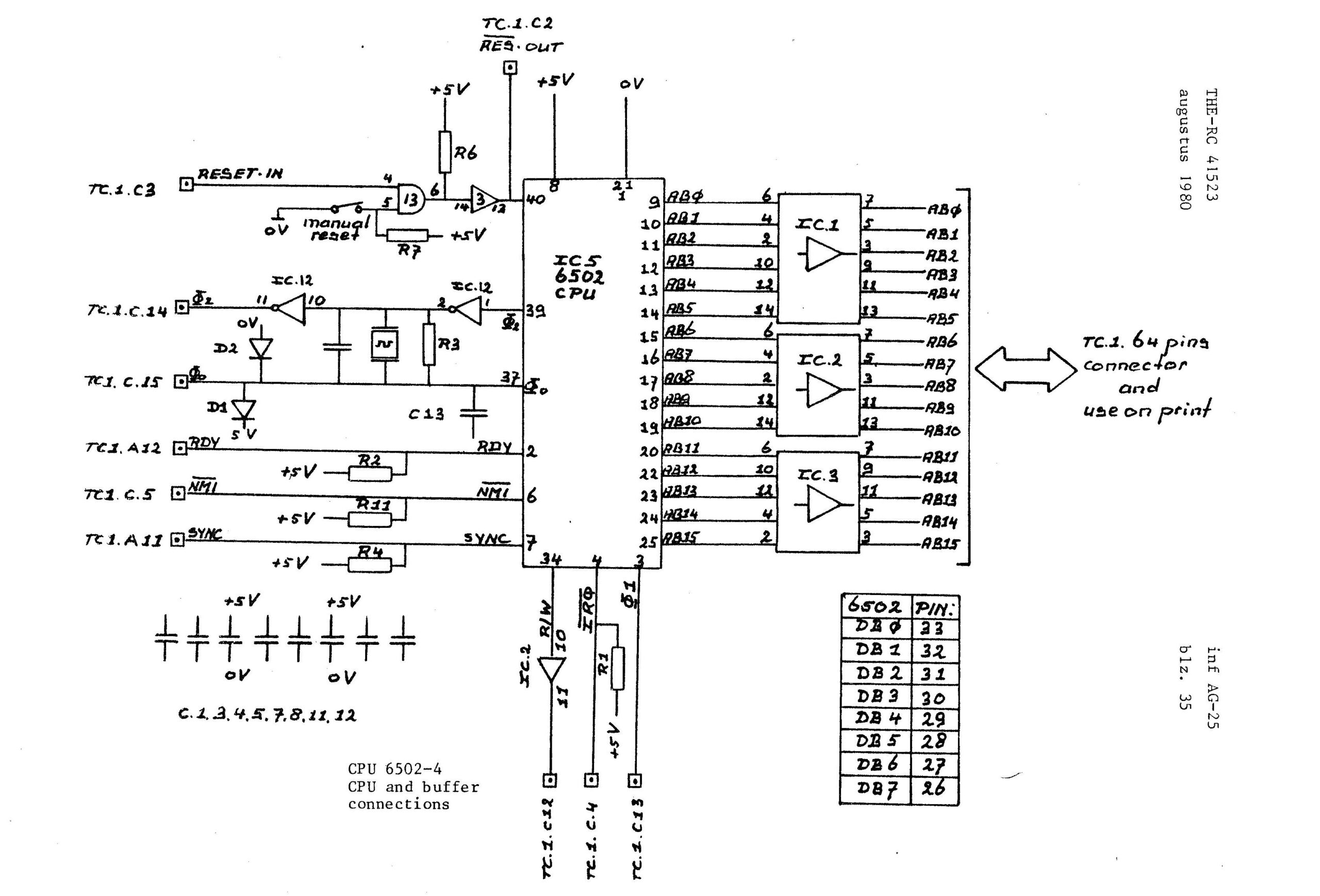
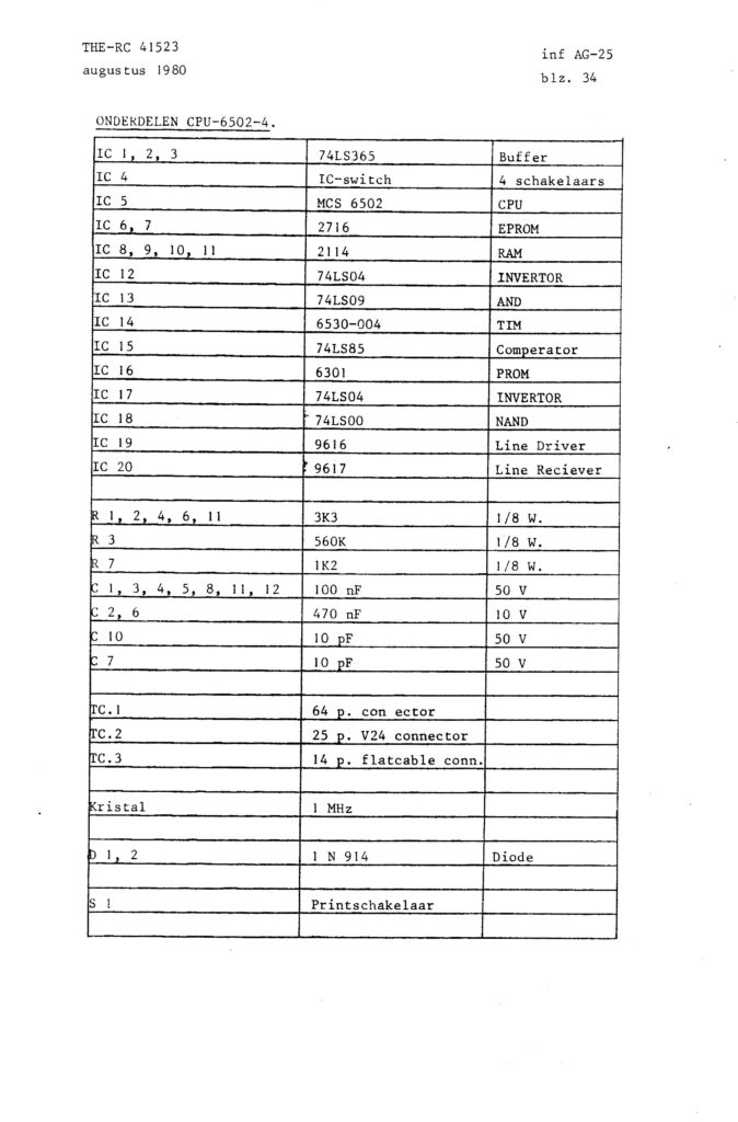
Tiny Basic for the TIM 6530-004 as used in the Jolt and Superjolt. All with sources and binaries..
– original ROM dumps from the Superjolt
– source and checked binaries reconstruction
– patched for more practical use, source and binaries for Superjolt and TIM
– reconstructed version of Tiny Basic for TIM as described in the User manual
Software
Tiny Basic for CC65 assembler sources
Tiny Basic programs, such as adventure
Bill O’Neill source of Tiny Basic with monitor
Tiny Basic source by Bob Applegate
Tiny Basic for the Cosmac 1802 by Robert Coward
Magazine articles
IL interpreter
Tiny Basic is implemented like an onion:
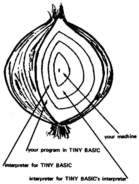
The concept of Tiny Basic was thought of by the people behind PCC magazine, which evolved ito Dr Dobbs. A compact Basic interpreter written in the IL language, which in turn is interpreted in native code. This means lot of functionality in a small space. And porting to other computers means only having to rewrite the quite simple IL interpreter.
Tiny Basic by tom Pittman is such a ported Tiny Basic. For 1802, 6502 and 6800 CPU systems. Note that there are small differences between versions of the IL code. The code for TIM is different for example of the KIM-1 versions.
Other sources of information on Tiny Basic
Information on the Itty Bitty Computers Tiny Basic for the Cosmac here, by Herb Johnson.
Tiny Basic interpreters 6502, 1802, 6800, IL
Tiny Basic for the Cosmac 1802 source, by Robert Coward
6800 source reconstructed by Jeff Trentor.
Tiny Basic for the 6800 hex dumps and source reconstruction
The dialects of Tiny basic
Tiny Basic debugging
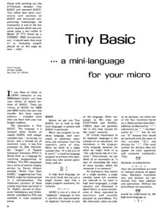
English version of article ‘Tiny Basic’
H.J.C. Otten, KIM Kenner 10 March 1 1980, page 10
With improvements on the Dutch article from unpublished handwritten notes, 1980
Tiny Basic
Tiny Basic deserves more appreciation as programming language than the low price makes us wonder.
(Note 2023; All software for the KIM-1 is free nowadays!)
The following article some advantages and disadvantages wil be described followed by some tips for improvements and ease of use.
Advantages of Tiny Basic
The program is small, 2.5K RAM besides zeropage is enough for the software.
Tiny Basic uses the KIM-1 I/O with the built-in KIM-1 character I/O routines. And of course a TTY like a videoterminal.
Tiny Basic comes in two versions. A low memory version for a KIM-1 with RAM at $0000 – $0ABF and program storage at $B000.
The high memory version starts at $2000, and program storage above.
There are no differences between the low and high memory version besides memory locations.
All I/O of Tiny Basic uses three well defined and documented subroutines, adaptation to other 650 systems requires no more adaptations.
The extensive documentation makes all clear.
Tiny Basic has two start addresses. The Cold start does a complete initialization like a clean program space. The Warm Start keeps the Basic program in memory intact.
Besides the Basic statements there is the USR function to call external 6502 code. The USR function is powerful. The first argument is the address of the 6502 routine.
The second argument, a 16 bit integer, is placed in the X (high) and Y (low) register. The third argument, an 8 bit value, in the Accumulator..
The result of the function result is the accumulator.
Tiny Basic works with 16 bit integers, signed. There are USR calls for peek and poke function.
Disadvantages of Tiny Basic
Any Basic interpreter has known disadvantages. Tiny Basic adds having only 16 bit signed integers, no floating point numbers. No string functions, no FOR .. NEXT, GOTO required, 26 variables max. And Tiny Basic is slow due to the architecture of an interpreter written in the IL interpreter.
Tip 1: Patches go improve usability on video terminals
– The “:’ used as prompt can be replaced with another character. I like ‘>’ as prompt.
– The second patch involves suppressing the video terminal unfriendly output of (un)printable characters.
– Third the backspace character $5F is better replaced with $08 for video terminals.
– The last patch increases the maximum stack depth from 40 to $20.
Patches to apply at Tiny Basic (low version 0200 and high version 2000):
Change location $0971 ($2771) to $3E (‘>’ , was ‘:’ $3A)
Change location $0211 ($2011) to $00 to suppress padding (was 84, padding on in bit 7, 4 times)
Change location $020F ($200F) to $08 (backspace) was $5F
Change location 0213 ($2013) to $20 for more stack space depth (was $04)
Tip 2: Load and save of Tiny Basic programs
There are no Load and Save statements in Tiny Basic.
But it can be done with the following procedure on the KIM-1:
Save your program
1. Halt your Tiny Basic with Reset
2. Copy the contents of $24 to EAL $17F7 (end of Tiny Basic Program storage)
3. Copy the contents of $25 to EAH $17F8
4. Fill SAL $17F5 with $00
5. Fill SAL $17F5 with $0B (0200 version) or $29 (2000 version)
6. Enter tape ID in $17F9
7. G $1800 to save to tape (or a more applicable hypertape routine)
Load a program from tape
1. Start Tiny Basic Cold start (G 0200 or G 2000)
2. Halt your Tiny Basic with Reset
3. Enter ID in $17F9
4. G $1873 to load tape to memory
5. Copy the contents of EAL $17F7 to $24(end of Tiny Basic Program storage)
6. Copy the contents of EAH $17F8 to $25
7. Start Tiny Basic with warm start G $0203 or G $2003
Since the KIM-1 monitor does not allow to use the tape load/save routines as subroutines, making this a program is not much more friendly than the manual operations.

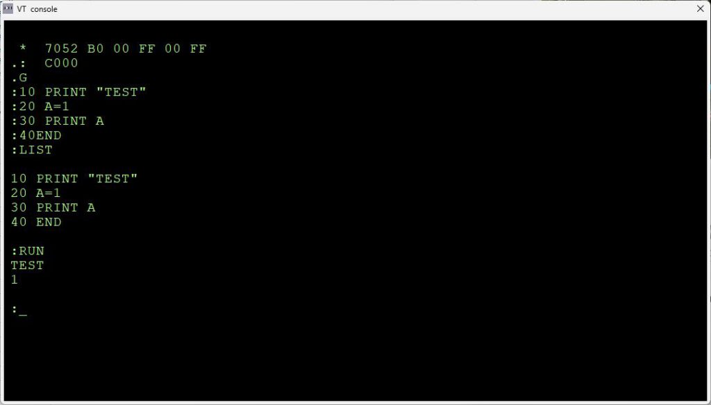


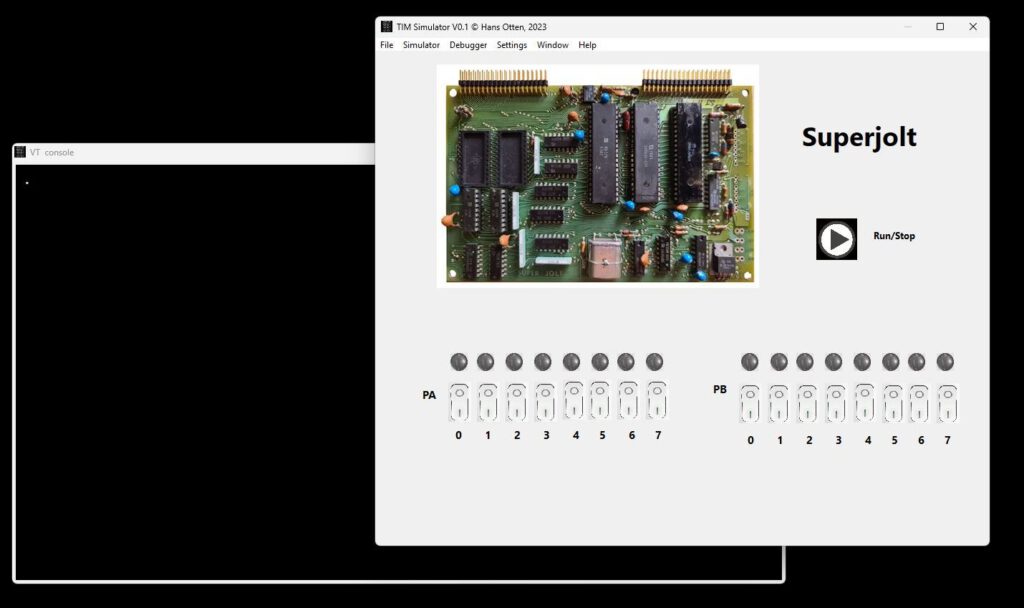
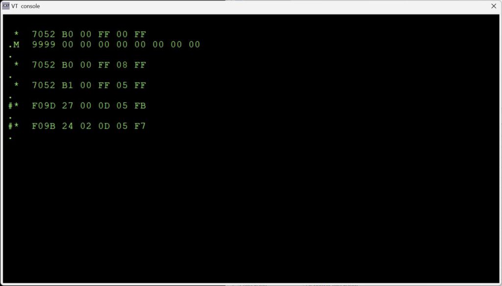 TIM Superjolt Simulator V0.4, Tiny Basic working!
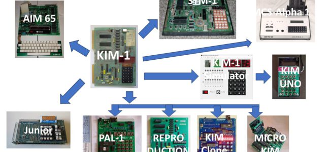