
Replace the 6530-002 and -003 in a KIM-1: a KIM-1 clone.
The base for all ‘modern’ KIM clones, KIM reproductions, MICRO KIM, PAL-1 and more.
Credits to Ruud Baltissen for the idea and details. ‘I’ means Ruud in this page!
RRIOTs are mask programmed for address selection, choices are:
Pin 18 PB6 or CS1
Pin 19 PB5 or CS2
Pin 17 PB7 can have a pullup
ROM selection on RS0, CS1 und CS2 s
RAM on RS0, CS1, CS2, A9, A8, A7 and A6
I/O on RS0, CS1, CS2, A9, A8, A7 and A6
See the various 6530/6532 datasheets for (some) more detail.
The troublemaker: 6530, detailed background information
The KIM-1 has two 6530s on board. For more info about this IC, please read the datasheet. Anybody who is a little bit familiar with the hardware market can tell you that you cannot buy the 6530 anymore. Happily enough there is another IC available which you could call its brother: the 6532. The 6532 has 16 I/O-lines, an internal timer and 128 bytes of RAM on board, but no ROM. The internal ROM of the 6530 can be selected independently from the I/O. So for this project we’ll use an external EPROM as replacement. The pin out of the 6532 is completely different but that should not be a problem.
The next difference is the fact that the 6532 has a separate IRQ and PB7 line. As we will see, the functionality of both lines is the same as with the 6530. To create the same circumstances we only have to connect them together.
The third difference is the availability of PB6 with a 6532. See it as a bonus as I haven’t found any reason how it could jeopardize our project.
The fourth difference is that it is possible to generate an interrupt depending on the behaviour of PA7. But this is an option, which is out of function by default after a reset.
The last and major difference however lays in the way the registers are selected:
function:       RS:  A6:  A5:  A4:  A3:  A2:  A1:  A0:  R/W:

RAM              0    x    x    x    x    x    x    x    x

DRA              1    x    x    x    x    0    0    0    x     A
DDRA             1    x    x    x    x    0    0    1    x     B
DRB              1    x    x    x    x    0    1    0    x     C
DDRB             1    x    x    x    x    0    1    1    x     D

PA7, IRQ off,
      neg edge   1    x    x    0    x    1    0    0    0     F
PA7, IRQ off,
      pos edge   1    x    x    0    x    1    0    1    0     G
PA7, IRQ on,
      neg edge   1    x    x    0    x    1    1    0    0     H
PA7, IRQ on,
      pos edge   1    x    x    0    x    1    1    1    0     I

read interrupt
       flag      1    x    x    x    x    1    x    1    1     E

read timer,
       IRQ off   1    x    x    x    0    1    x    0    1     J
read timer,
       IRQ on    1    x    x    x    1    1    x    0    1     K

Clock / 1,
       IRQ off   1    x    x    1    0    1    0    0    0     L
Clock / 8,
       IRQ off   1    x    x    1    0    1    0    1    0     M
Clock / 64,
       IRQ off   1    x    x    1    0    1    1    0    0     N
Clock / 1024,
       IRQ off   1    x    x    1    0    1    1    1    0     O

Clock / 1,
       IRQ on    1    x    x    1    1    1    0    0    0     P
Clock / 8,
       IRQ on    1    x    x    1    1    1    0    1    0     R
Clock / 64,
       IRQ on    1    x    x    1    1    1    1    0    0     S
Clock / 1024,
       IRQ on    1    x    x    1    1    1    1    1    0     T

In total 5 address lines are used, meaning 32 registers.
But 11 of the 19 registers have one or more mirrors.
Read:        J E J E       K E K E       J E J E       K E K E
Write:       F G H I       F G H I       L M N O       P R S T
R/W:         A B C D       A B C D       A B C D       A B C D
As we can see, the last 16 registers equal the 16 of the 6530 itself.
So now we have to develop some logic which will do the following:
- The 6532 is only visible within a range of 128 bytes
- The first 16 bytes represent register 16 to 31
- The next 48 bytes are mirrors of the first 16
- The last 64 bytes appear as RAM
Conclusion:
- Input A6 won’t be used and can be tied to GND
- Input A4 is connected to address line A4 of the 6502 via an inverter.
- A 74LS138/74LS08 construction or equivalent enables the RS- and CS-lines at the right moment.
ROM and RAM
Here we have a luxury problem. We only need 2K of (EP)ROM like the 2716. The problem is that the 2716 is hard to find and more expansive then the 2764 or its bigger brothers. When we use a bigger EPROM we only have to tie the unused address lines to GND. The same problem occurs with the RAM.
If we have to use bigger RAMs or EPROMs anyway, it is quite easy to use other parts of that chip by OR-wiring the CS-line with more Kx-outputs of the main 74145. (Don’t forget the address lines!) In case of the EPROM we also can tie switches to the surplus address lines and have the advantage of a multi-KERNAL system.
Schematics of the new KIM-1
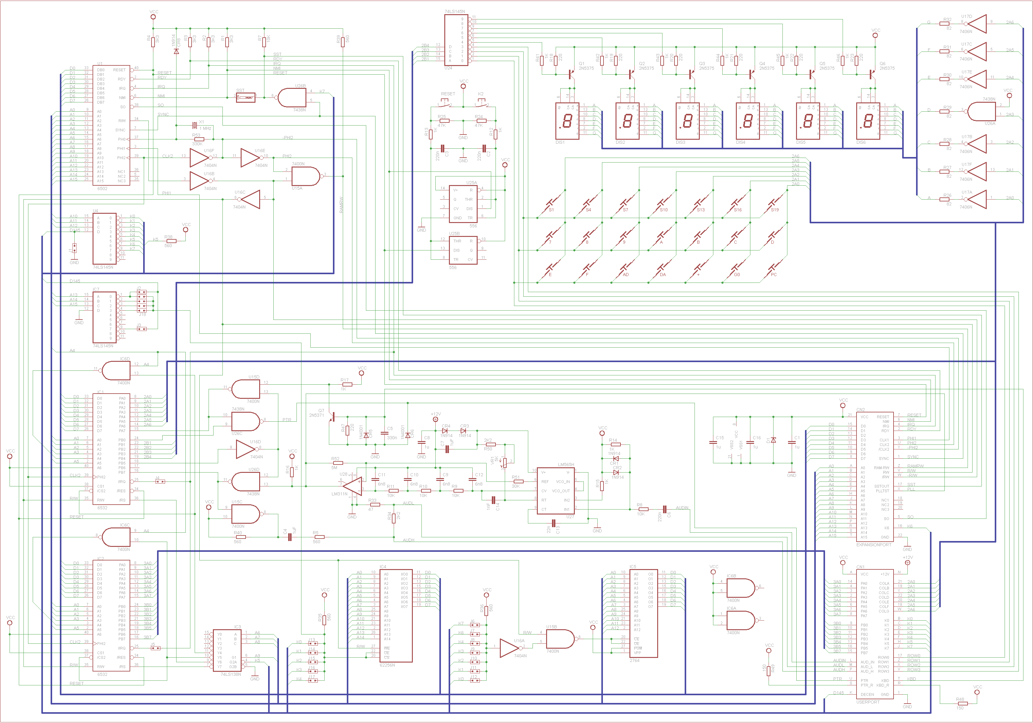
What are the major differences with the original circuit:
- Replacement of the 6530s by 6532s.
- Replacement of the 6108 RAM-ICs by one 6264 or equivalent 8K*8 SRAM.
- Adding an EPROM.
- Adding a 74LS138 to decode the RAM and I/O of the 6532s.
- Combining K6 and K7 to one line, dropping the resistor for K6.
- Adding jumpers to enable combining other K-lines as well.
You may notice that Ruud did not change things which are more or less obvious like replacing the clock circuit by a module or replacing the various 74XX TTL-ICs by their LS or HCT equivalents.
6530’s KIM-1 specification
(Thanks to J Coville)
Back in the day, a designer ordering a custom 6530 would have to specify certain parameters in addition to the ROM contents. During my KIM-1 restoration effort, I found a datasheet for the Synertek version of the part. The datasheet has quite a bit of information describing how to provide the ROM contents. There is also a form for “Additional Pattern Information” (tables to describe the desired chip-select and addressing information). They look like this:
Chip Select Code (Check one square in each block)
|
|
|
|
ROM/RAM/I-O SELECTS (Specify H or L or N (don’t care) in each box.)
| RS | CS1 | CS2 | A9 | A8 | A7 | A6 | |
| ROM Select | N | N | N | N | |||
| RAM Select | |||||||
| I/O Select |
As best as I can determine, the designers of the KIM-1 filled out the tables for the RRIOTs like so:
6530-002:
|
|
|
|
| RS | CS1 | CS2 | A9 | A8 | A7 | A6 | |
| ROM Select | L | H | N | N | N | N | N |
| RAM Select | H | L | N | H | H | H | H |
| I/O Select | H | L | N | H | H | L | H |
6530-003:
|
|
|
|
| RS | CS1 | CS2 | A9 | A8 | A7 | A6 | |
| ROM Select | L | H | N | N | N | N | N |
| RAM Select | H | L | N | H | H | H | L |
| I/O Select | H | L | N | H | H | L | L |
In a KIM-1, K5 is asserted low by addresses 1400-17FF. It is connected to the CS1 lines of both the 6530-002 and 6530-003. A9 and A8 need to be 1 for all I/O and RAM, and A6 and A7 determine which chip and I/O or RAM you get:
0001 0111 00XX XXXX = 1700 – 173F = 6530-003 I/O
0001 0111 01XX XXXX = 1740 – 177F = 6530-002 I/O
0001 0111 10XX XXXX = 1780 – 17BF = 6530-003 RAM
0001 0111 11XX XXXX = 17C0 – 17FF = 6530-002 RAM
The RS lines are connected to different select lines, K6 for 6530-003 and K7 for 6530-002, this gives:
0001 10XX XXXX XXXX = 1800 – 1BFF = 6530-003 ROM (1k)
0001 11XX XXXX XXXX = 1C00 – 1FFF = 6530-002 ROM (1k)
All these values agree with the KIM-1 memory map documentation.
K0 $0000 – $03FF 1024 bytes of RAM (8*6102)
K1 $0400 – $07FF free
K2 $0800 – $0BFF free
K3 $0C00 – $0FFF free
K4 $1000 – $13FF free
K5 $1400 – $16FF free
$1700 – $173F I/O, timer of 6530-003
$1740 – $177F I/O, timer of 6530-002
$1780 – $17BF 64 bytes RAM of 6530-003
$17C0 – $17FF 64 bytes RAM of 6530-002
K6 $1800 – $1BFF 1024 bytes ROM of 6530-003
K7 $1C00 – $1FFF 1024 bytes ROM of 6530-002
K0..K7 = output lines from 74145