
6530 IC’s are ROM masked in the factory, each type is unique in ROM contents but also in memory map layout.
There is no way to order a new one, old stock is depleted. And the IC’s are not so reliable. So replacing is a challenge and there are options for several types.
All these solutions rely on the 6532, still available as NOS and pulls, and compared with the 6530 with identical I/O and timer, slightly more RAM and no ROM.
A replacement therefore requires careful, difficult mapping of the 6532 memory map and easy adding a ROM.
I have now documented here several replacements: for KIM-1, Commodore drive and Gottlieb
6530 replacement for Commodore drives
Taken from 6530 replacement by Ruud Baltissen
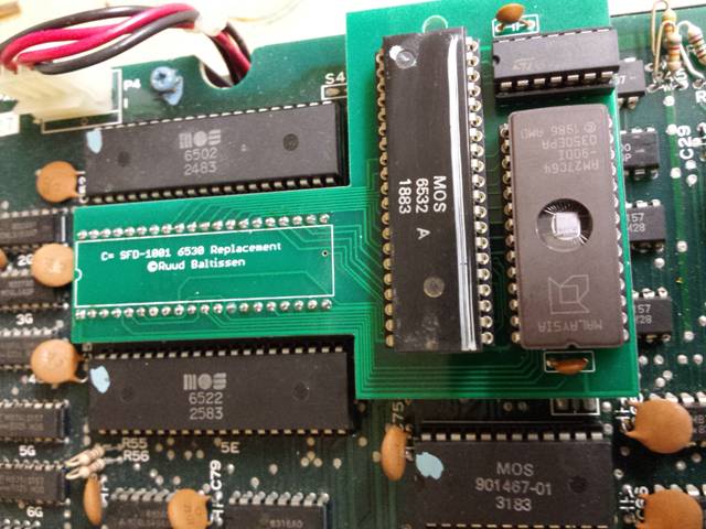
What is it?
Various IEEE dual floppy drive have a 6530 on board. This is a masked programmed IC, for details read this document first. There is only one problem with this IC: if it breaks down, new ones aren’t available anymore and second handed ones are rare. Good reasons to develop a replacement.
Attention: Commodore produced various 6530s, for example the ones used in the KIM-1. This design cannot be used to replace these ones, it is only meant to replace the 6530 in the following drives:
– 2040
– 3040
– 4040
– 8050
– 8250
– 8250-LP
– SFD-1001
First some credits
My (Ruud Baltissen) prototype did not work so I asked the CBM-Hackers for help. Gerrit Heitsch, Gordon Steemson and Martin Hoffmann-Vetter both pointed me to some critical errors in the design. Thank you very much!
The design
The main reason for developing a 6530 replacement was running out of 6530 spares. Unfortunately it wasn’t as simple as with building the KIM-1 replica.
The 6530 can be divided in three parts:
– the ROM
– the RAM
– the I/O
The design: the ROM
One of the great helps here was this schematic found at www.zimmmers.net. For selecting the ROM, the input /RS0 must be set to (L) and the input /CS2 must be set to (H). So I used /RS0 in the first place to enable the EPROM on my PCB by tying these inputs directly to /RS0.
I noticed that the 8250LP and SFD-1001 have a little PCB on the place of the 6530. On this PCB you will find a 6530, an EPROM and a 74LS04. The reason for this PCB was that Commodore needed to update the ROM for one or another reason. And probably it was cheaper to create this PCB than producing new 6530’s.
Anyway, the CS input of the EPROM has been connected to /RS0 of the original socket. The /RS0 input of the original 6530 has been connected to +5V. This only confirmed that my idea how /RS0 should be used was correct.
One gate of the 74LS14 is used to invert PHI2 and the result is used to control the OE input of the EPROM. This construction is needed because there are two 6502s on the main board. Each 6502 has its own address bus but both 6502s share the same data bus. This is made possible because the second 6502 runs on the inverted clock of the first one. The inverted PHI2 on the OE input makes sure that the EPROM only outputs its data when the right 6502 is in command.
The design: the mapping of the RAM and the I/O
If you have another look at the schematic you will see that both the 6532 and the 6522 share the same Chip Select line coming from output 0 of the on board 74LS42. My first impression: quite confussing!
Most helpfull after all appeared to be the disassembly I made of the disk controller of the 8250. The memory map for the disk part looks like this:
$0000 – $0029 : 6530 RAM
$0040 – $004D : 6522 registers
$0080 – $008F : 6530 registers
$0100 – $01FF : possible stack
We know the 6530 has 64 bytes of memory on board so we can assume:
$0000 – $003F : 6530 RAM
The input /RS of the 6532 tells it when to select RAM or I/O. Connecting it to A7 makes sure that the RAM and the I/O of the 6532 fit in the above table.
The I/O and memory of the 6530 are mapped to the first KB, $0000 – $0400. Having found no further decoding, it means everything should be mirrored every 256 bytes. So the memory mapped to $0000 – $0040 should also appeare at $0100 – $013F. And this is confirmed by the source code: the Stack pointer is set at $3F.
Then what about the 6522? Here we run into a very strange thing: as said before, the 6522 shares the Chip Select line for its negative /CS input with the 6530. The 6522’s positive CS input is connected to address line A6. This means that the 6522 is only active within the range $0040 – $007F, which is confirmed by the disassembly. Due to mirroring it is active within $00C0 – $00FF as well. And further it is also mirrored every 256 bytes within the first KB, just like the 6530.
And now the puzzling thing: when the range $0040 – $007F (read: 6522) is selected, the 6530 is selected as well and yet there is no conflict. Conclusion: a circuit inside the 6530 takes care of not selecting the 6530 for this range.
So we must take care that the 6532 is not selected when the 6522 is. This is realized by inverting A6 and connecting the result to the CS1 input of the 6532.
The design: the I/O
The internal mapping I/O of the 6532 is not the same as the mapping of the I/O of the 6530. For exact details, please see the page about the KIM-1 clones. To make things work the original idea was to invert address line A4 towards the 6532. Although this will work under normal circumstances, it won’t the moment a program addresses a mirror address. The OR gates IC4c and IC4d take care of that.
Maybe you noticed the connection between PB7 and IRQ, I read about that construction in some documents I received with my KIM. I haven’t any idea if this is present in the 6530 for drives. So far I my drives functions fine with it.
The schematic

I think the only explanation that is needed is about the wiring of the EPROM. All unneeded wires are wired to +5V. This enables you to use any EPROM from 2716 to 27512. The original file you will need is only 1 KB. You have to program it in top 1 KB of the EPROM. If using a 2764 it must be programmed in $1C000/$1FFFF. You will find the binary here.
Attention: the ROM of the SFD-1001 is 2 KB, you should only use the first 1 KB. Check this with a tool! (for example: DEBUG under DOS)
The Eagle schematics as ZIP file.