Focal on the 6502, a page on this small language, originating for Digital Equipment.
A small interpreter (about 5K) for a convenient interpreted language. Floating point 9 digit accuracy. At least two versions were distributed around 1977, one by Aresco, called “Focal V3D” and another by the Program Exchange as representative of the Denver 6502 Group, “Focal-65″ or FCl_65” or “FCL-65E”
Information from the German 1981 article in MC Magazine, see the articles, indicates the existence and sale of Focal versions by the 6502 Program Exchange:
- FCL-65 and FCL-65E with Mini userguide
- My version from Aresco Focal V3D, 1-oct-1977 binary and userguide
- Focal V3D for TIM, listing known and available on this page
- Focal-65 V3E 1-oct-1979, Apple II, source listing known at MC Magazine in 1981
- V4 for Apple, listing known and in possession of Wayne Wall, not public available
I suppose this list is incomplete, other versions may have existed. None but my binary of Aresco Focal-3D, the Aresco V3D Userguide, a User Guide by the Denver 6502 group and a listing of Focal-65 V3D for the TIM survived and is available.
Latest addition to this page is a reconstruction of the sources, of Focal V3D for the TIM to binary, and a port to the KIM-1. Also the Aresco version source is reconstructed and identical to the tape dump of 1978.
On this page you will find:
- My experience with Focal-65 as started in 1979
- Reference material: User manuals, listings
- Magazine articles about Focal-65
- Reconstructed sources of Focal-65 for TIM and KIM-1
- Reconstructed source of Focal-65 for the KIM-1 Aresco version
- On the origin of Focal-65
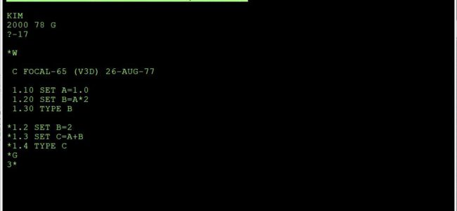
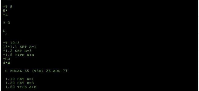
My experience with Focal-65 started in 1979
In 1979 my good friend Anton Muller, at a meeting of our Dutch 6502 KIM Club, surprised me with a package Anton had imported from the U.S.A. : Focal V3d by Aresco.
The package came with a cassette tape and a user manual. We installed it on the KIM-1 and played with it. Impressive what was done in about 5K!
Floating point, string handling, a trick to suppress the hardware echo of TTY input.
After an article in our club magazine more members of the club became Focal-65 users and published articles about it.
This version of Focal-65 has survived. I have dumped a working version from cassette in 2004 (not the original alas, but a working copy with a bit too much) and scanned the user manual.
Manual and binary version have been available on this website now several years. Also I added DEC Focal manuals, Digital Equipment Corp. developed and sold Focal as a product for the PDP computers. In the KIM/6502 User notes articles were published on making Focal even more interesting, also published here.
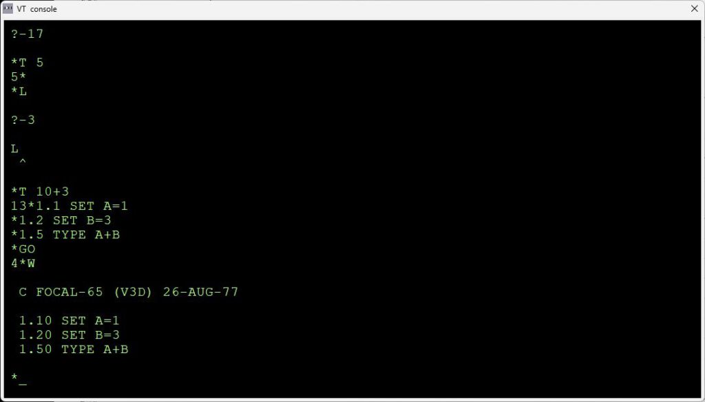
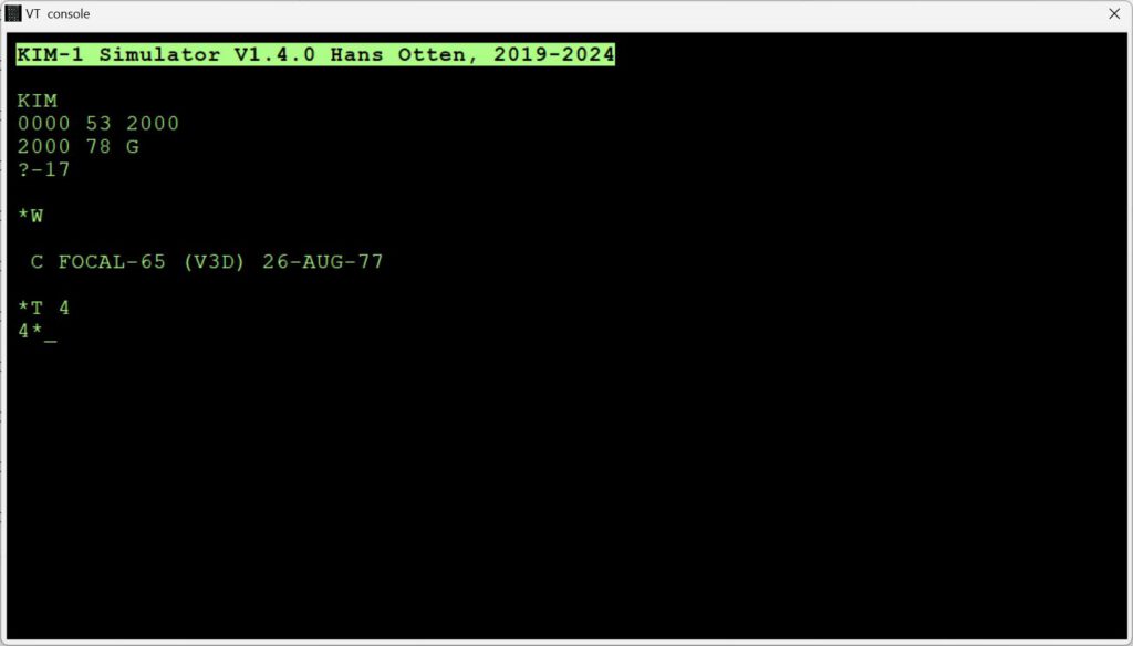
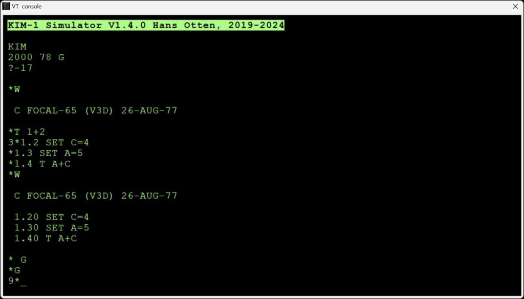
When the KIM Simulator became usable, I tested Focal and saw that suppressing the TTY echo worked, but the wait for keyboard input loop preceding the read character routine did not. So I added a setting to let Focal-65 survive that loop. So Focal-65, Aresco version, runs unaltered on the KIM-1 Simulator!
 |
The FOCAL programming language |
In 2023 a source listing appeared, thanks to Paul Birkel, of Focal-65, programmed by Wayne Wall and friends in 1977. Target system is a TIM such as Jolt or Superjolt. I typed in that listing exactly with modern assembler syntax and made that version operational.
Here I present several reconstructed versions, for TIM (653-004) such as Jolt and KIM-1 based systems.
– A TIM/Jolt/Superjolt system needs minimum 8K RAM in lower memory.
– The KIM-1 needs memory, minimum 8K, from $2000 and up.
See below for the TIM version and a port to KIM-1. These are 90% identical to the Focal-65 V3D Aresco version, so that was the start to recreate that source too .
Reference material for download
First some downloadable reference material.
Articles on Focal-65
KIM/6502 User notes
Articles from the magazine, Focal corner
- Introduction to FOCAL, 6502 User Notes 12
- Improve on echo problems with KIM TTY, 6502 User Notes 13
- Make room for enhancements, extend to 8K, User Notes 14
- Speed it up, 6502 User Notes 15
- Cassette save/write an LED display listing, 6502 User Notes 16
KIM Kenner
Introduction to FOCAL, how to program, Dutch
Compute II
Modify and Move FOCAL 65-E into EPROM, Compute II Issue 3
MC Magazine
German article on Focal-65, has interesting information on versions
Working versions, reconstructed from sources
Denver 6502 Group Focal for TIM
In 2023 a listing of Focal-65, by Wayne Wall, for a Focal-65 version for the TIM, showed up, thanks to Paul Birkel.
A low low quality scan, so I cleaned it up, improved contrast, removed artefacts and cropped it. The result is readable, but not fit for OCR.
I typed this source in, exactly as the listing: uppercase, same comments, same line numbers.In this way I honor the original author and also enable checking of the binary result.
I did change the assembler syntax to a modern assembler. The original was written for PAL-65, an assembler by Wayne Wall in PDP macro assembler format.
When it assembled I compared the binary out to the binary in the listing by hand. Of course typos and the curse of direct addressing, the #!, caused some extra work.
The result was a binary with the same length. as shown in the listing.
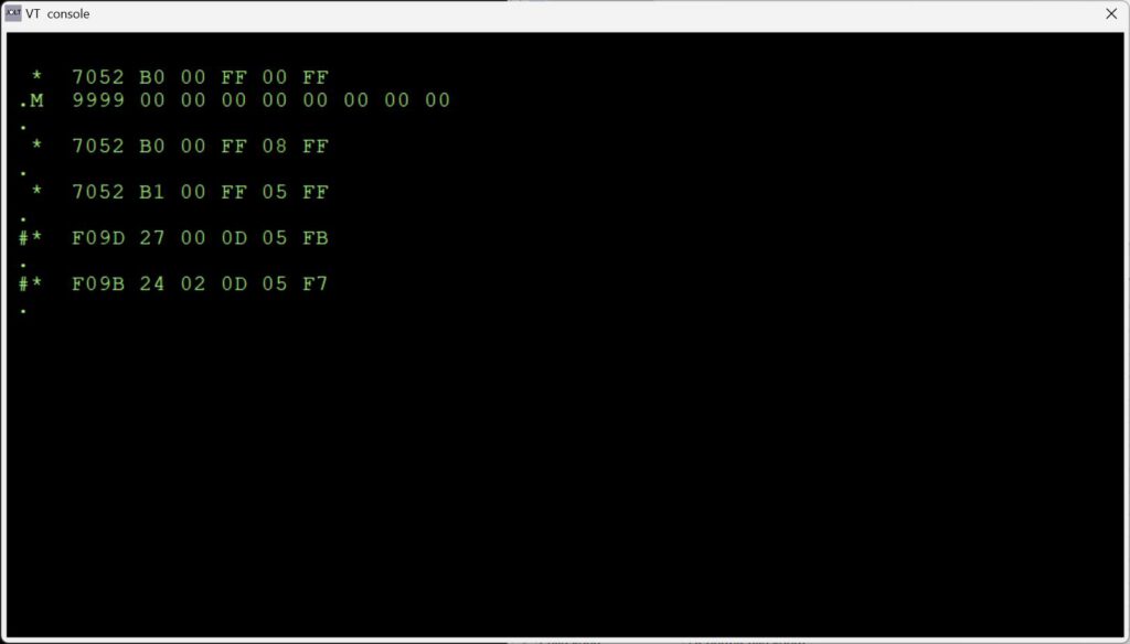
Then the binary was loaded in my TIM Simulator, with a small external patch for the ‘no echo’ input character routine in the source. The TIM has ‘software echo’ hardcoded in the monitor for reading a character from TTY, so the monitor code is copied with optional echo.
It runs!
Focal-65 for the TIM, here the source as typed in, listing, binaries in Intel hex and Papertape format and the TIM Simulator patch.
Denver 6502 Group Focal for the KIM-1
To illustrate how easy it is to adapt Focal to other 6502 systems, I ported the TIM version to the KIM-1.
Changes required:
- Program moved from $1000 to $2000
- Replaced the TIM I/O package with a KIM-1 version: IRQ/BRK vector, no echo character input (partly taken from the Aresco disassembly for character output
- Further no changes, same line numbers, same size
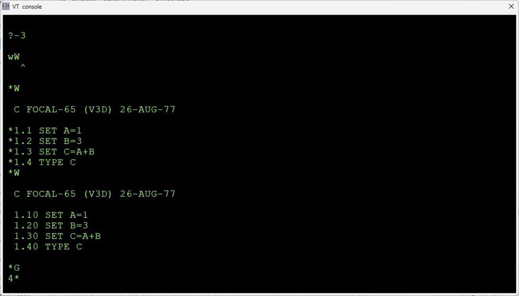
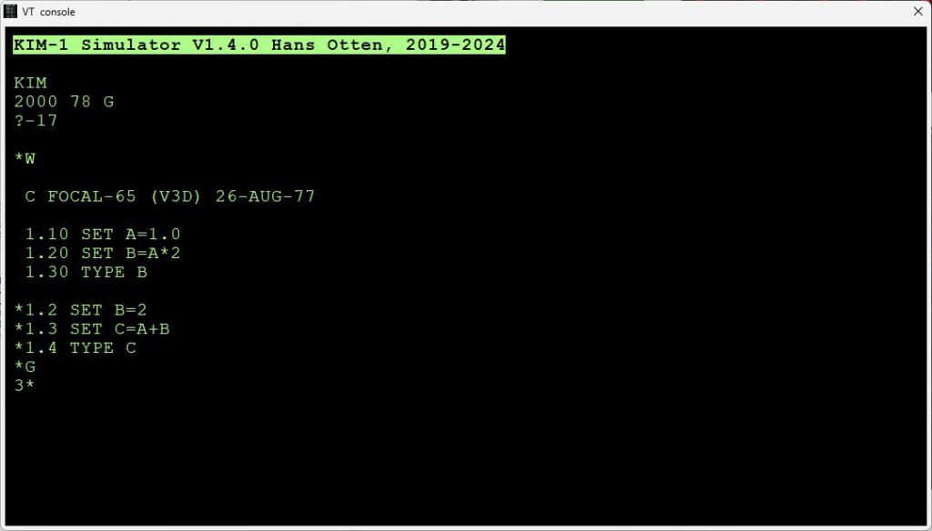
This version runs fine in the KIM-1 Simulator with the Focal V3D setting.
Focal-65 for the KIM-1, here the source as typed in, ported to KIM-1, listing, binaries in Intel hex and Papertape format
Aresco Focal-65 V3D
Here the original Aresco Focal V3D dump from cassette. Note that the dump contains a bit more than necessary. The zeropage is completely dumped, and filled in by a running Focal session.
It runs on a KIM-1 and on the KIM-1 Simulator with the Settings – Type of Break setting set to Focal V3D.
First attempt to get a source, unfinished, does not assemble, but informative.
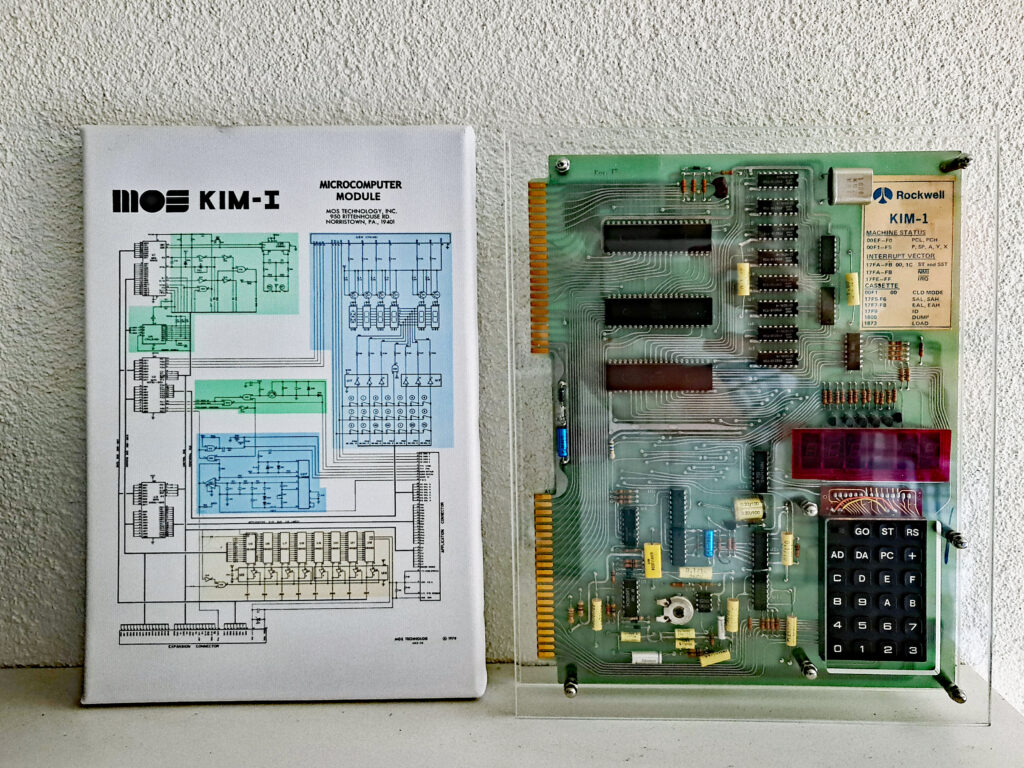
Disassembled source by Paul R. Santa-Maria (2004) and Hans Otten (more comments) (2022).
Reconstructed source of Focal-65 for the KIM-1 Aresco version
With the source of the KIM-1/TIM and the binary of the Aresco version I have since 1978, it was an easy job to reconstruct the source of the Aresco version.
By comparing the binary output of the assembled source and the binary of the tape, differences can be seen and fixed in the source.
The interpreter code is 100% identical to the tape dump (minus the extra unused bytes saved at the end). Zero page is clean.
The code runs in the KIM-1 Simulator with the Focal V3D setting. No surprise, the binary of the tape dump also runs and the binaries of the code are identical.
Focal-65 for the KIM-1, Aresco version, here the source , listing, binaries in Intel hex and Papertape
The history of Focal for the 6502
Excerpt from the history of the Denver 6502 Group.
In 1975, Denver was a hotbed of computer activities. There was a new computer club called the Denver Amateur Computer Society (DACS), and every meeting was packed with radio amateurs and hobbyists anxious to learn about this exciting new technology. DACS was dominated by Intel 8080 based computers, but there were a few people interested in the 6502. Wayne Wall was one of the first to appreciate the power and speed of the 6502, and he decided to form a subgroup of DACS for 6502 users.
Wayne was a genius assembly language and systems programmer who worked at the Colorado School of Mines. He began holding meetings every Tuesday night at the School of Mines Computing Center for anyone interested in the 6502. At first it was called the 6502 sub-group of DACS, but as time went on, it became the 6502 Group.
All told, there were probably about 100 members, but on a typical night, 30 to 40 people would crowd into the meeting room, anxious to hear Wayne’s latest ideas and see his demonstrations. He was famous for his magic shows that invariably consisted of doing something hitherto unimaginable like simulating human speech with 13 bytes of assembly code. Wayne quickly gained the well deserved reputation as a computer wizard.
Most members of the group owned Digital Group systems. The Digital Group was a local company that had a short but spectacular career manufacturing computer kits. They were powerful, easy to assemble and way ahead of their time, with memory-addressable video cards, system monitors and relatively large memory boards. In addition to the Digital Group systems, the group had a scattering of Kim’s, Tim’s, Jolt’s and even a few odd homebrew machines.
At the time, there was virtually no software available for the 6502. All programs had to be tediously hand-assembled and typed into the machines. Wayne decided that his first task was to find a way to deal with this problem.
The School of Mines had a huge black mainframe called a PDP-10, and Wayne wanted to use the power and capabilities of this computer to write 6502 code. The first possibility was to use a FORTAN cross-assembler that was available from MOS Technology, but it was slow and buggy. Instead, Wayne chose to write 6502 macros for the PDP-10’s “PAL” assembler. After a few days work, Wayne had a fast new assembler that he called “PAL-65.” Suddenly we had the ability to write relatively large assembly language programs for the 6502.
Initially, Wayne cranked out a series of assembly language games. The first was a simple text based game where you shot arrows at a mythical beast called a Wumpus. Most of our computers had between 512 and two kilobytes of memory, but as Wayne’s games grew in complexity, we struggled to keep up, spending our nights soldering memory chips onto circuit boards.
Wayne now turned his attention to a high level language. The Intel based microprocessors had a version of BASIC written by Microsoft. Wayne decided that we should have a similar language, and he chose to write a version of the DEC language called FOCAL. Even though it was a relatively obscure language, FOCAL had some subtle advantages over BASIC, the biggest was its ability to evaluate strings as expressions.
Wayne wanted FOCAL to be a group project, and one evening he showed up with a stack of photocopies of the DEC flowcharts for the language. His plan was to assign each section of the chart to one of the 6502 Group members. We were supposed to go home, write 6502 assembly code for the section, and in a few weeks, we’d have an operating version of FOCAL. Unfortunately, Wayne had overestimated our skills. Most of us had been assembling code by hand and had no idea how to work from a flow chart. In the end, Wayne and Bob Ulshafer did most of the coding.
When it was finally finished, FOCAL was a big breakthrough. Suddenly we had a true programming language. Complex new games began to appear on our computers including a version of the famous mainframe game Star Trek, written by Larry Fish. Over the next few weeks Wayne wrote a five-byte floating point package for FOCAL based on a Dr. Dobbs article. With the new floating point power, simulations and mathematical programs sprouted up everywhere.
With thanks to Paul Birkel for the scan of the listing.

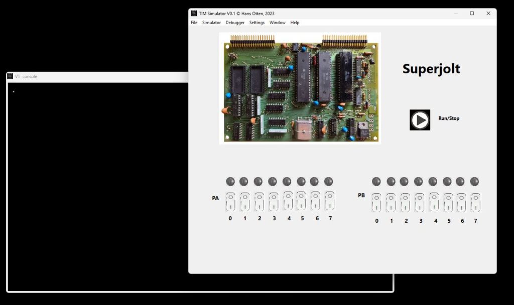
 TIM Superjolt Simulator V0.4, Tiny Basic working!
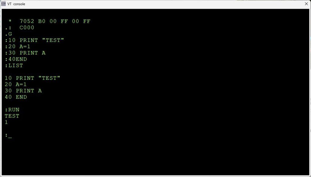
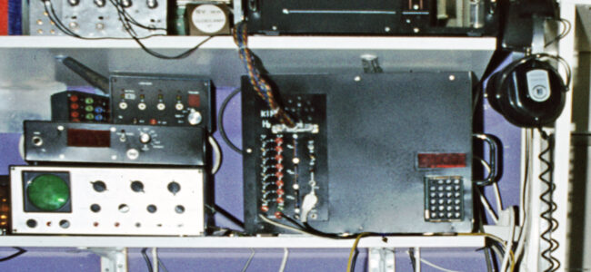
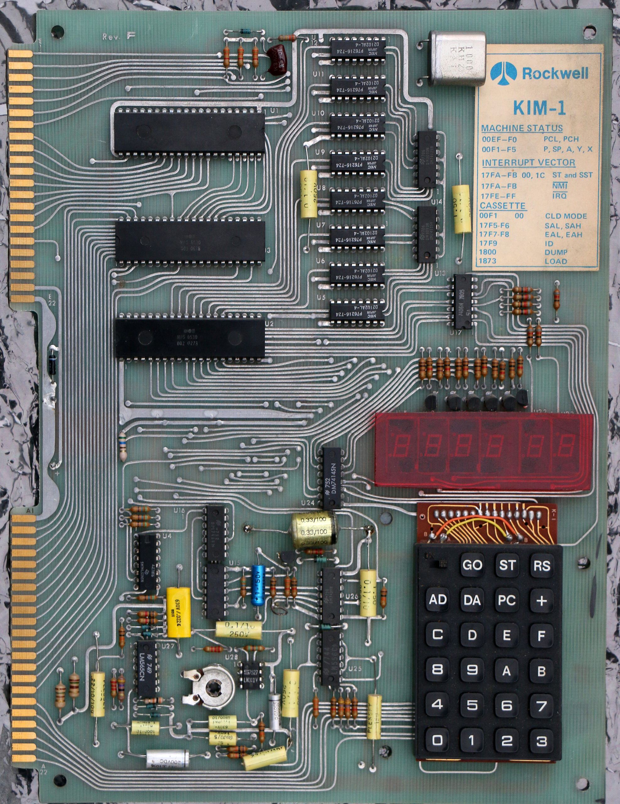
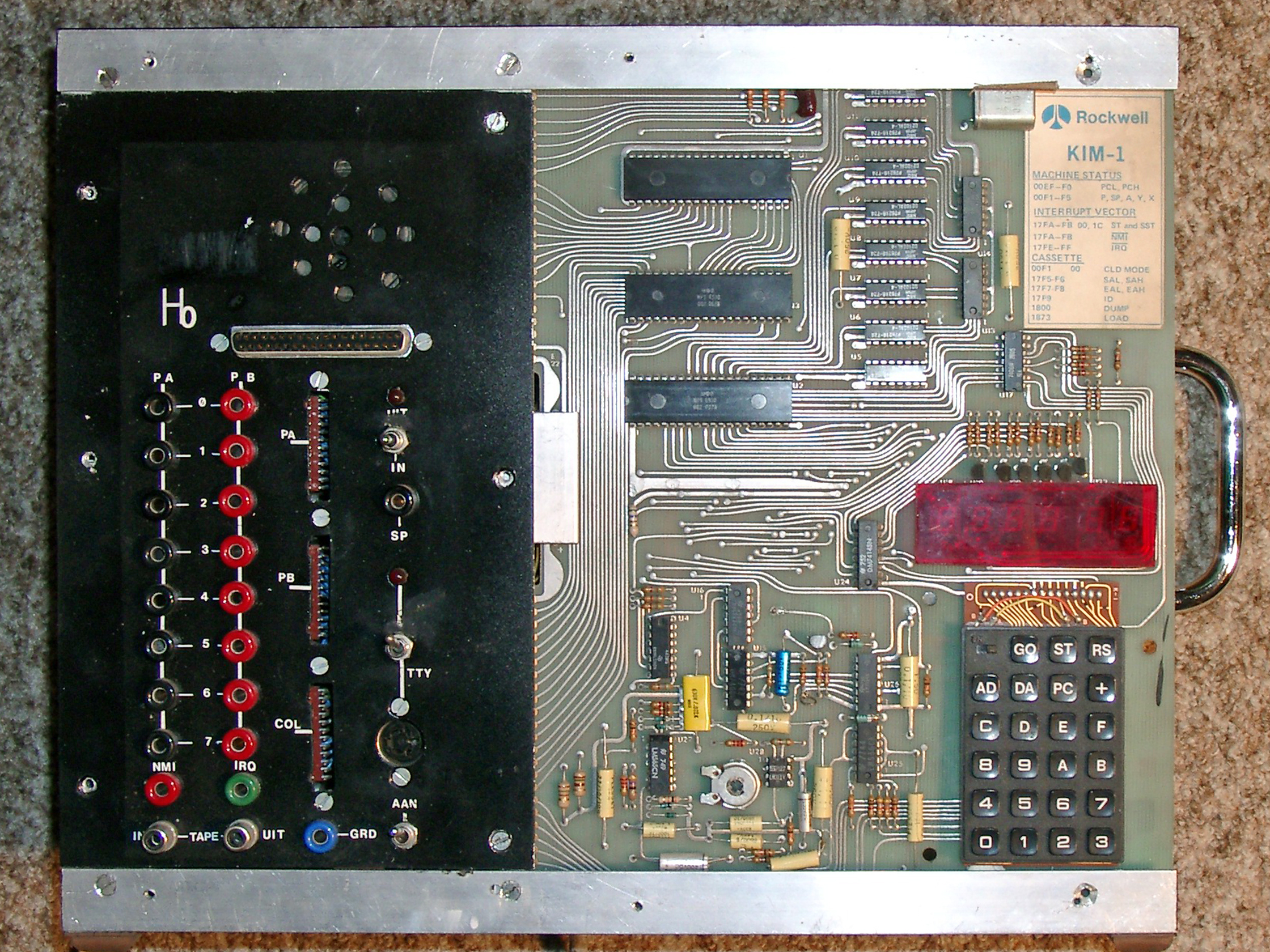
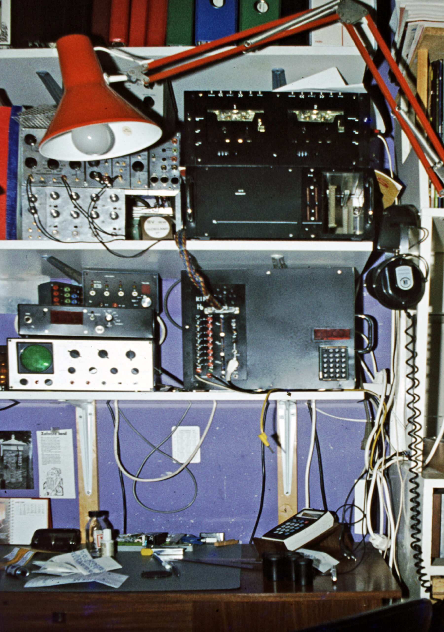
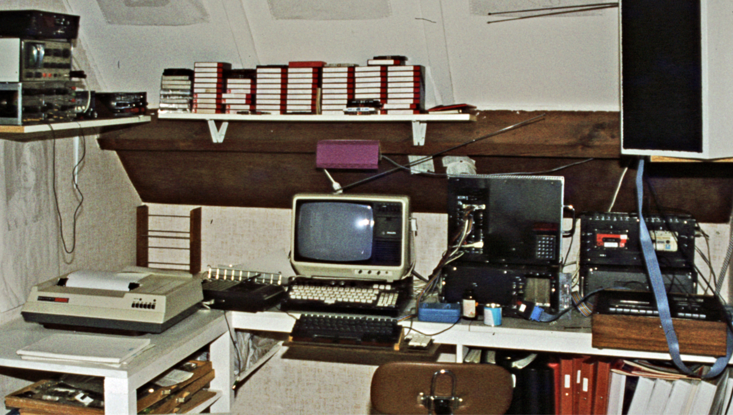
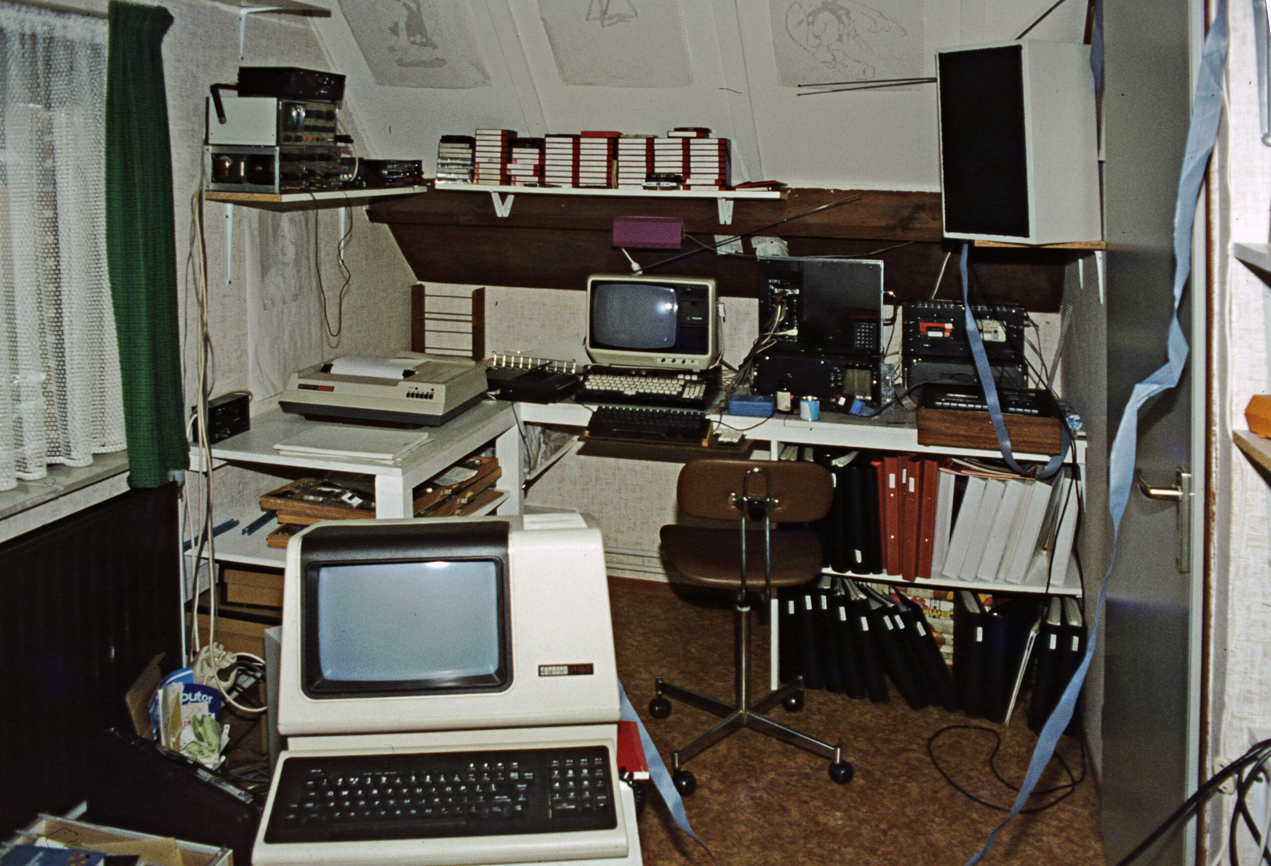
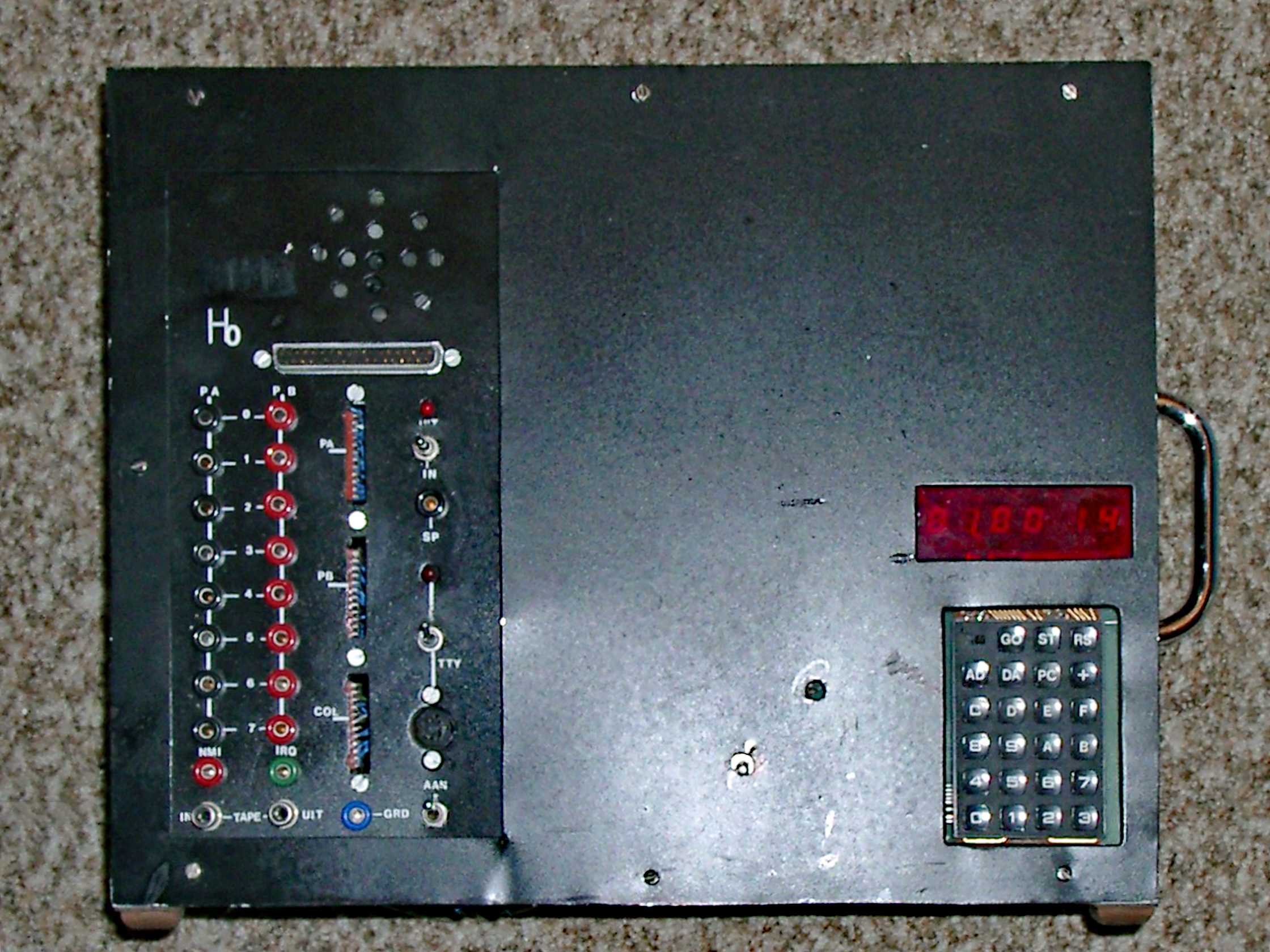
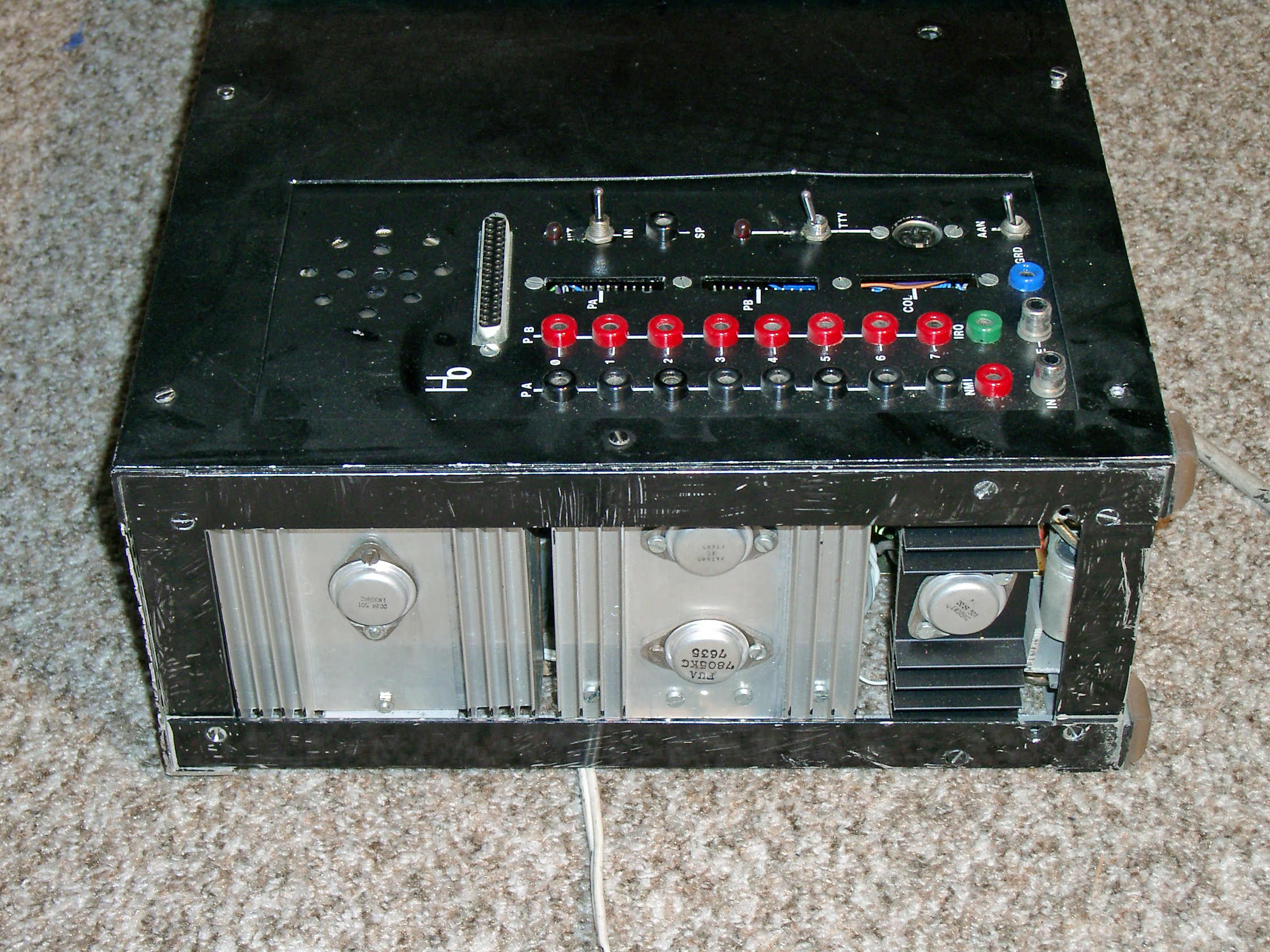
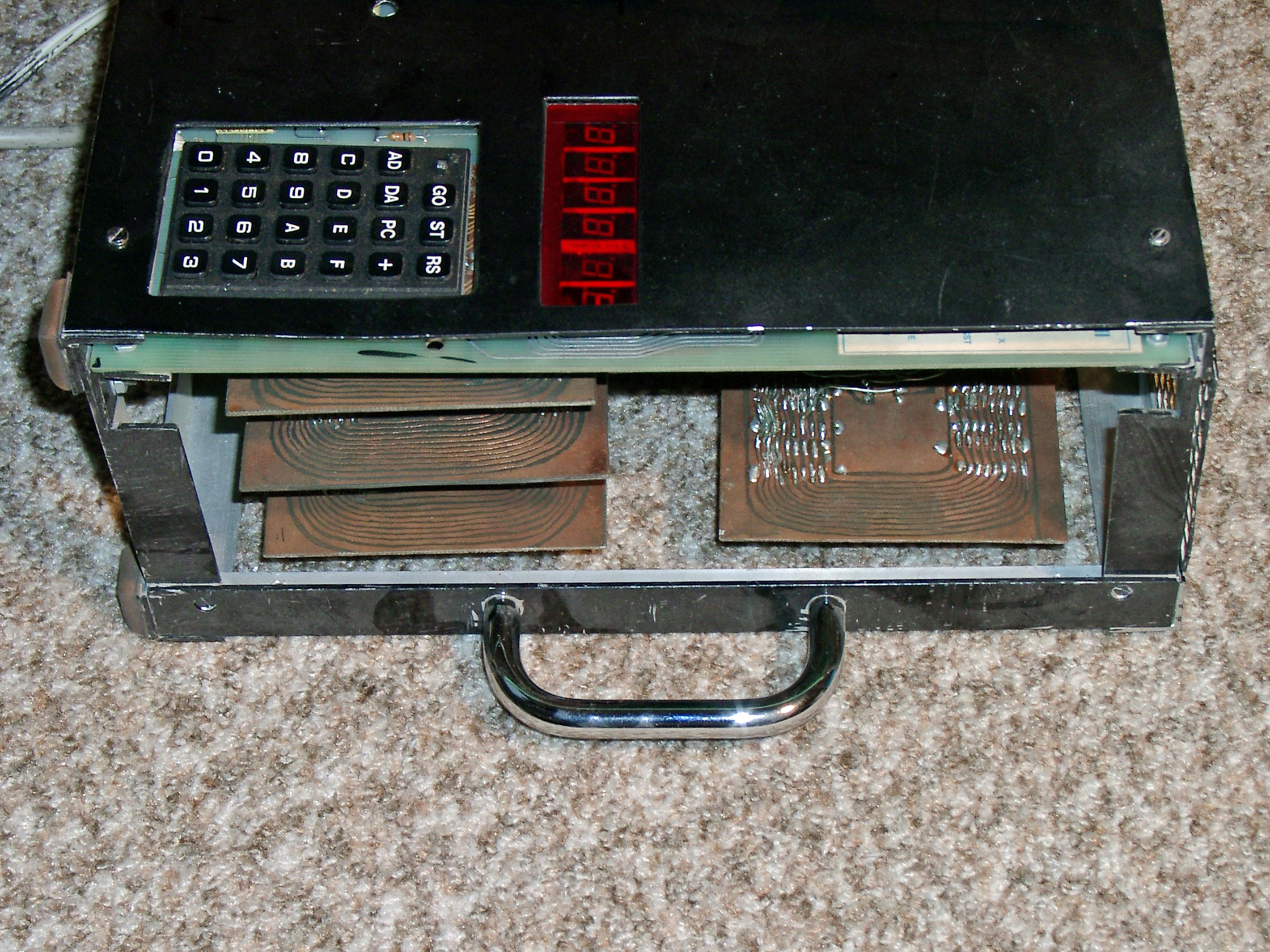
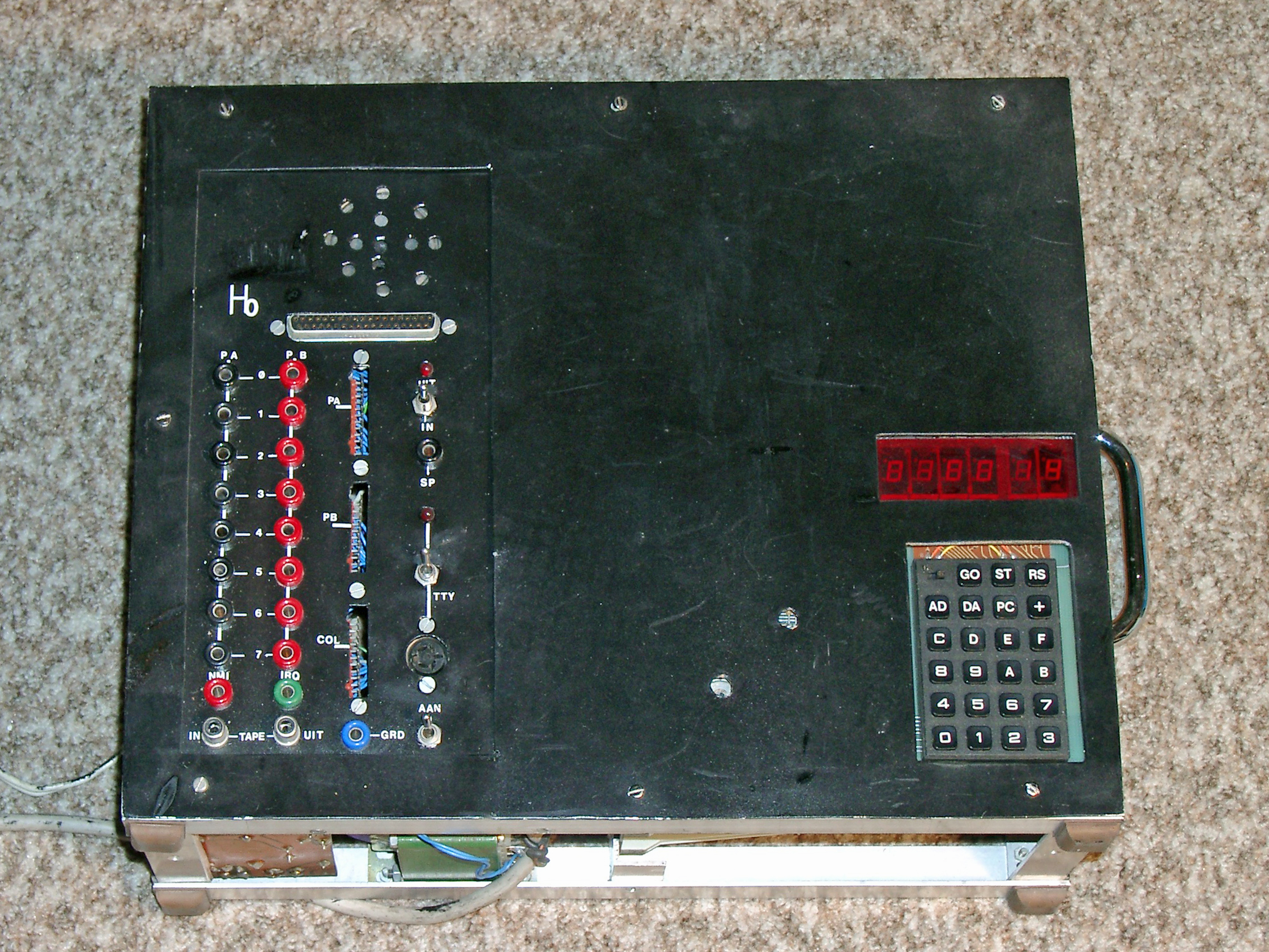
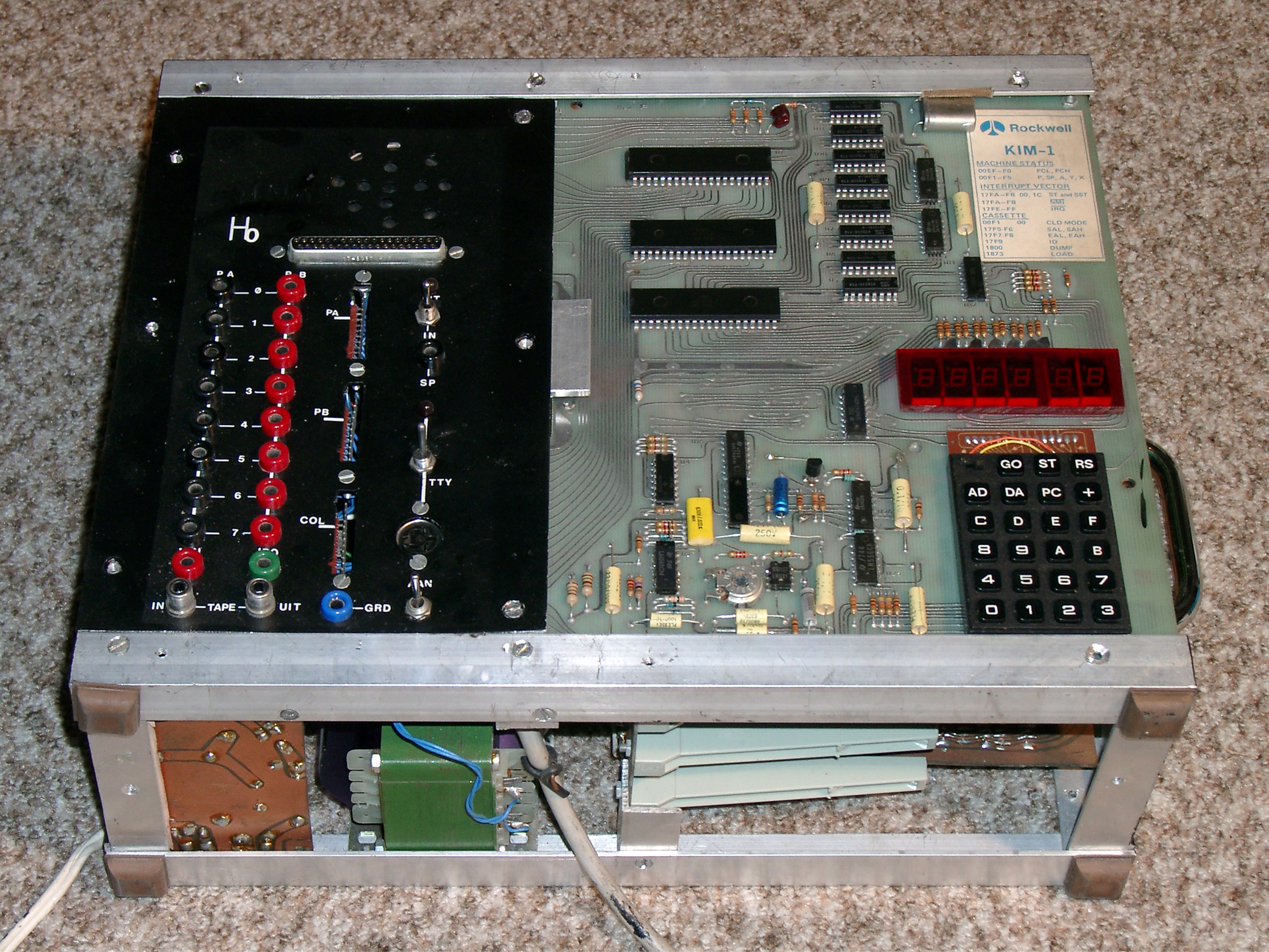
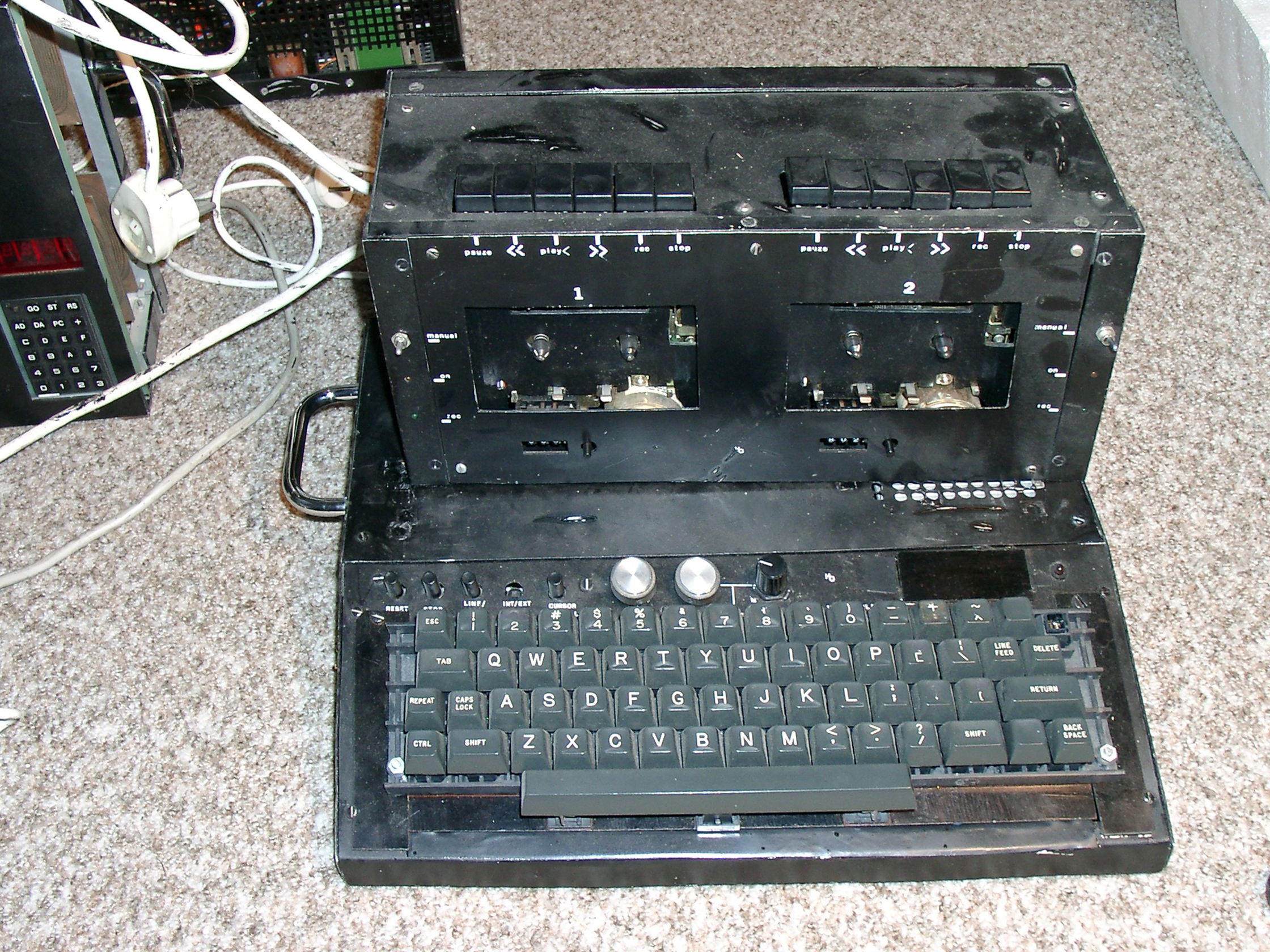
 First the KIM-1, I still have it, in working condition, in my private museum. Changes still visible, a red acryl cover over the LED displays, a capacitor moved to the back to make it flat enough to fit the case I made and some supports to have it lay stable and safe on a table.
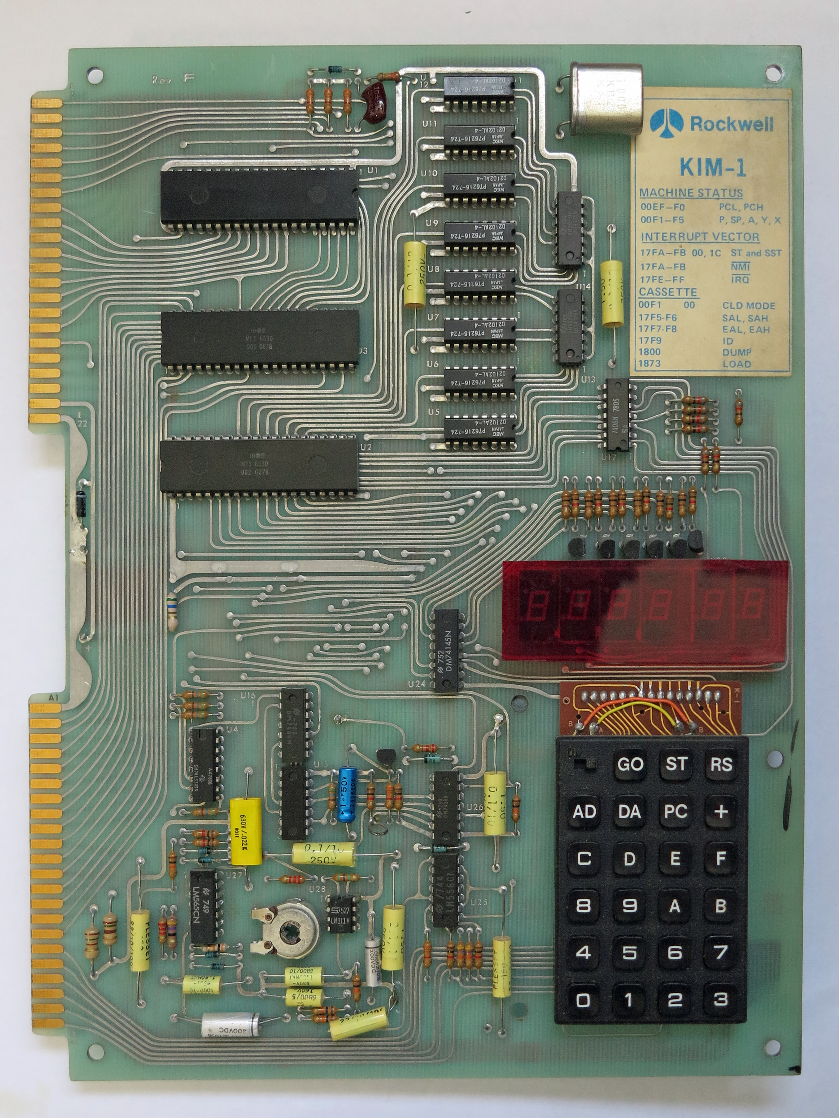


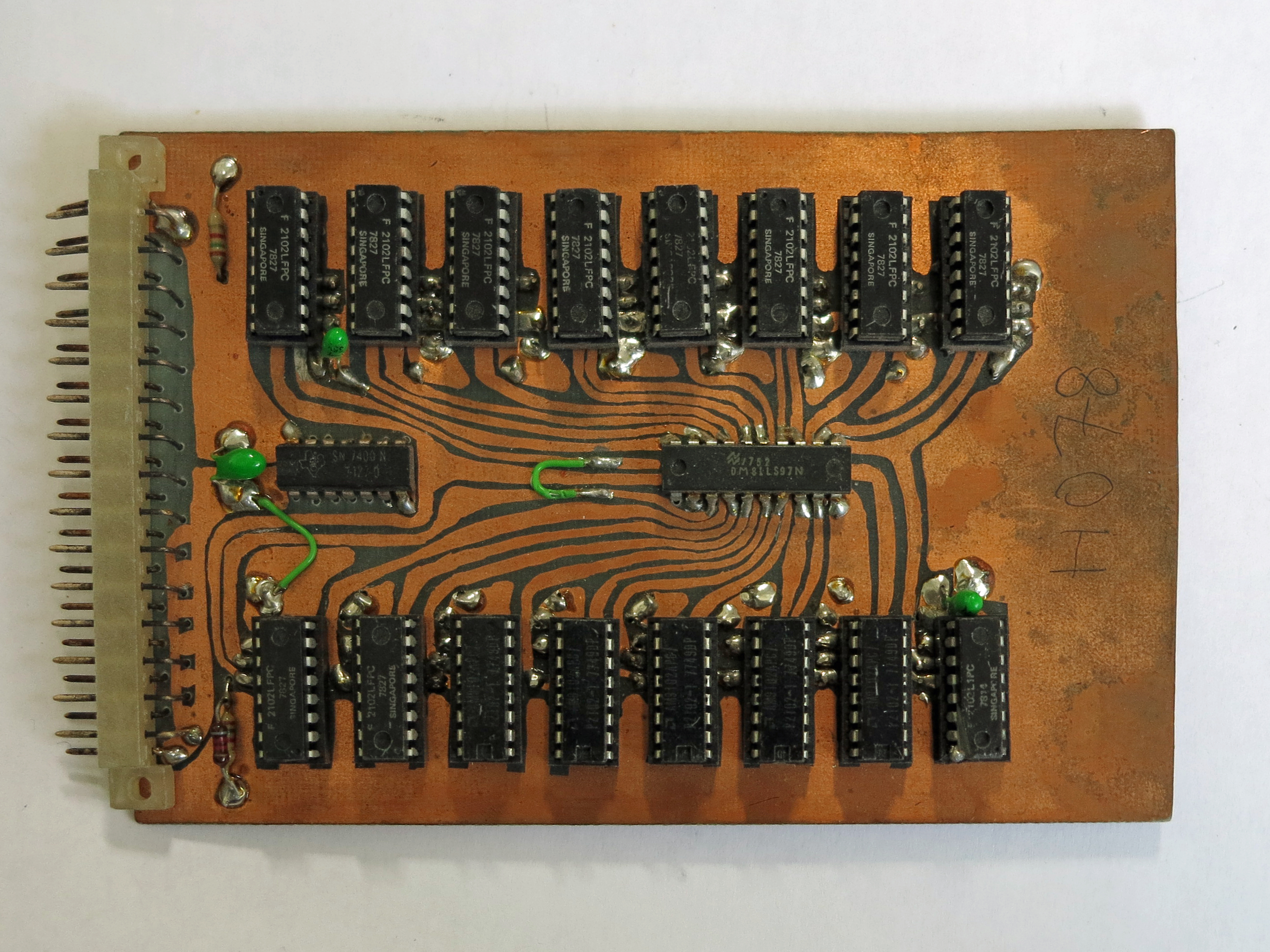
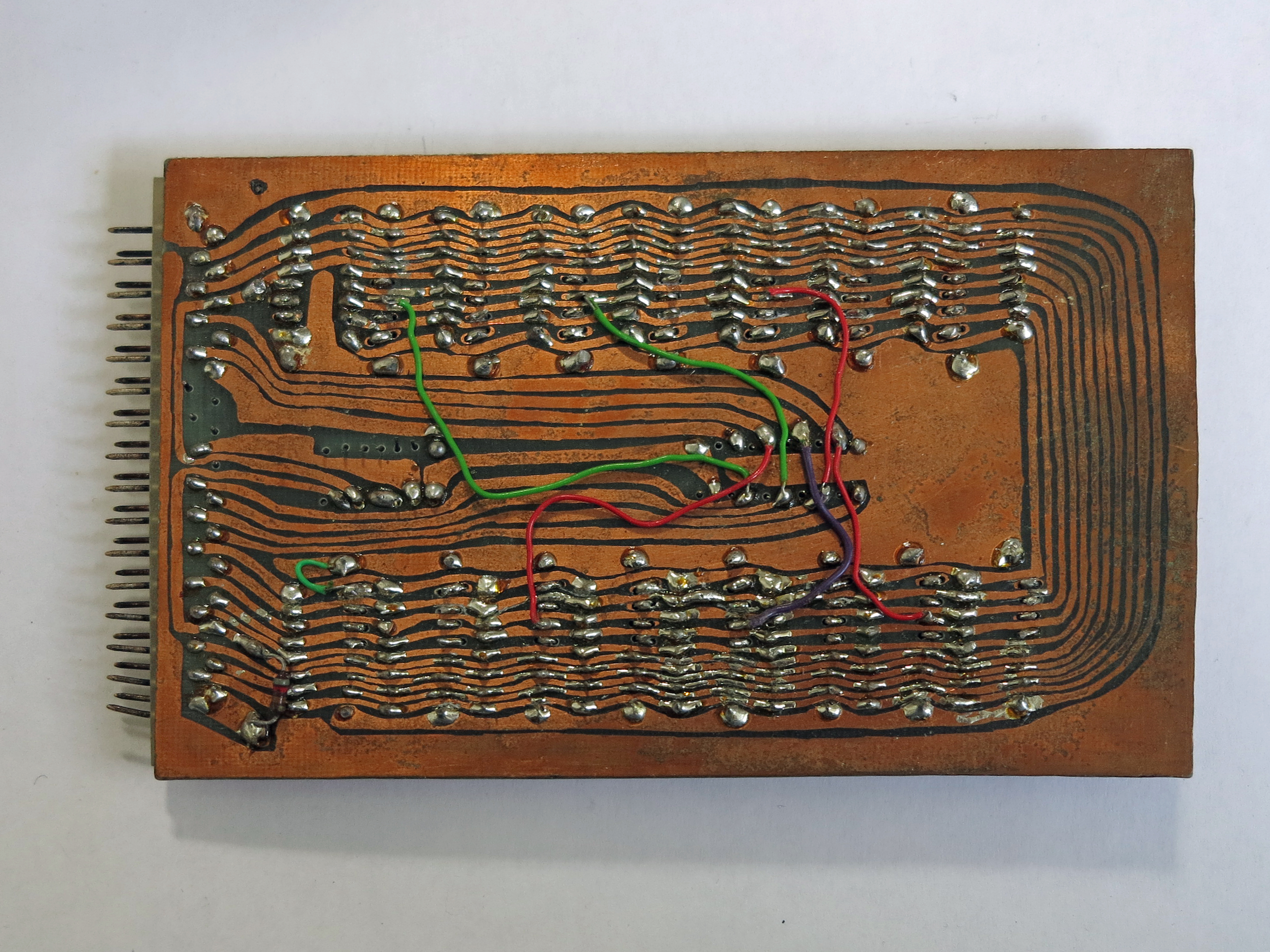
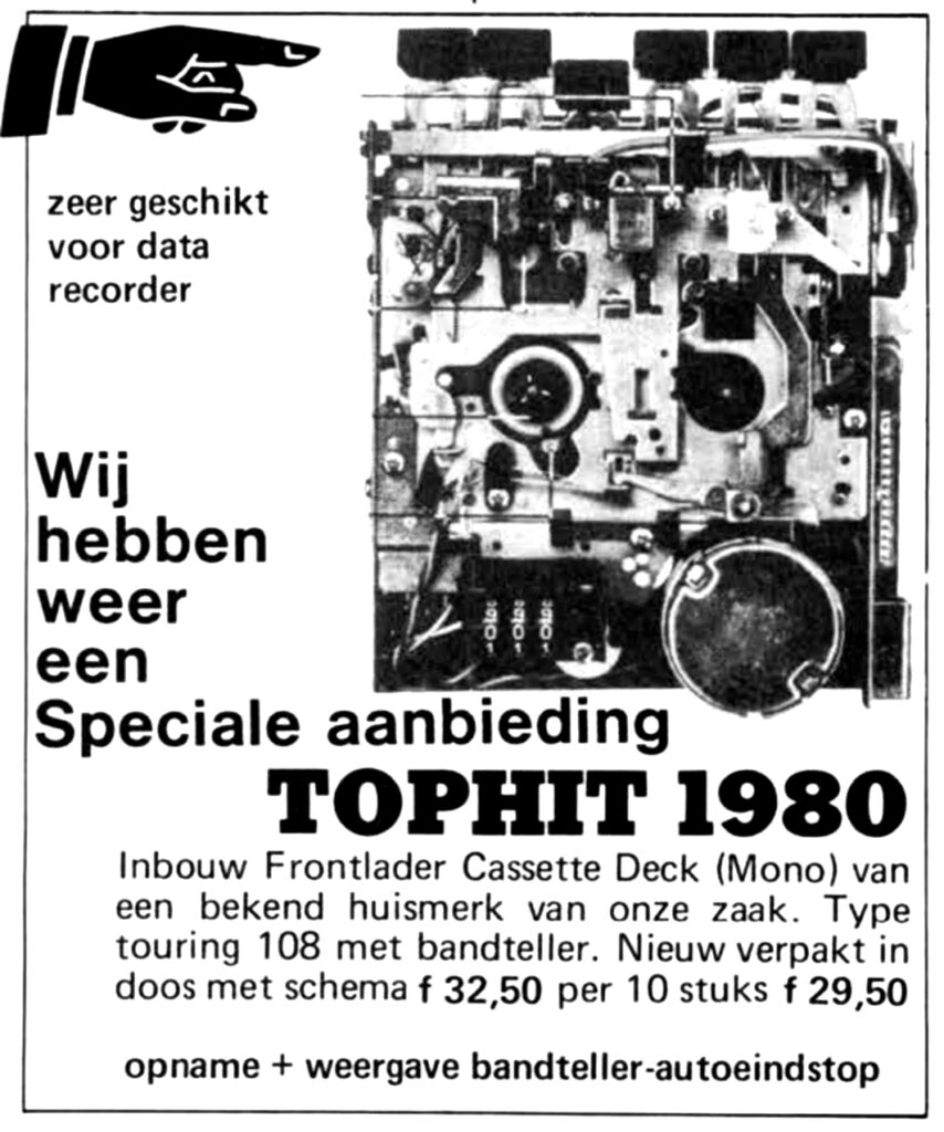

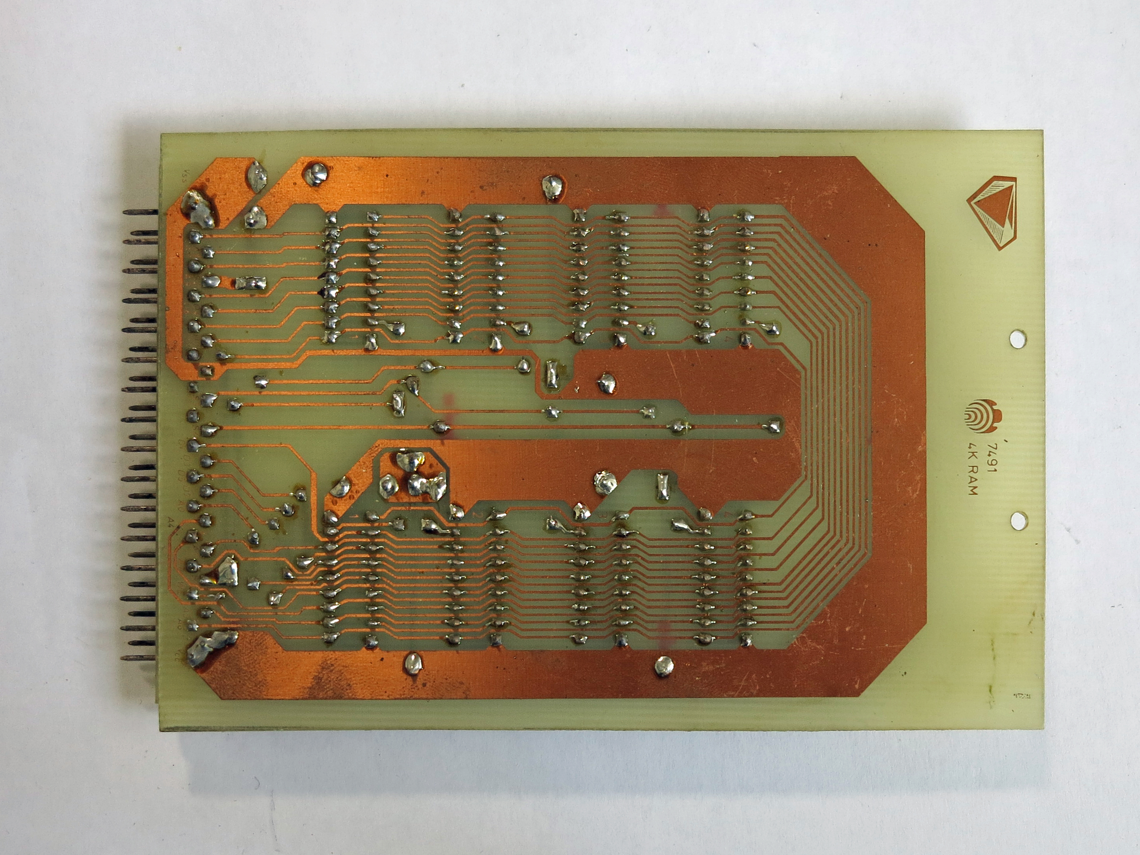
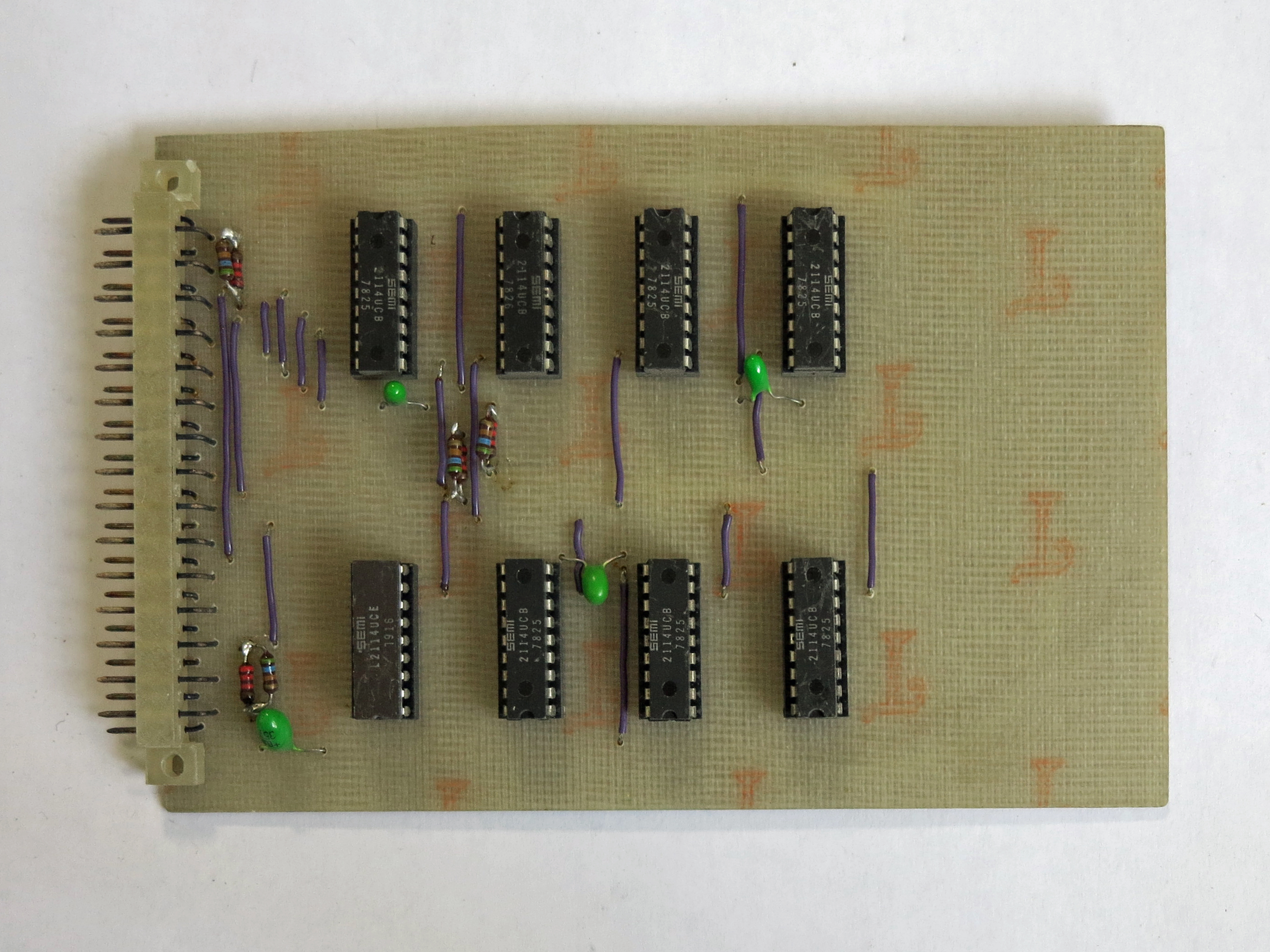
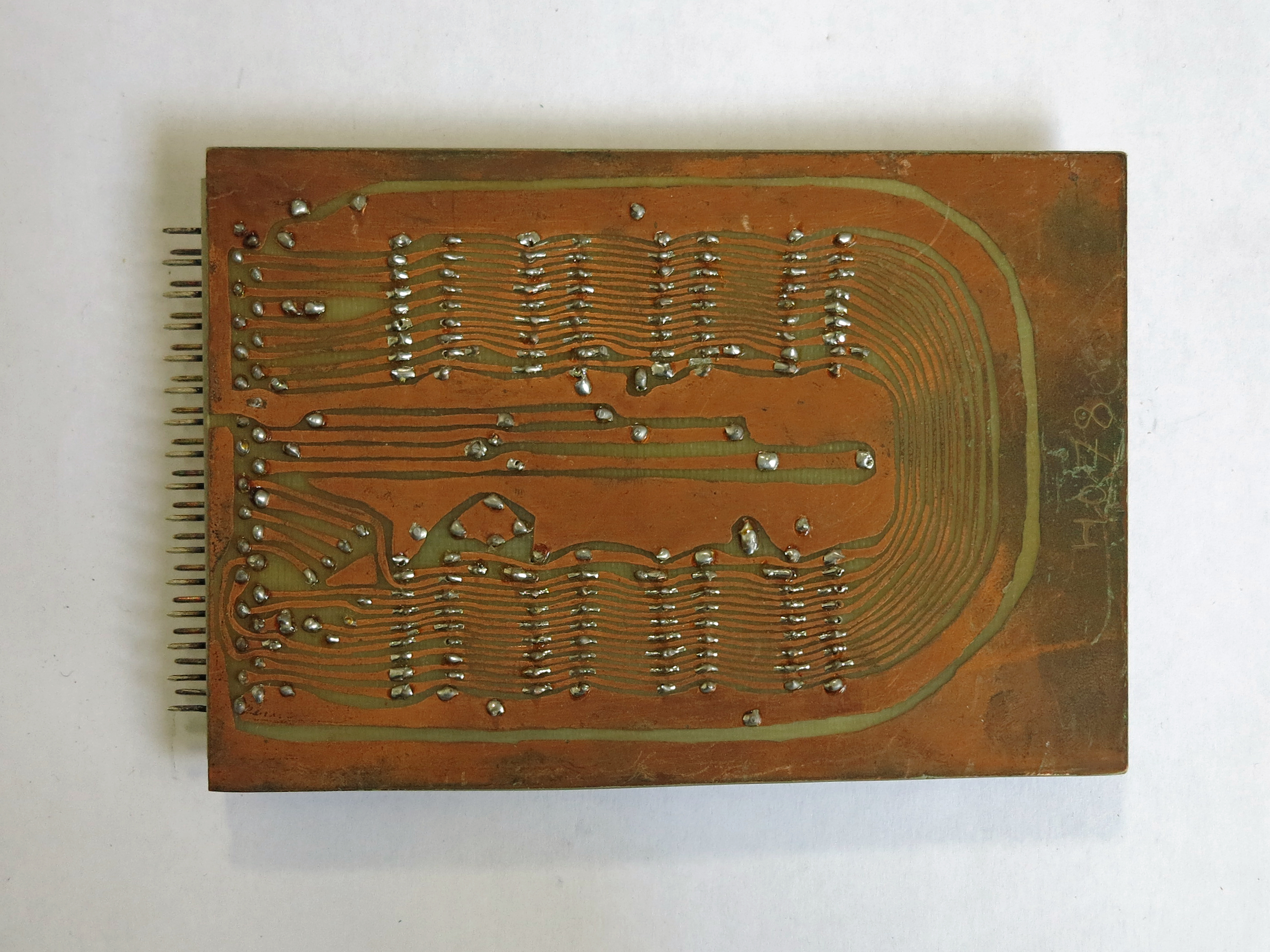
 4K SRAM card, Radio Bulletin September 1979