Bob Applegate used github repositories to archive and supplement some of his projects.
While this github archive is still up (August 2024), it may go away too.
So here dumps of the repositories. Some of the contents may also show up in the Corsham projects archive pages.
6502 Tiny BASIC
# 6502 Tiny BASIC
This is Bob Applegate’s (bob@corshamtech.com) spin of a Tiny BASIC interpreter for the 6502. It uses an IL approach, like proposed by Dr Dobb’s Journal in the first few issues. This is not fancy, it’s not bug free, and it’s not amazing by any means, but it was fun to write and decent enough to do fun stuff and run demos.
CTMon65
CTMon65 – 6502 monitor
Eagle Libraries
These are libraries used in Corsham Technologies LLC prodcuts (www.corshamtech.com).
# SS-50.lbr
This is for constructing SS-50 and SS-30 compatible boards. It includes both male and female Molex connectors. For constructing plug-in boards using a female connector my suggestion is to place the center of the library part 0.15″ above the bottom of the board.
# S-100.lbr
This is for constructing S-100 boards and is, for now, more of an experimental library rather than something that has any sort of polish about it. Feel free to use but don’t be too disappointed when it does not meet your expectations.
Kicad SS50
# KiCad SS-50 Library from Corsham Technologies, LLC
This is a free to use library that was developed during our creation of
various SS-30/SS-50 boards.
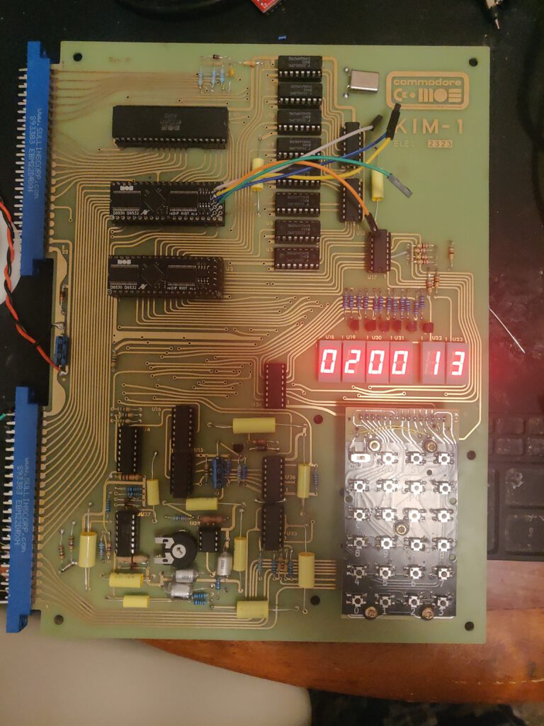
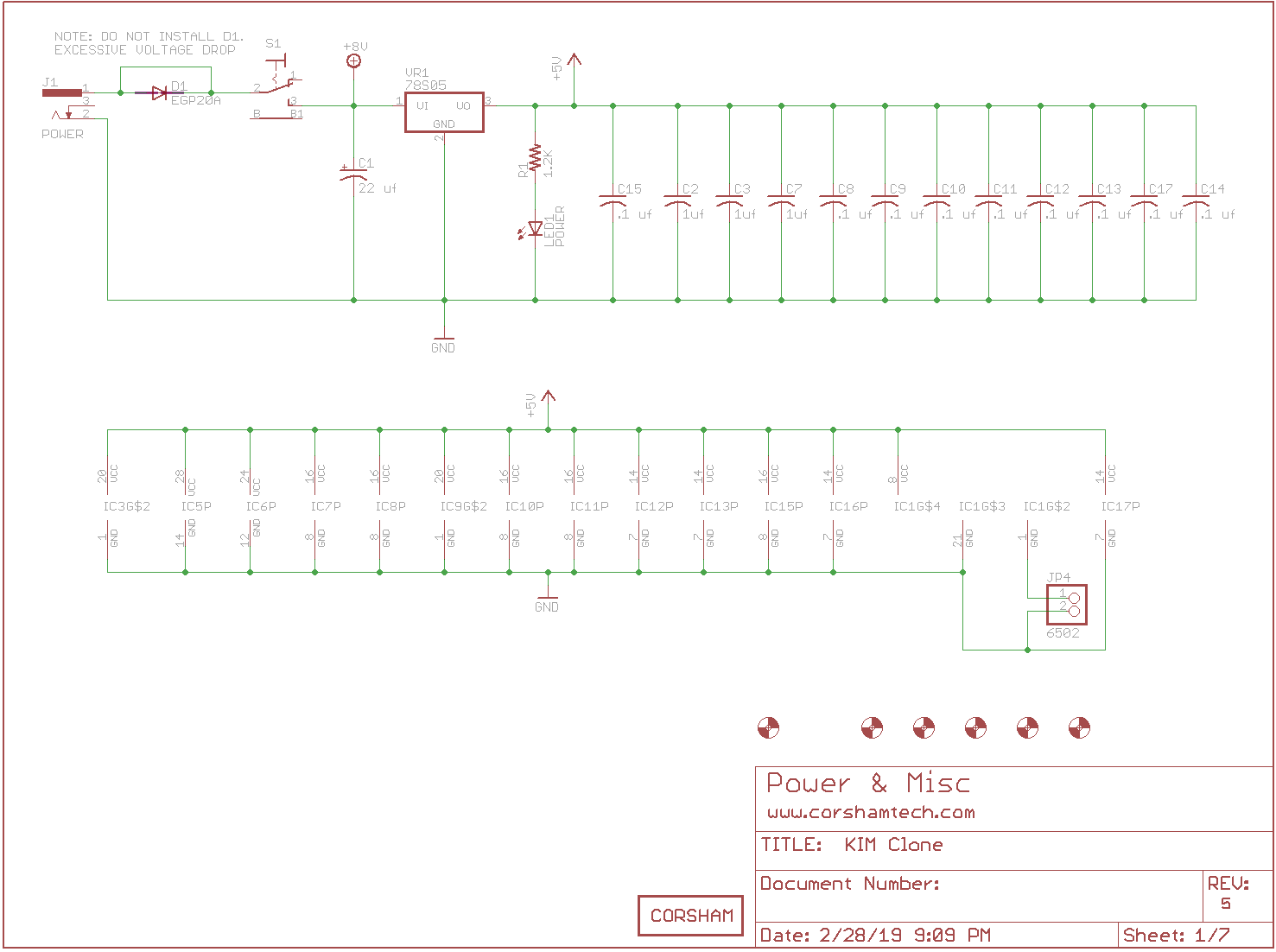
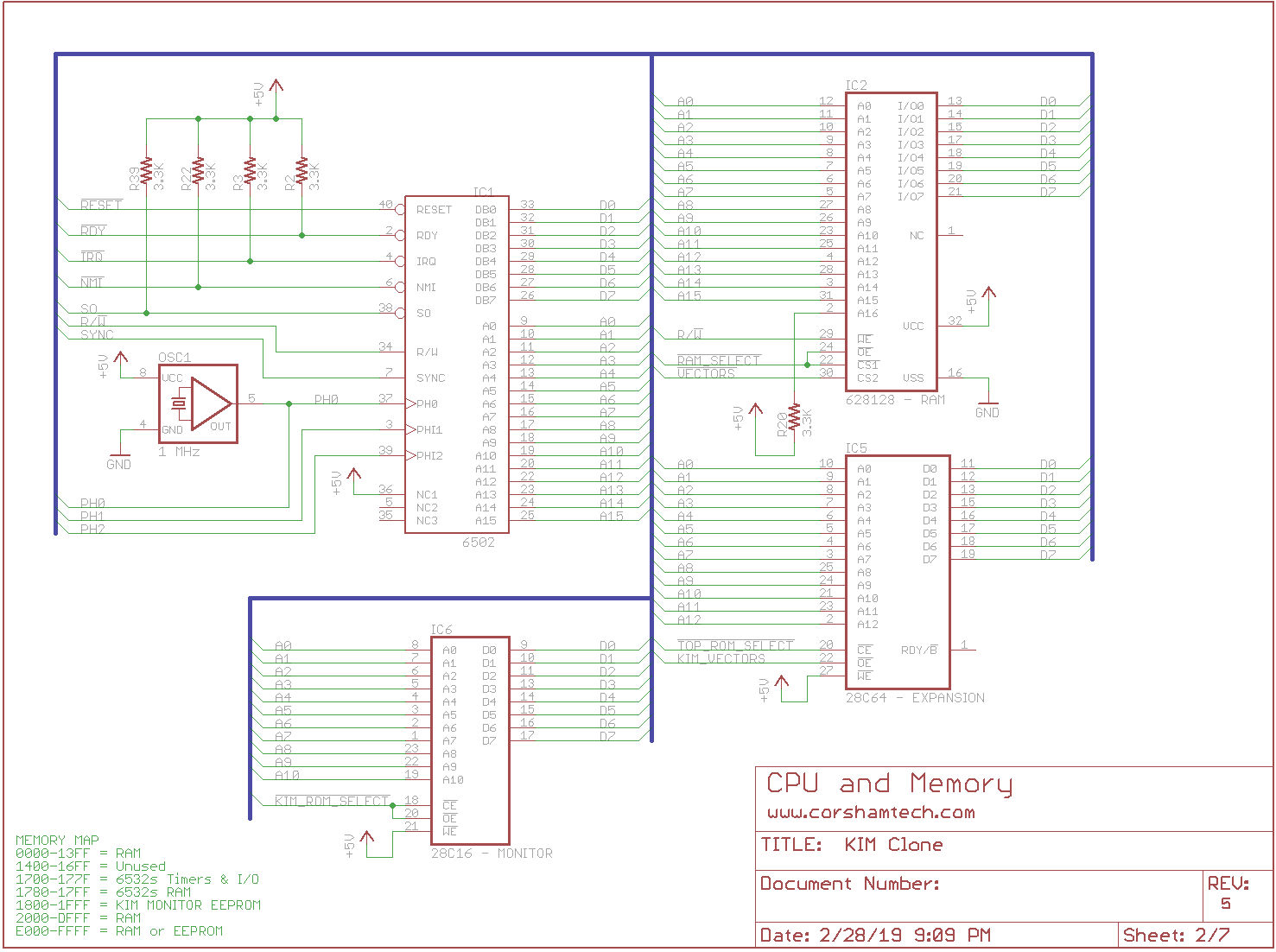
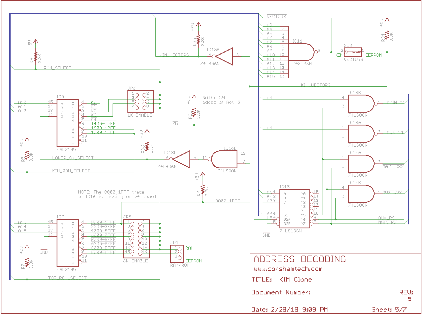
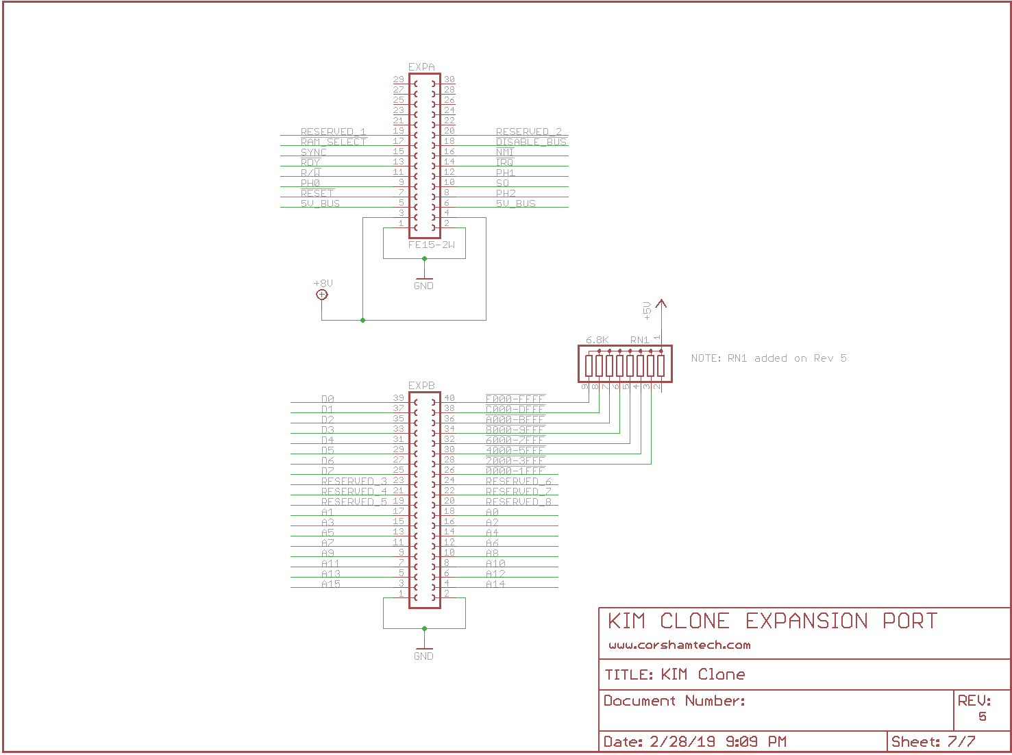
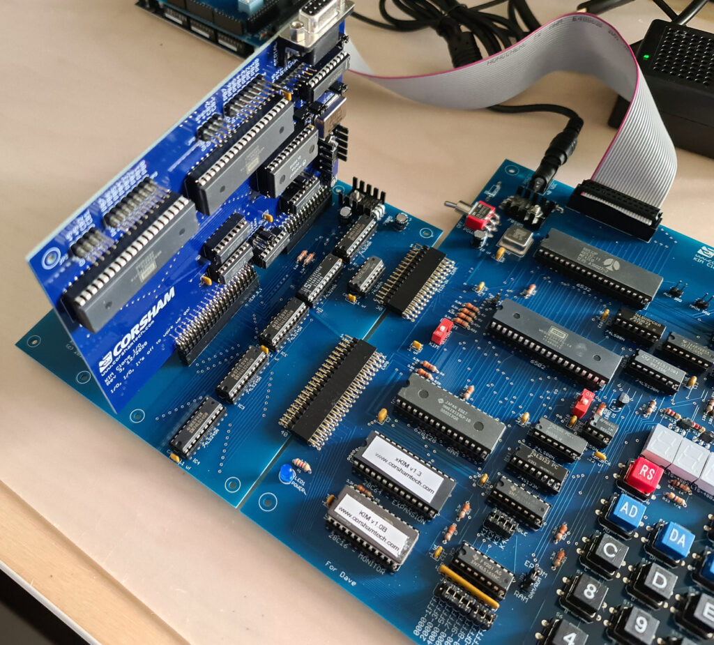
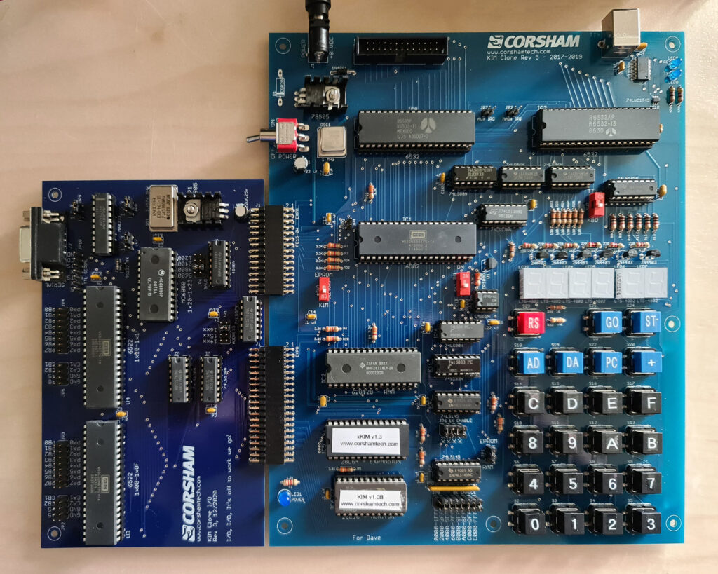
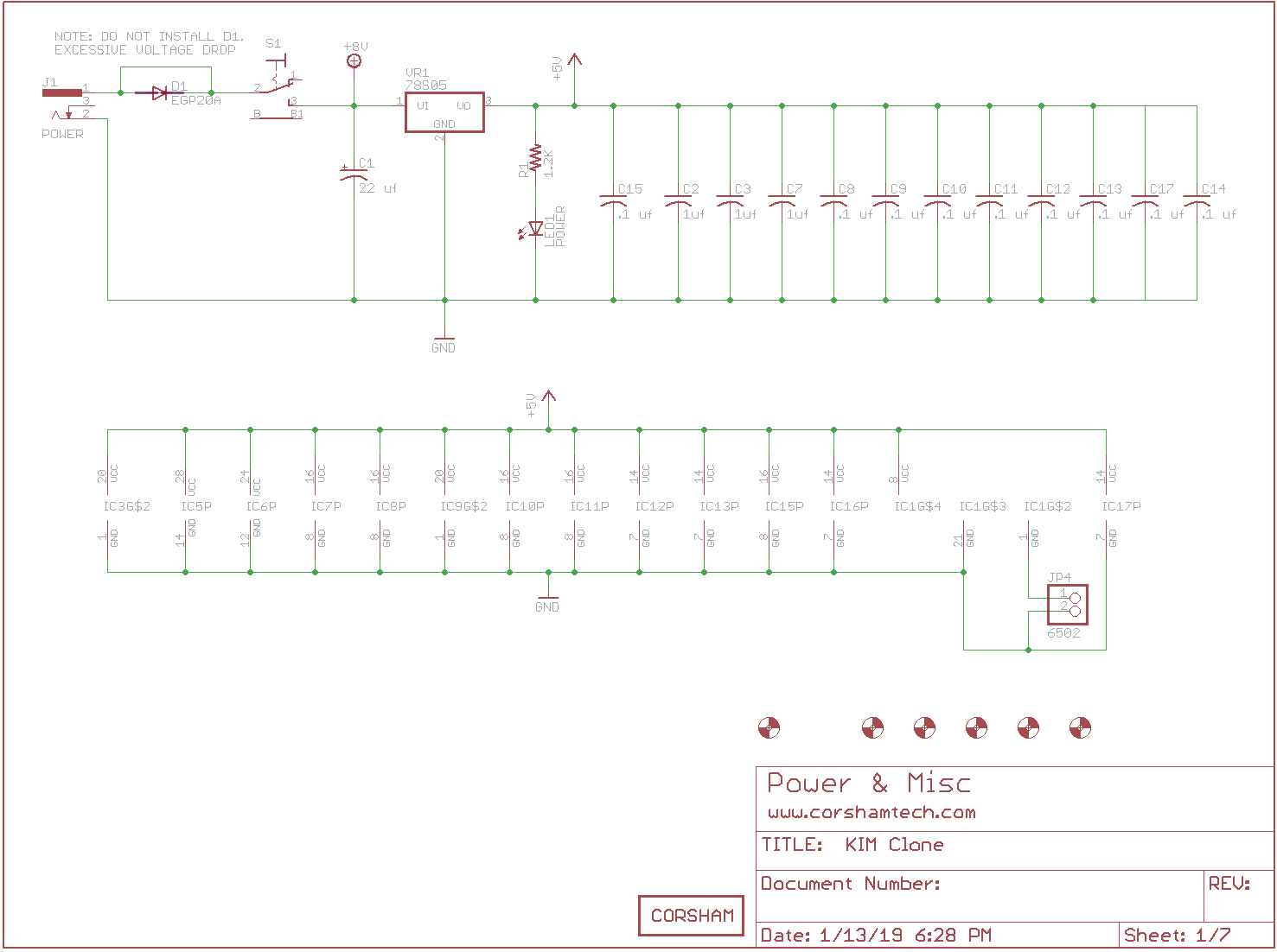
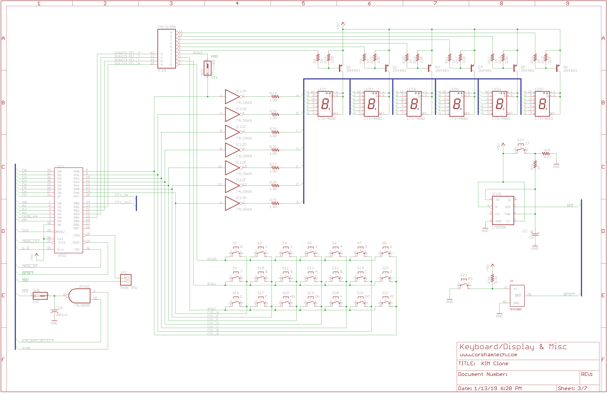
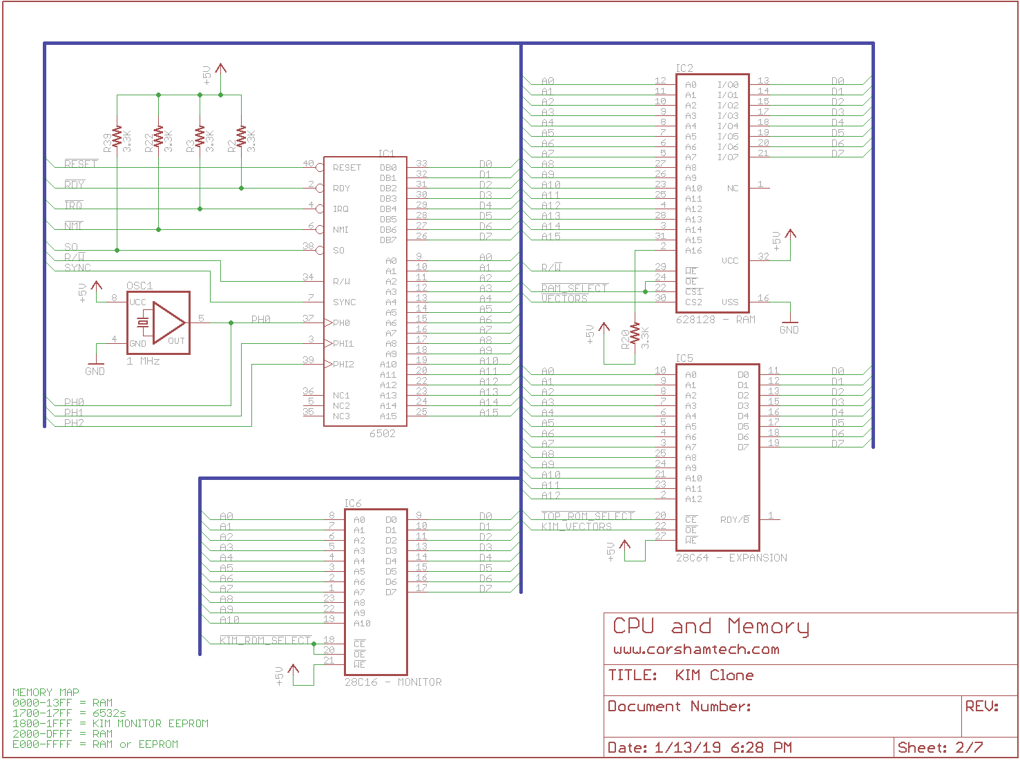
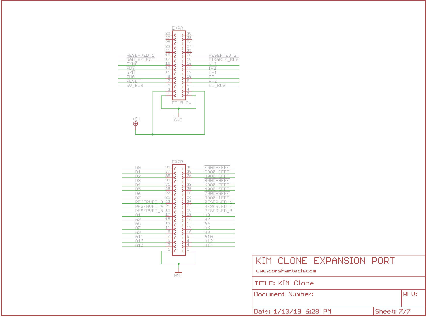
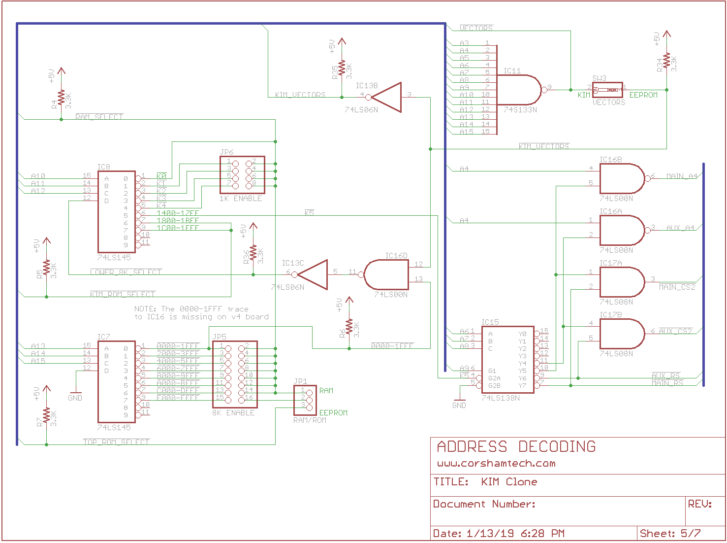
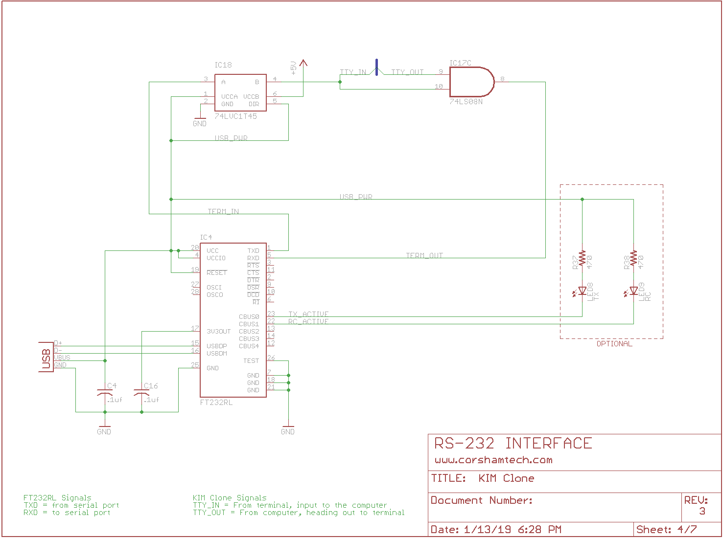
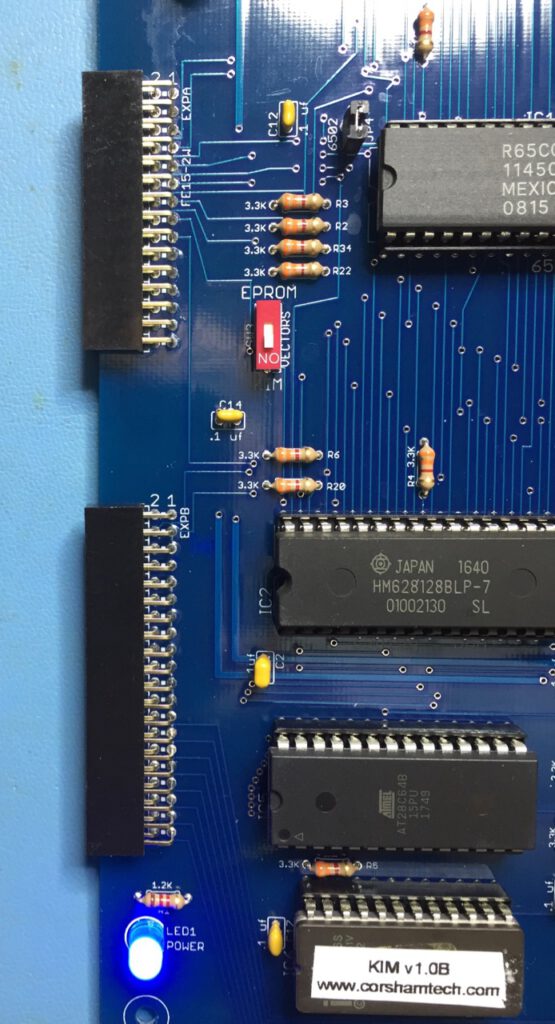
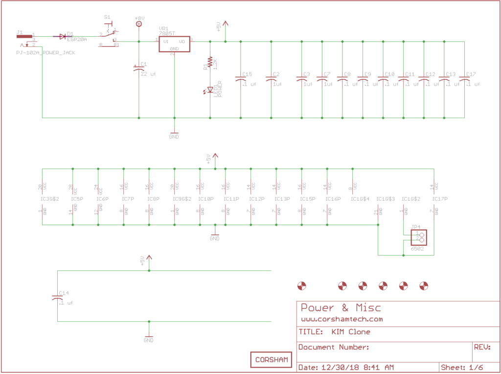
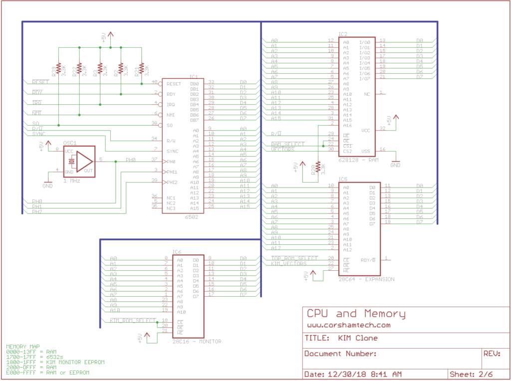
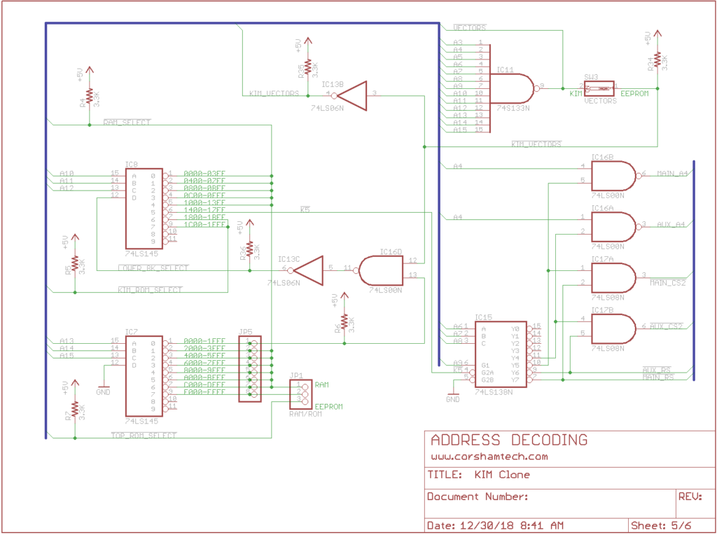
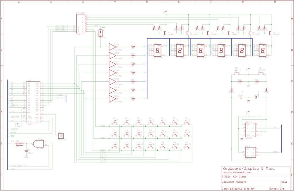
KIM Monitor
# KIM-Monitor
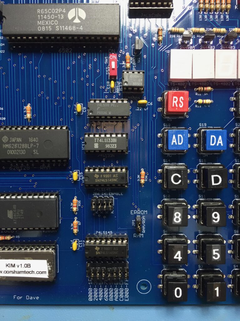
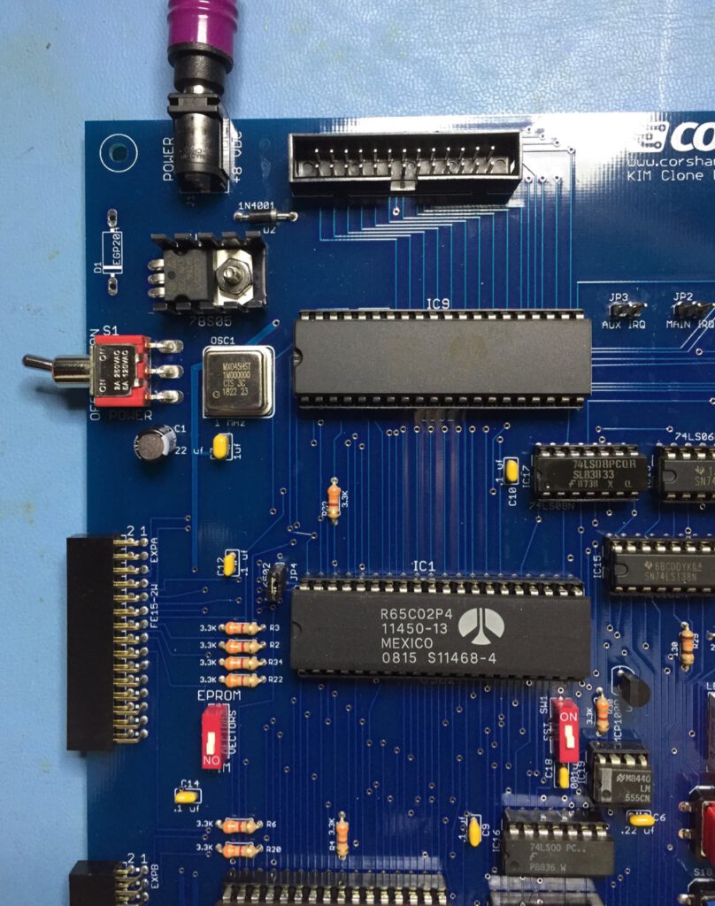
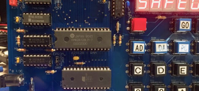
KIM monitor as modified for the Corsham Tech KIM Clone board.
Music Board master
# SS-30 Music Board
This is a rough recreation of the Newtech Computer Systems model 68 music board. No atttempt
was made to make it look exactly like the original, but it is 100% compatible and uses the
same components as the original.
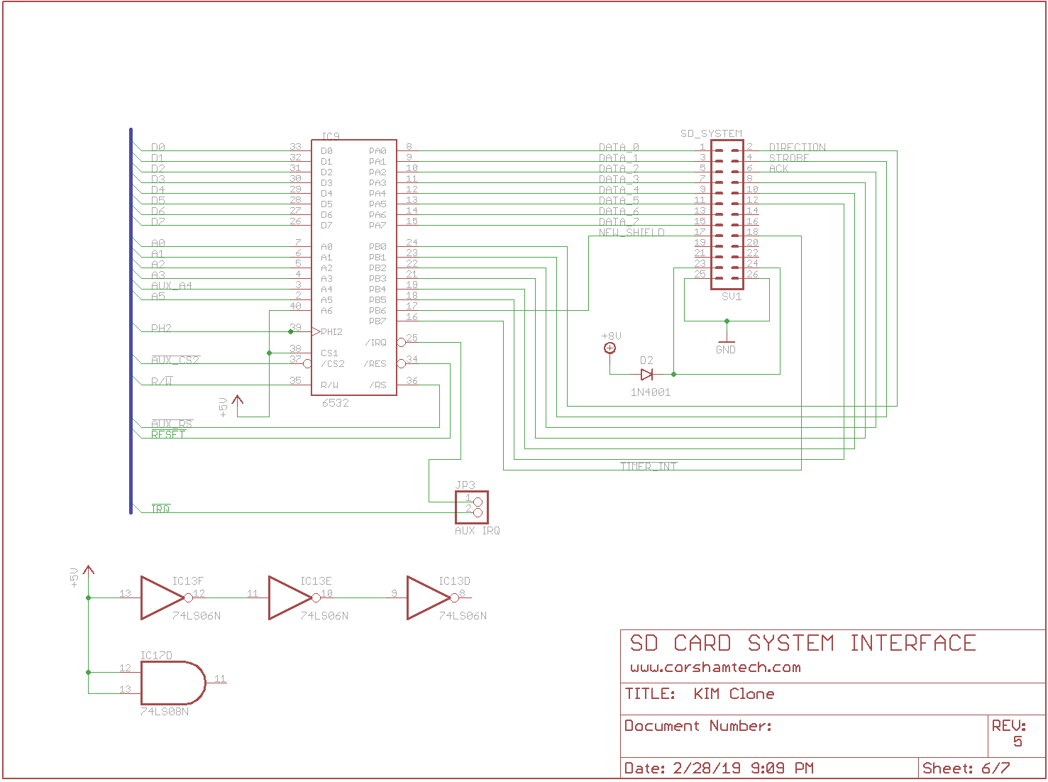
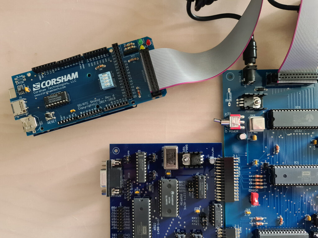
SD Drive
SD Drive Arduino firmware
SD Shield Tester
The SD Shield Tester is a program to test the Corsham Technologies SD Card System shield. This is primarily a manufacturing tool but can be used for general testing. It’s not very useful, but if you suspect an SD Card shield is malfunctioning, this is a way to test it.
xDbg
# xDbg
xDbg is a 65C02 debugger meant to compliment the Corsham Technologies xKIM monitor
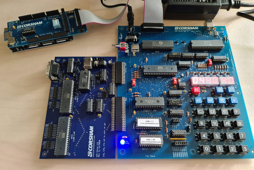
xKiM
# xKIM
xKIM is an extended monitor for KIM computer systems. Commonly used in Corsham Technologies KIM-1 add-on boards.
It is a 6502 based monitor which has basic tools as well as some additional commands for working
with the Corsham Tech SD Card system.
xSBUG
xSBUG
This is the Corsham Technologies version of the SWTBUG SBUG monitor for the 6809. It is close to the original but has support for the Corsham Tech SD Card System (emulates disk drives).
xSWTBUG
xSWTBUG
This is a modified version of the SWTPC monitor SWTBUG for use on their 6800 based SS-50 systems. It has additions for the Corsham Tech SD card subsystem and other minor improvements.