I know of seven KIM-1 revisions, labeled Rev A-G and the first one unlabeled. Rev C is unknown!
What changed between these revisions?
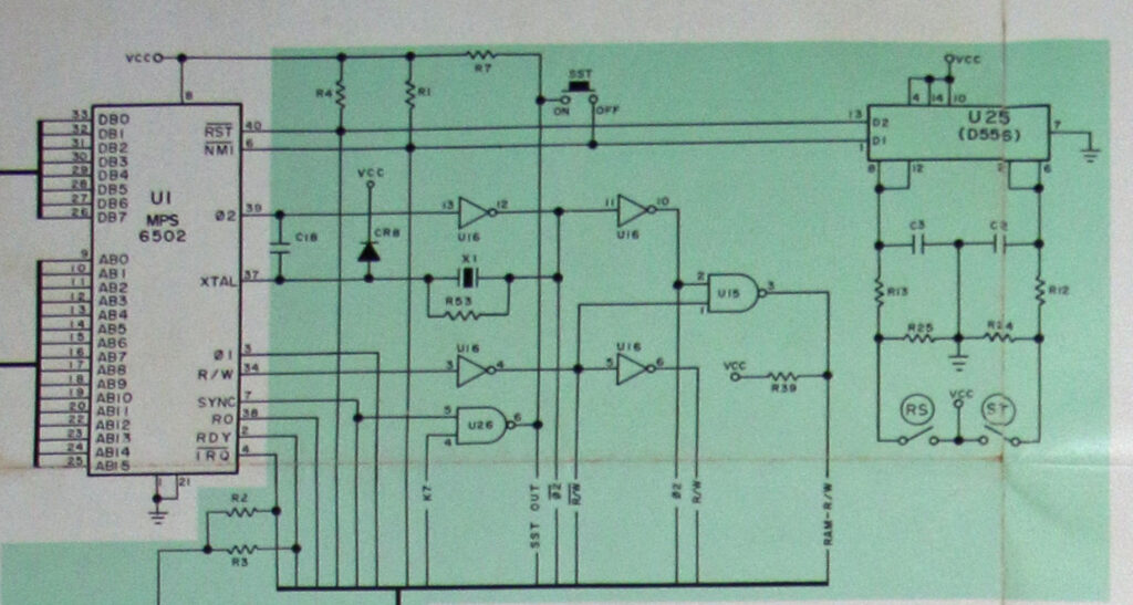
Not much. The PCB underwent several changes around the logo area, from KIM-1 MOS to Commodore C-MOS. That happened from Rev A to Rev D, indicating the takeover by Commodore of MOS Technology. And some small numbers/artefacts etched in various Revs. The big change was in the clock circuit between the first edition and Rev A.
Some have serial numbers, the first ones on the back on the right, later had stamped/written numbers like PAxxx (Palo Alto) and SCxxx (Santa Clara) of Commodore production facilities
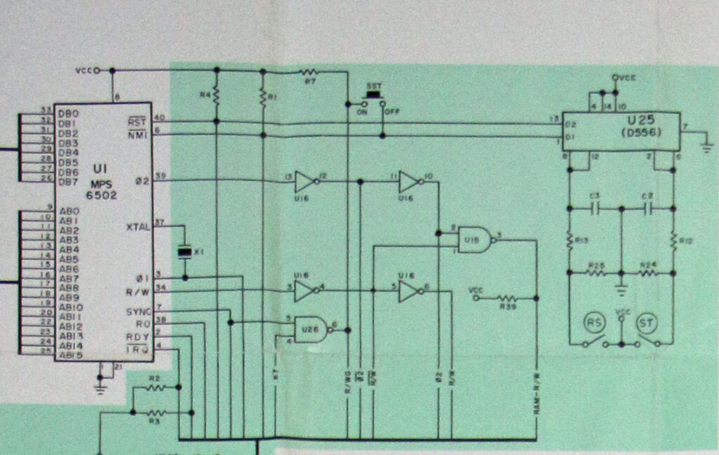
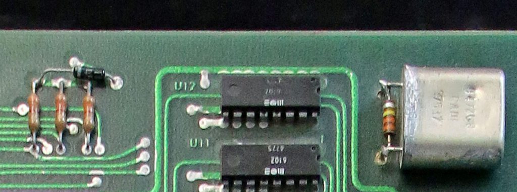
Clock circuit change
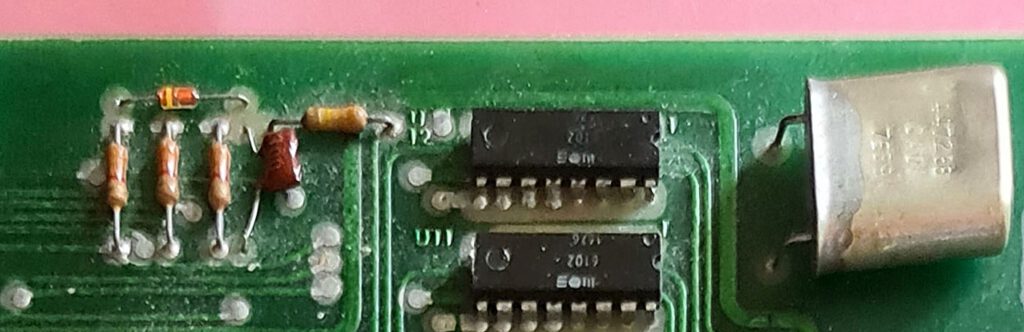
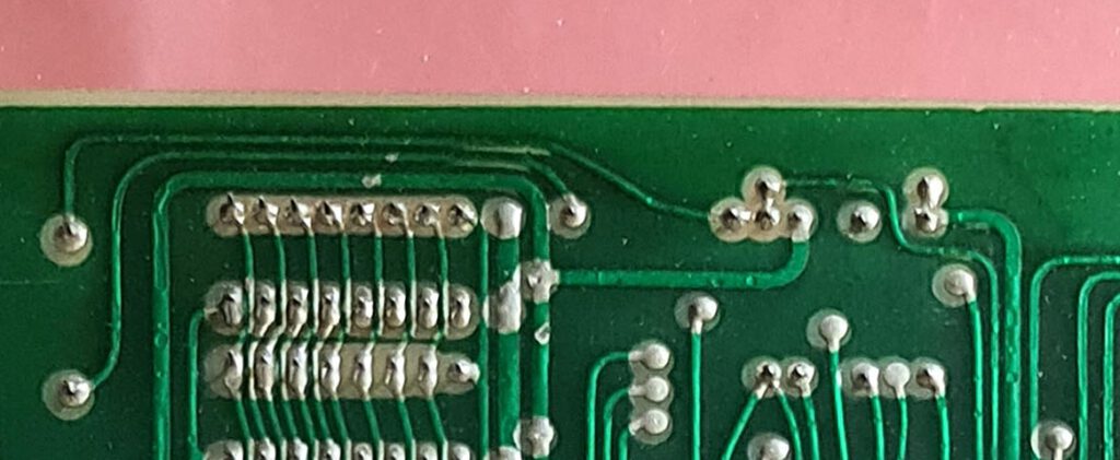
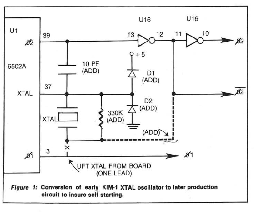
The first batch of KIM-1 suffered from the issue that the clock would not start. It was fixed in Rev A, with more components and a change in PCB layout.The change was also made in the circuit diagram as you can see in the images below.
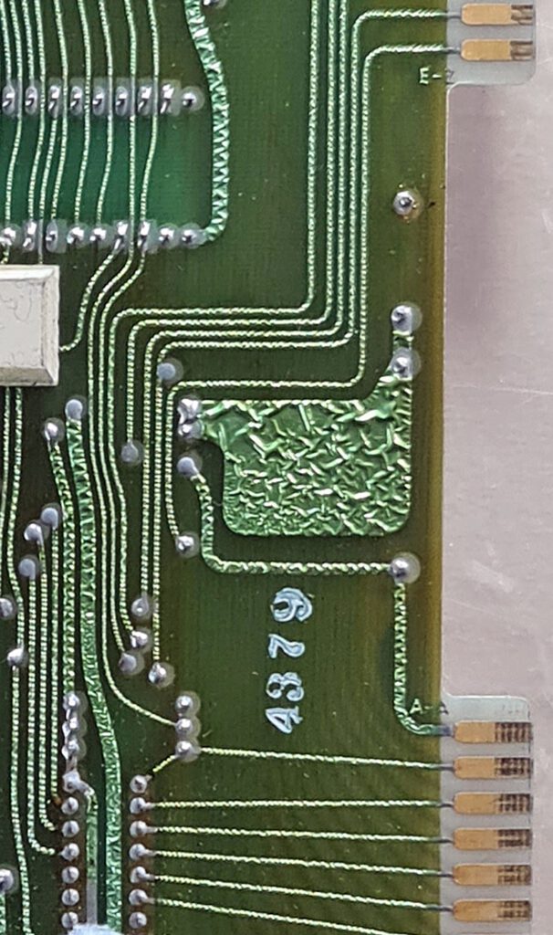
First KIM-1 (I call it first edition)
Here the crystal is connected between pin 3 and pin 37 without any other components.
On my first edition the change was already ‘patched’ on to the KIM-1.
Rev A
More components were added, like resistors, diode and capacitor and pin 3 was left alone in the oscillator circuit.
MICRO JOURNAL letter sent to the editor July/September Issue 38 and 40 1981
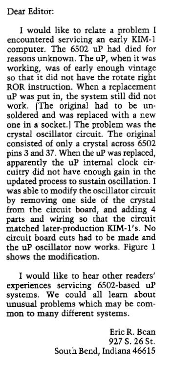
There was a change in the PCB from Rev A to B.
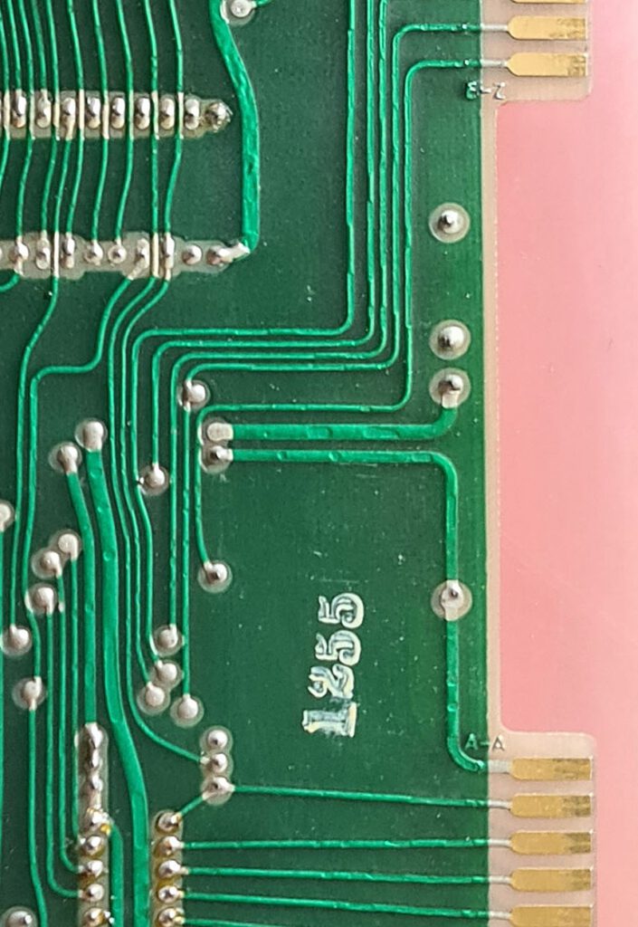
Rev A
Rev B
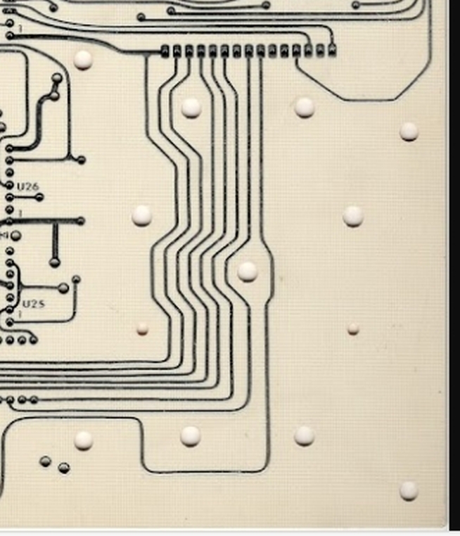
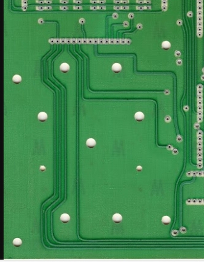
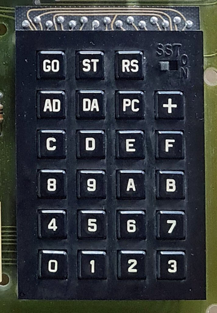
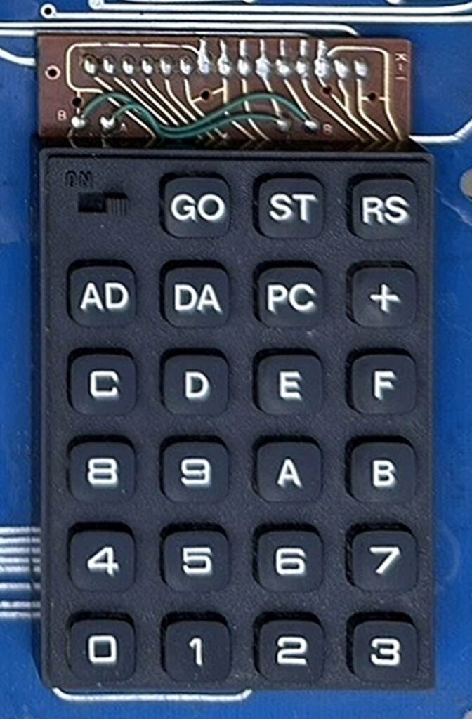
Another change appeared going from Rev B to Rev D. The keyboard changed, the SST switch moved to the other side. And there were some extra holes required for the new keybaord, some traces needed to move also.
Rev A front keyboard

Rev A back keyboard
Rev D front keyboard
Rev A back keyboard
The User Manual went from version 15 (January 1976) to 15A (March 1976) to 15B (August 1976) without significant changes, mostly typing errors and the change of keyboard from Rev B to Rev D.
The keyboard changed from rev B to Rev D. The SST switch moved to the other side, the first Rev keyboards were not very reliable.
Rev B
Rev D
What did not change?
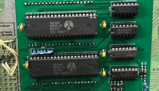
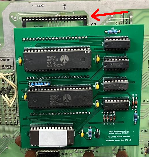
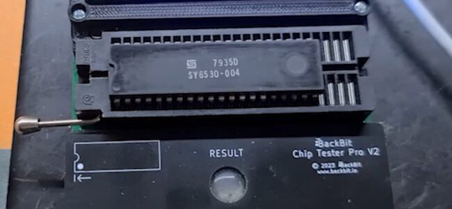
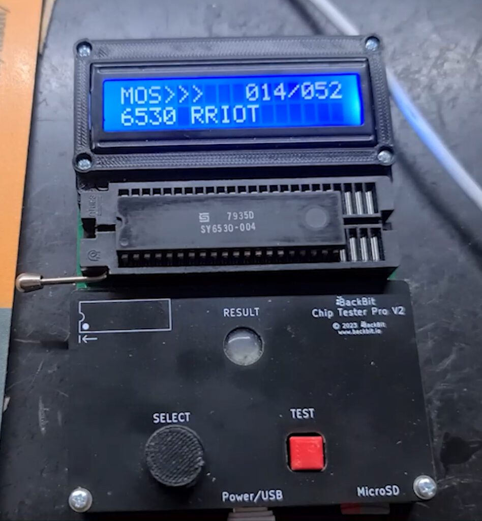
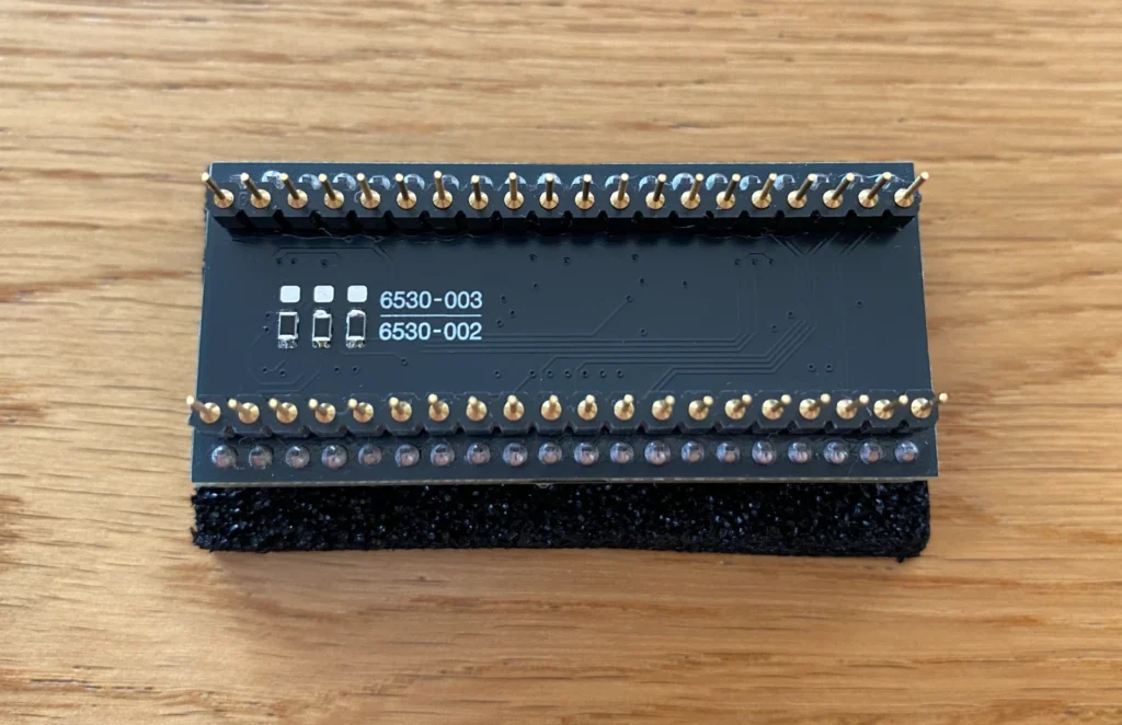
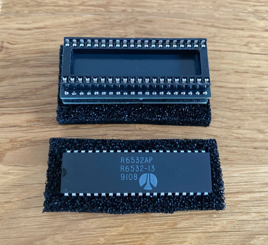
The 6530 – 002 and -003 were from many different dates between 1976 and 1980. The functionality stayed the same, no software changes are known. It seems the same mask was used to produce another batch due to the demand for KIM-1s. On Rev F and G I have seen older 6530s (ceramic ones) from much earlies dates, old stock being used?
The large Circuit Diagram poster stayed the same for all revisions as far as the circuit itself. Colors changed to only blue background in the last revisions.
Parts used
The parts used in all these revisions changed from as much as possible made by MOS Technology (6102) to industry standard compatible types (2102). E.g the RAM ICs were all third party in later revisions.
The capacitors, mostly yellow tube types, also came in various colors and sources between revisions.
Except for Rev G no IC sockets were used.