Jim Butterfield
Aug 19, 1999, 9:00:00 AM
to
Joe Forster/STA wrote:
>
> Can you, please, explain me in short what this KIM-1 machine
> is: CPU, RAM, video, sound, periphery, lookout, startup
> screen, programming? A URL would also be fine, I guess…
> I haven’t seen a KIM-1 before… Thanks in advance!
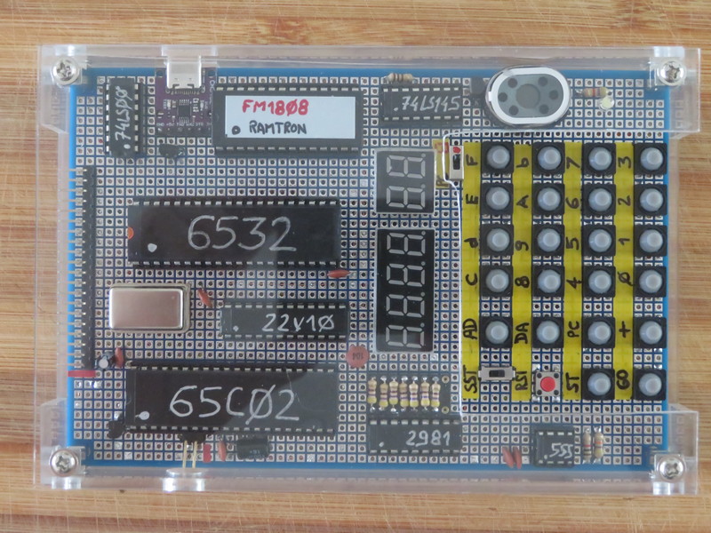
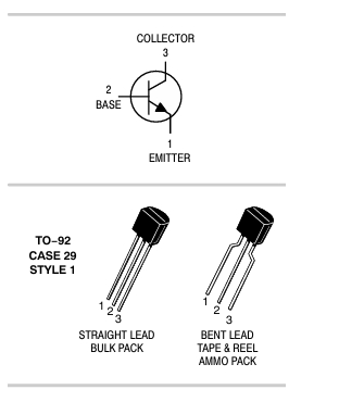
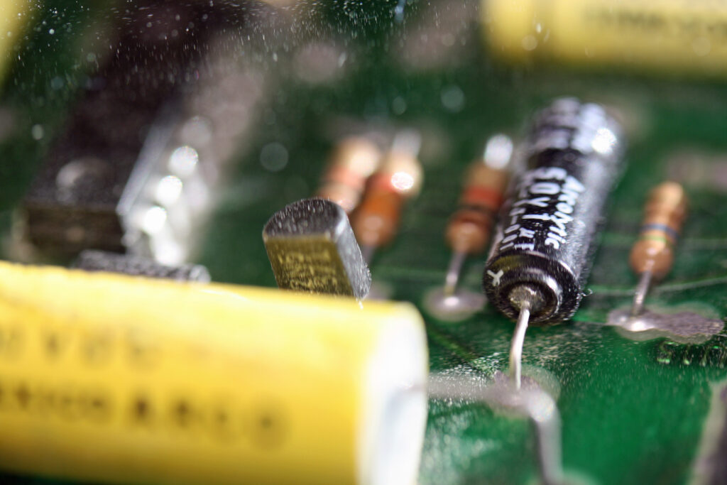
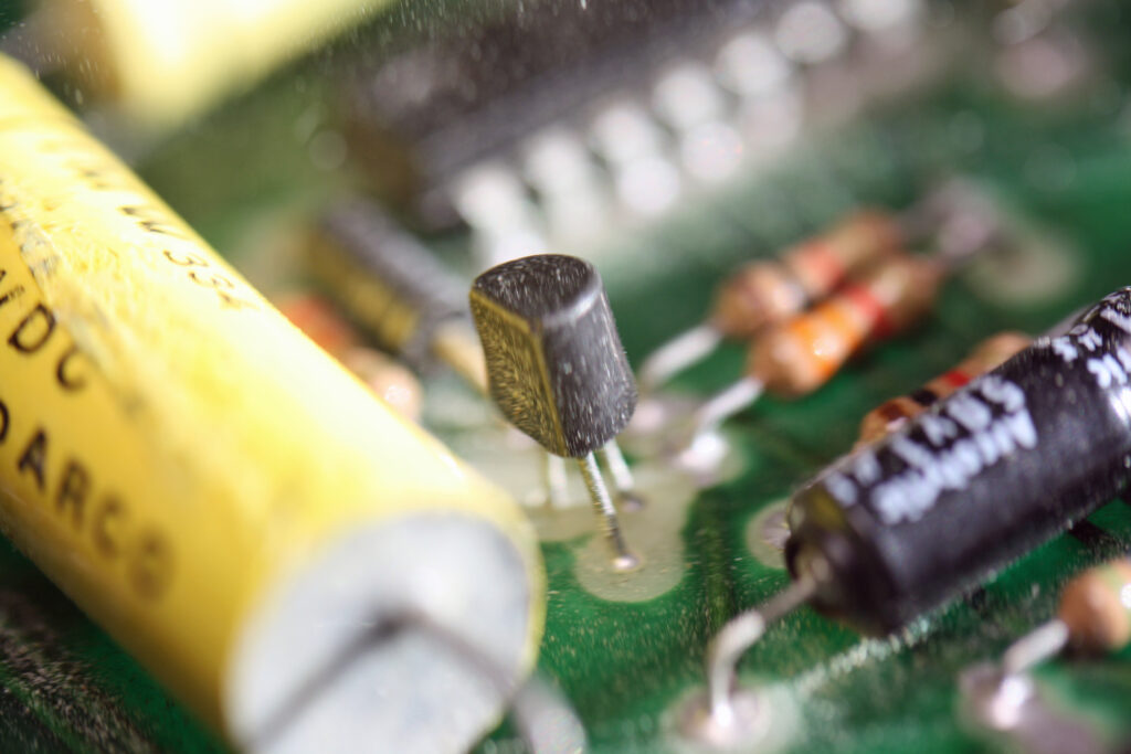
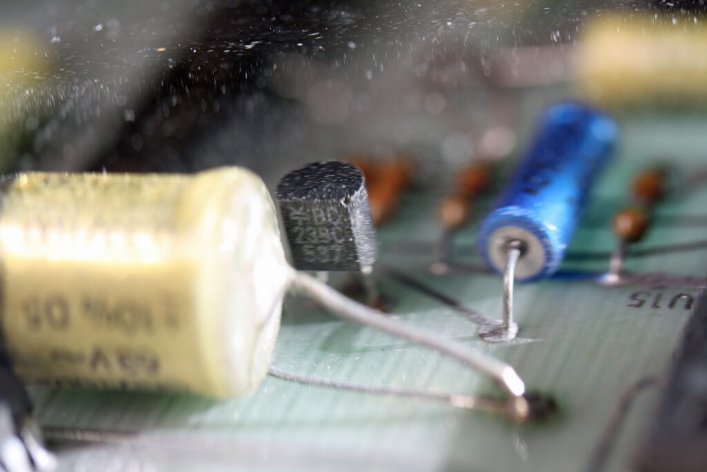
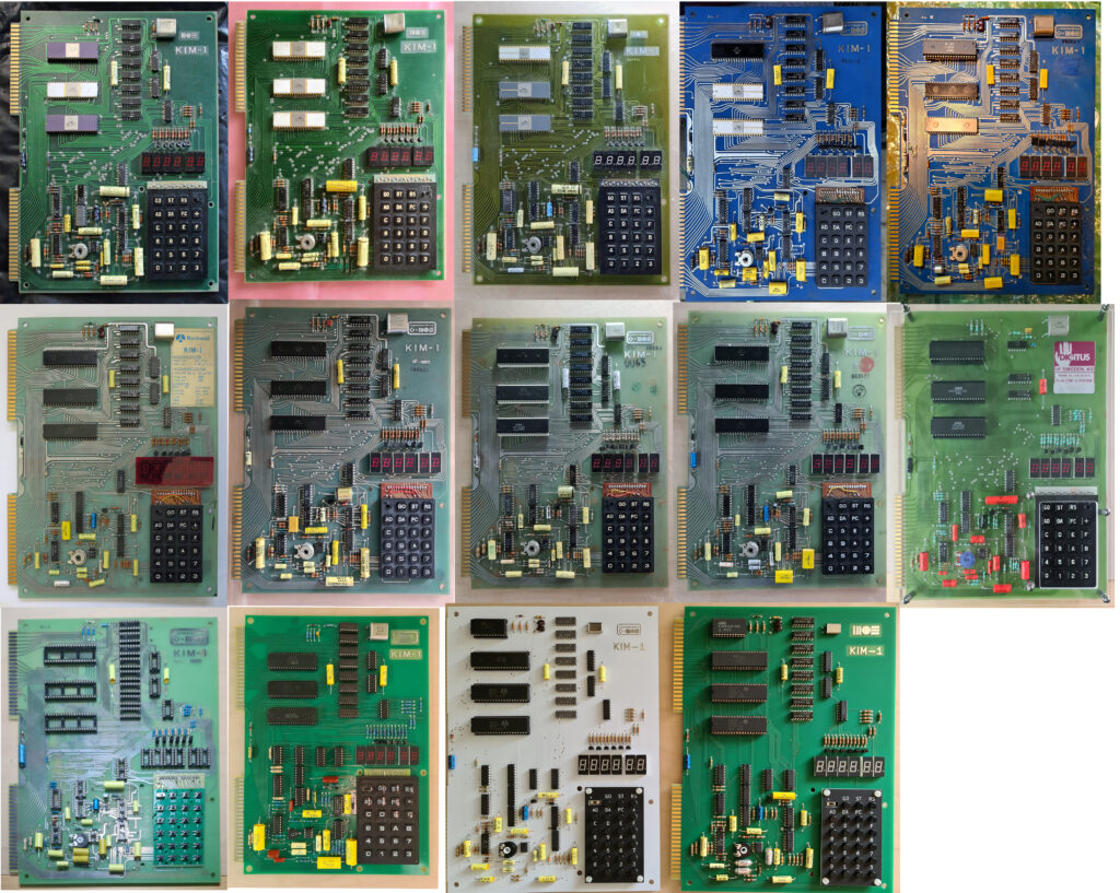
Shortly after MOS Technology, Inc. developed the 6502 processor chip,
they designed a single-board computer called the KIM-1 to show off the
capabilities of the chip family, and to allow engineering prototyping.
Apart from the obvious things that a computer must have (CPU, RAM, I/O
chips), they threw on the board just about anything that they thought
someone might like to have as an interface. For example: the basic
monitor program allowed a hex keypad input (hey, KIM stands for Keyboard
Input Monitor) and 6-digit LED display; it had a bit-banger audio output
which could be used to store programs on a cassette tape unit; it had a
corresponding PLL audio input line that would read back from such a
cassette tape; and it had teletype input/output facilities (again,
bit-banger). Its basic RAM was 1K, supplemented by a little extra RAM in
the 6530 I/O chips.
A feature of the board that many users never realized, perhaps, is that
all on-board devices were selectable via external connections. What that
means is that you could plug the KIM-1 board into a mother housing, which
could, as desired, disconnect any or all of the peripheral circuits, I/O
chips, RAM, or the ROMs containing the monitor.
It’s likely that MOS Technology designed the board as a tool for
engineers, with the message “Hey, design your own system and copy the
things you like from this board”. I suspect they were quite amazed when
sales started to approach the 100,000 mark!
Here’s my take on what happened: computer hobbyists discovered that, for
the first time, there was a standard preassembled board that would be the
same for all users. Back in those days, most computers came as a printed
circuit board and a bag of parts which you had to assemble yourself.
More, everybody made a slightly different system: some had a CRT
display, some had LEDs, some had teletype; varying amounts of memory were
fitted, mapped to a variety of addresses; and operating systems were
whatever you could scare up.
But suddenly there was the KIM-1. It was fully assembled (although you
had to add a power supply). Everybody’s KIM-1 was essentially the same
(although the CPU added an extra instruction during the KIM-1’s
production life).
And this created something that was never before part of the home
computer phenomenon: users could quite happily exchange programs with
each other; magazines could publish such programs; and people could talk
about a known system.
We knew the 6502 chip was great, but it took quite a while to convince
the majority of computer hobbyists. MOS Technology offered this CPU at a
price that was a fraction of what the other available chips cost. We
faced the attitude that “it must be no good because it’s too cheap,” even
though the 6502, with its pipelined architecture, outperformed the 8080
and the 6800.
The arrival of the KIM-1 and its user group was, I think, a landmark in
early personal computer history.
–Jim
Post from here