
By Bob Applegate
KIM Clone I/O Not Receiving Serial Data
While testing the KIM Clone I/O Board I was using a real ASCII terminal and everything was working exactly as it should. After the board was in product a dedicated tool was written to run complete tests of the board and the serial port was no longer receiving data.
As it turns out, it is possible to set the various jumpers on the board so that the DCD line on the 6850 is floating, and it tends to float to a state where it ignores incoming data. My test jig simply loops back pins 2 and 3, leaving DCD unconnected.
The easiest solution is to pull the jumper off JP8, then place it between pins 6 and 7 on JP10. This forces the DCD to ground, which allows the receiver to work as expected.
Depending on your application, whatever is connected to the DB-9 might pull DCD to the active state which also allows the receiver to work properly.
Future revisions of the board will have a pull-down resistor on both DCD and CTS so unconnected inputs will default to the proper levels for normal operation of the ACIA.
Using I/O lines
Like the original KIM-1, there are 16 I/O lines on the KIM Clone that can be used for your own projects. They are brought to the connector labeled “SD SYSTEM” along the top edge of the board and were meant to plug into one of our SD Card Systems for program storage. However, they are general purpose I/O lines which can be freely used for other things if the SD system is not used.
This is a portion of the schematic showing which pins on the 6532 are connected to which pins on the connector:
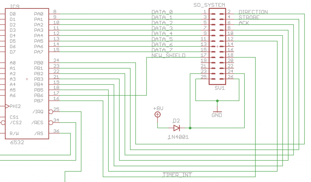
Don’t worry about the signal names associated with the various lines, they are the names of those signals when an SD Card System is attached.
As you can see, there are 16 IO lines, 2 ground lines, and 2 lines with +7.5… if you want to draw power from this connector for TTL/CMOS circuits then you need to add your own +5 volt regulator! D2 prevents back-feeding power from the connector back into the KIM Clone.
On the circuit board, pins 1 and 2 are labeled but are covered by the connector, so here is a reference:
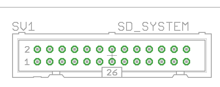
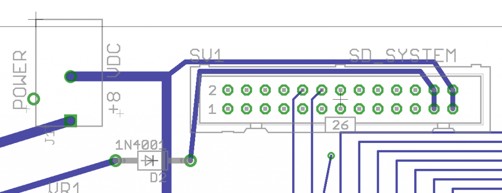
All of the odd numbered pins are on the “bottom” row while even numbered pins are on the top. Ie, the top row has pins 2, 4, 6, etc, while the bottom row has 1, 3, 5, etc. Displaying the circuit board traces on the bottom layer of the board you can clearly see the ground and power lines connected to the pins on the far right:
The datasheet for the 6532 RIOT chip is readily available here.
To program the chip you basically need to set the direction of each pin of the I/O port of interest (Port A or Port B), then set the data or read the data. The base address of the chip is 1700 (hex). There are four registers:
| Address | Use |
| 1700 | Data register A |
| 1701 | Data direction register A. Setting a bit to 1 makes it an output bit, 0 makes it an input. |
| 1702 | Data register B |
| 1703 | Data direction register B. Setting a bit to 1 makes it an output bit, 0 makes it an input. |
An Example
I needed to test experimental address decoder logic and found it was easier to just plug it into the I/O ports and write some code on the KIM Clone to simulate the addresses and display what the decoder logic did:
Port A simulates address lines A11-A16 and port B has the three decoder outputs (/RAM, /IO, /EEPROM). A small program simulates all possible values of the five address bits, displays the address, reads the decoder inputs and then displays which are active. In about an hour I was able to fix one minor bug in the decoder design and perform a full unit test on how it works. Certainly not a fancy example of using I/O ports, but sometimes it far faster to build a small circuit and use software to test it rather than building a lot of hardware and manually debugging it all.