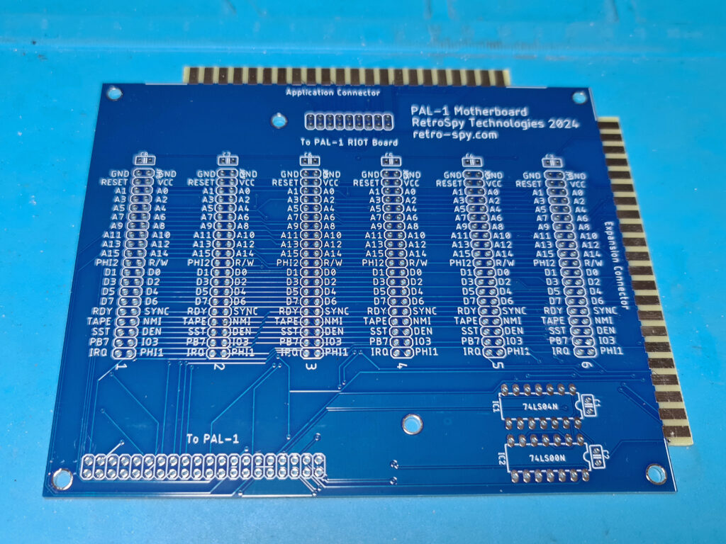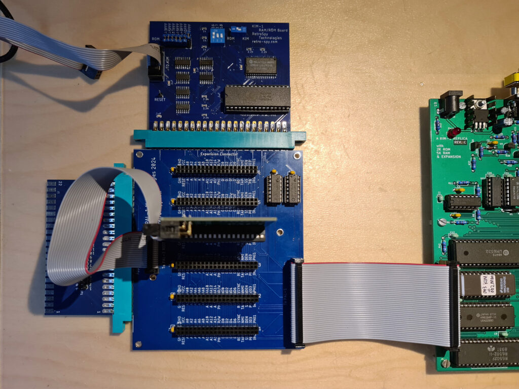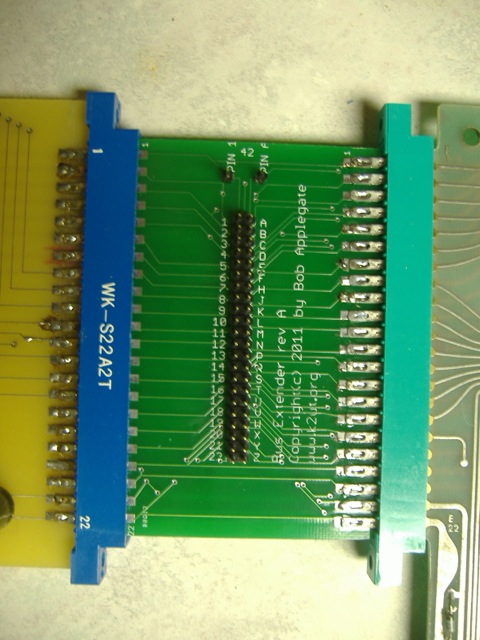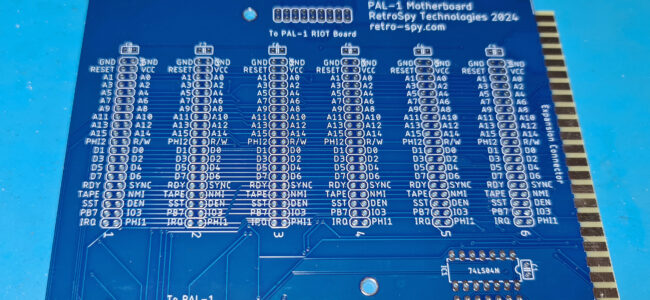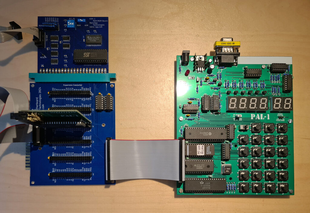
The PAL-1 connected to the PAL-1 Motherboard Expansion kit
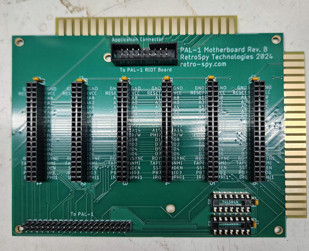
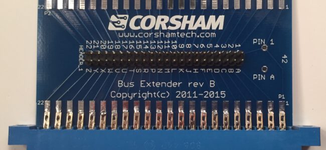
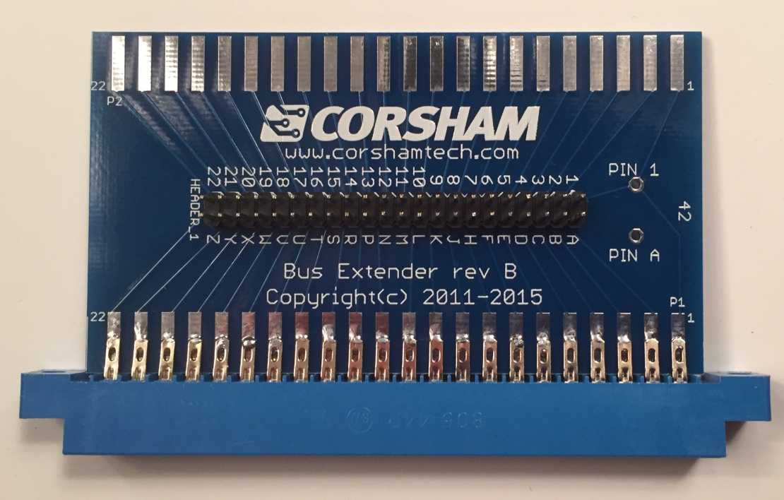
Revison B with larger edge fingers
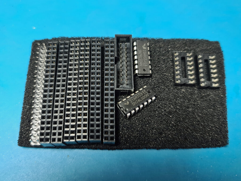
I bought this kit from
Retrospy Technologies and built it to enhance my PAL-1.
Worthwhile to add not only a motherboard but also get KIM-1 Expansion and Application connectors!
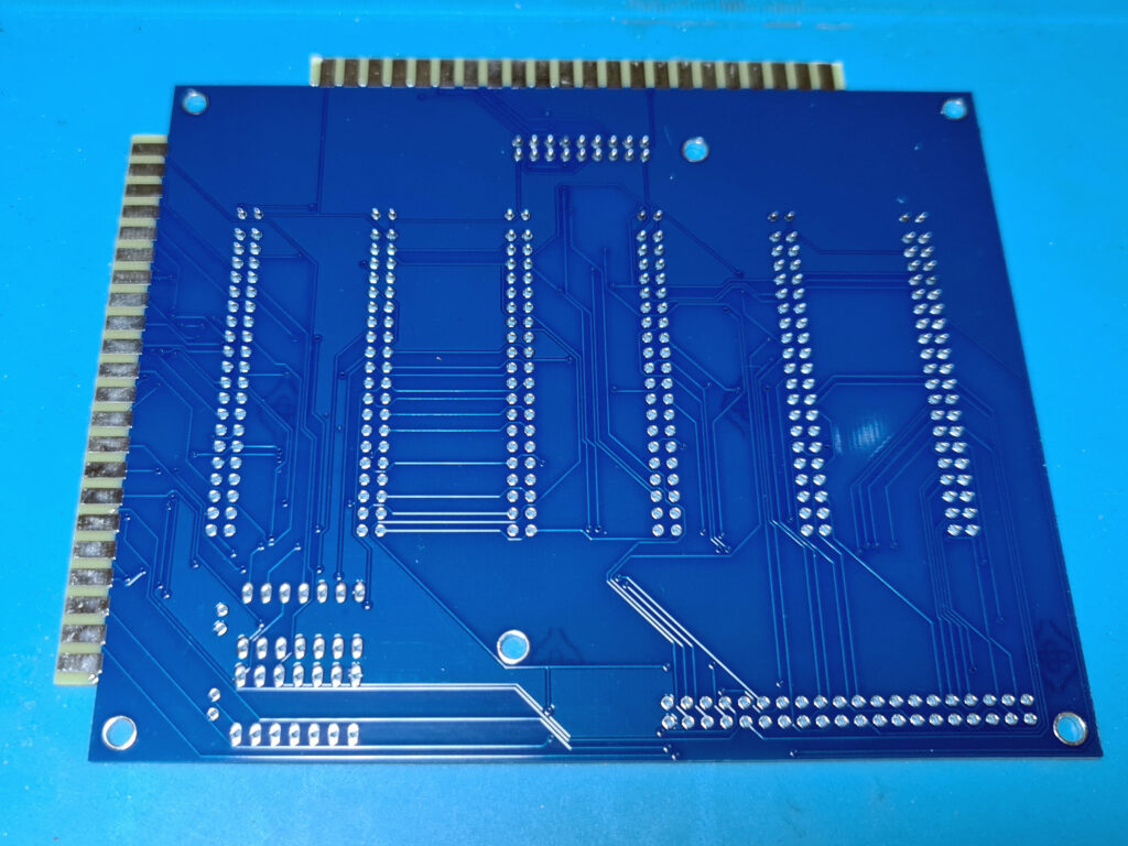
Easy to build, high quality PCB, lots of points to solder with the six PAl-1 Motherboards connectors.
Description from the Retrospy store:
With this motherboard, you can connect up to 6 expansion boards to your PAL-1 at the same time. The motherboard also provides the Application and Expansion connectors found on the original KIM-1, enabling the use of original KIM-1 expansion boards.
NOTE: To do anything worthwhile with the Application connector you will need the PAL-1 2nd RIOT Expansion Kit.
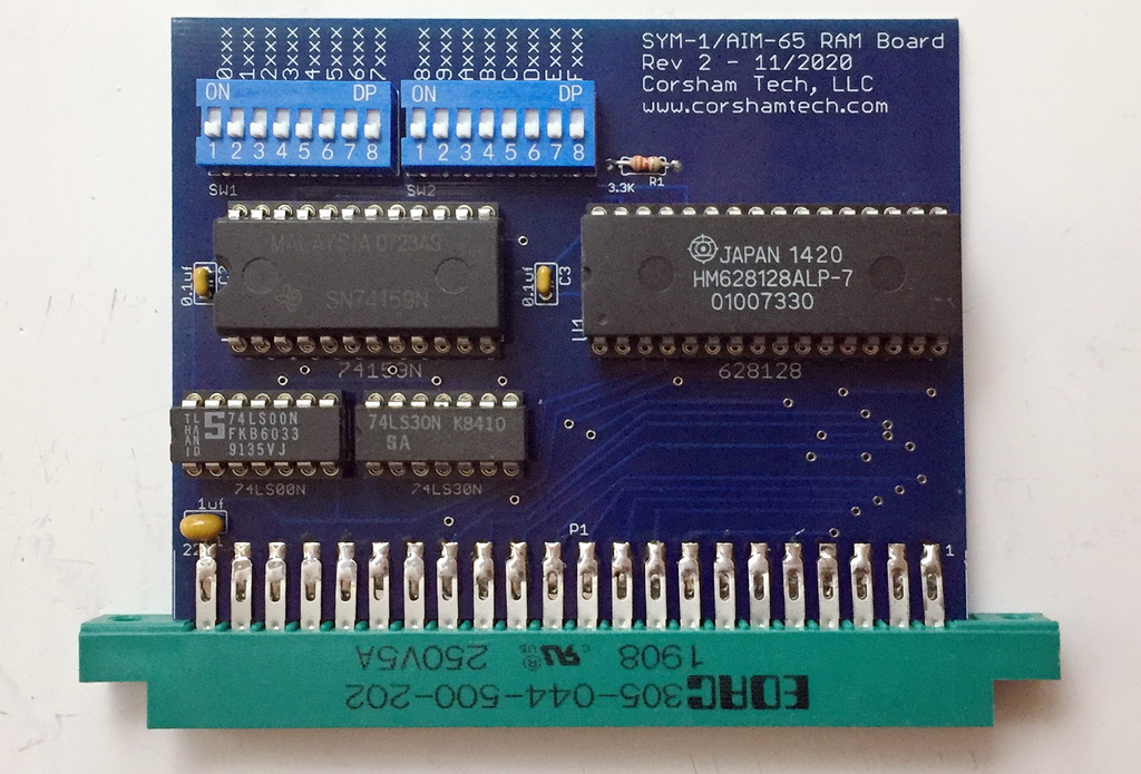
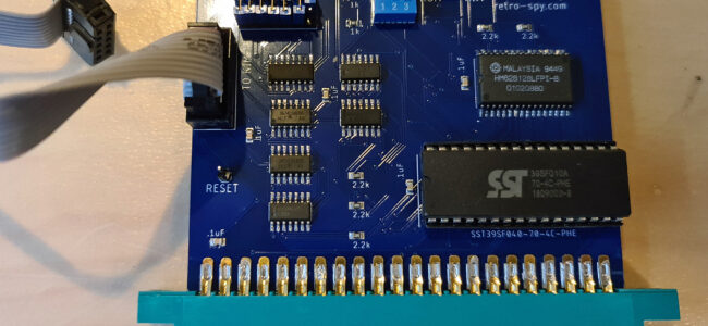
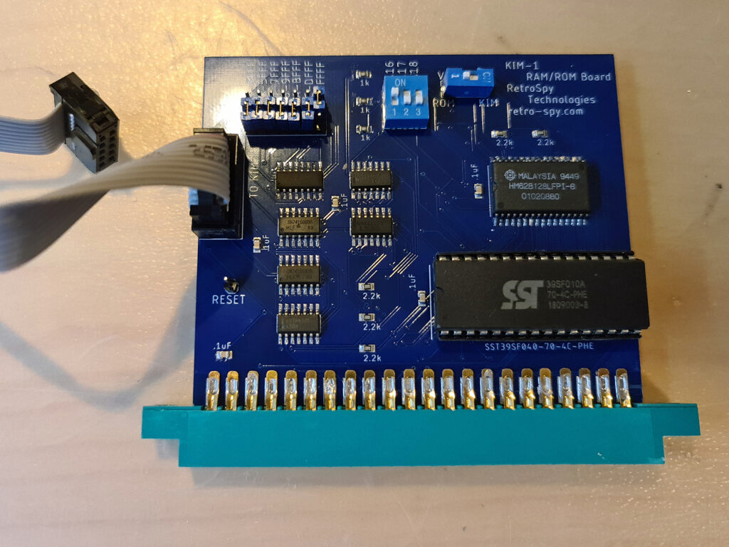
Not all signals are routed to the Application and Expansion connectors because the PAL-1 doesn’t provide them, so there is no guarantee every expansion board will work. However, Corsham Technologies’ and RetroSpy Technologies KIM-1 I/O and KIM-1 RAM/ROM boards have been tested and are compatible.
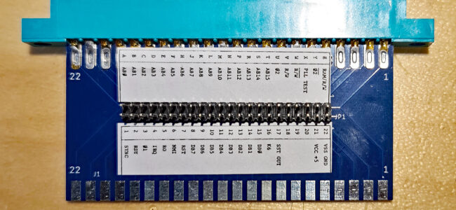
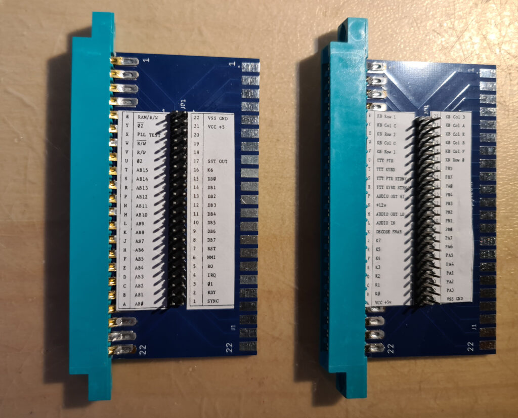
Available signals on the Application connector:
+5V
GND
PA0-7 (with installed PAL-1 2nd RIOT Expansion Kit)
PB0-7 (with installed PAL-1 2nd RIOT Expansion Kit)
DECODE ENAB
Missing are KB Row 0-3, KB Col A-G, TTY KYBD + RTRN, TTY PTR + RTNR, AUDIO Out (lo, hi), AUDIO IN, +12V, K0-K5, K7
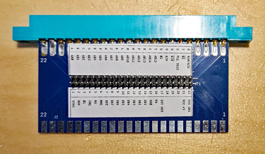
Available signals on the Expansion connector:
+5V
GND
A0-A15
D0-D7
SYNC
RDY
IRQ
NMI
RST
SST OUT
PHI2
R/W
/R/W
/PHI2
RAM/R/W
Missing signals are: K6, SST, RO (pin 38 of the 6502), Phi1 (pin 3 of the 6502), PLL Test. On Reb B Phi1 is also available.
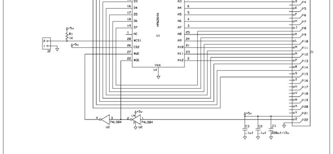
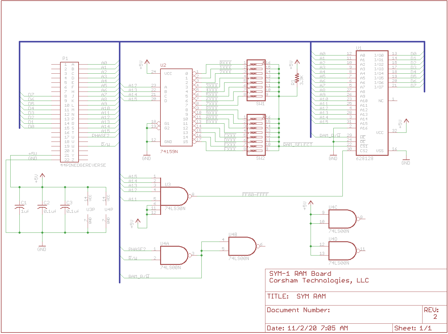
The signals /R/W, /Phi2 and RAM R/W are regenerated with two logic IC’s, the (reverse engineered) circuit is show below. The circuit could be a bit simpler, 3/4 of the 74LS00 would suffice.
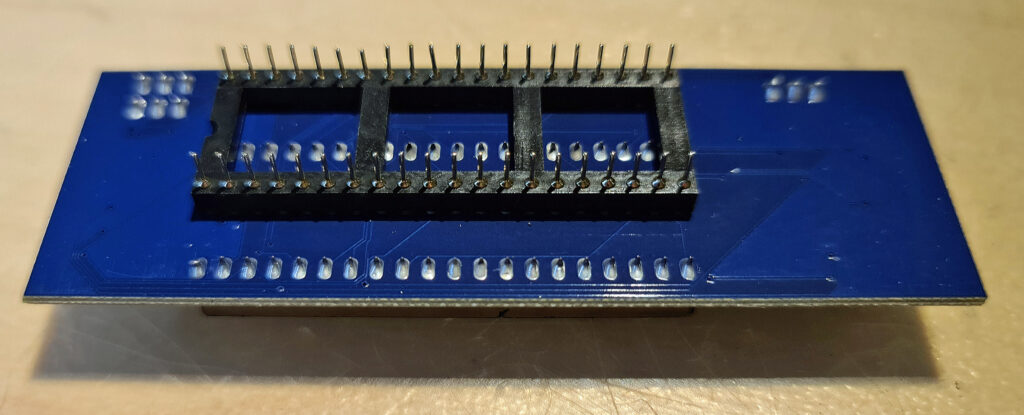
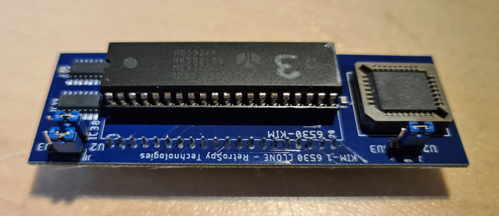
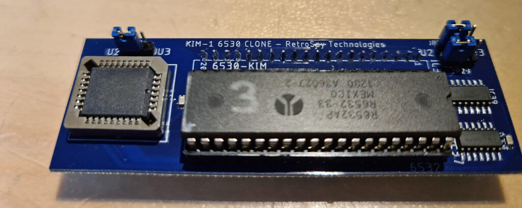
Add KIM-1 RAM/ROM boards
Any KIM-1 RAM/ROM board can be connected to the Expansion connector. The Retrospy KIM-1 RAM/ROM is an excellent one.
For the PAL-1 only the Decode Enable line has to be added. For exammple with one wire Dupont male-female cable, from a motherboard connector. Any RAM in the region 0-1FFF is already available on the PAL-1 itself and should not be enabled on a RAM expansion. And therefore no need for signals K1-K4, the chip select lines for that region.
This version of the expansion kit has some minor points to improve (2.2 will be a next version the designer told me):
– add Phi1, not used often but is available on the PAL-1 connector
– enlarge the PCB edge pads with some mm’s, KIM-1 boards detach now to easy
– the two logic IC’s can easily be replaced with one 74LS00, only one NAND port and two inverters are required
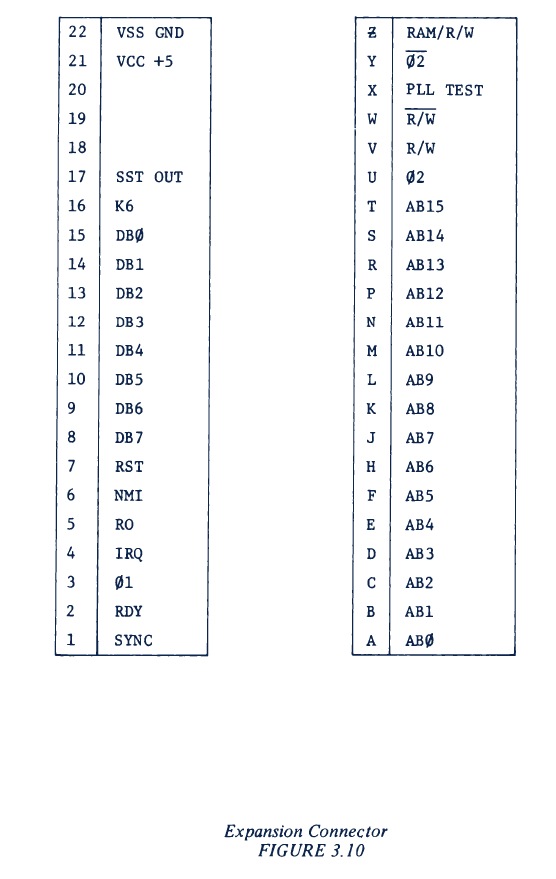
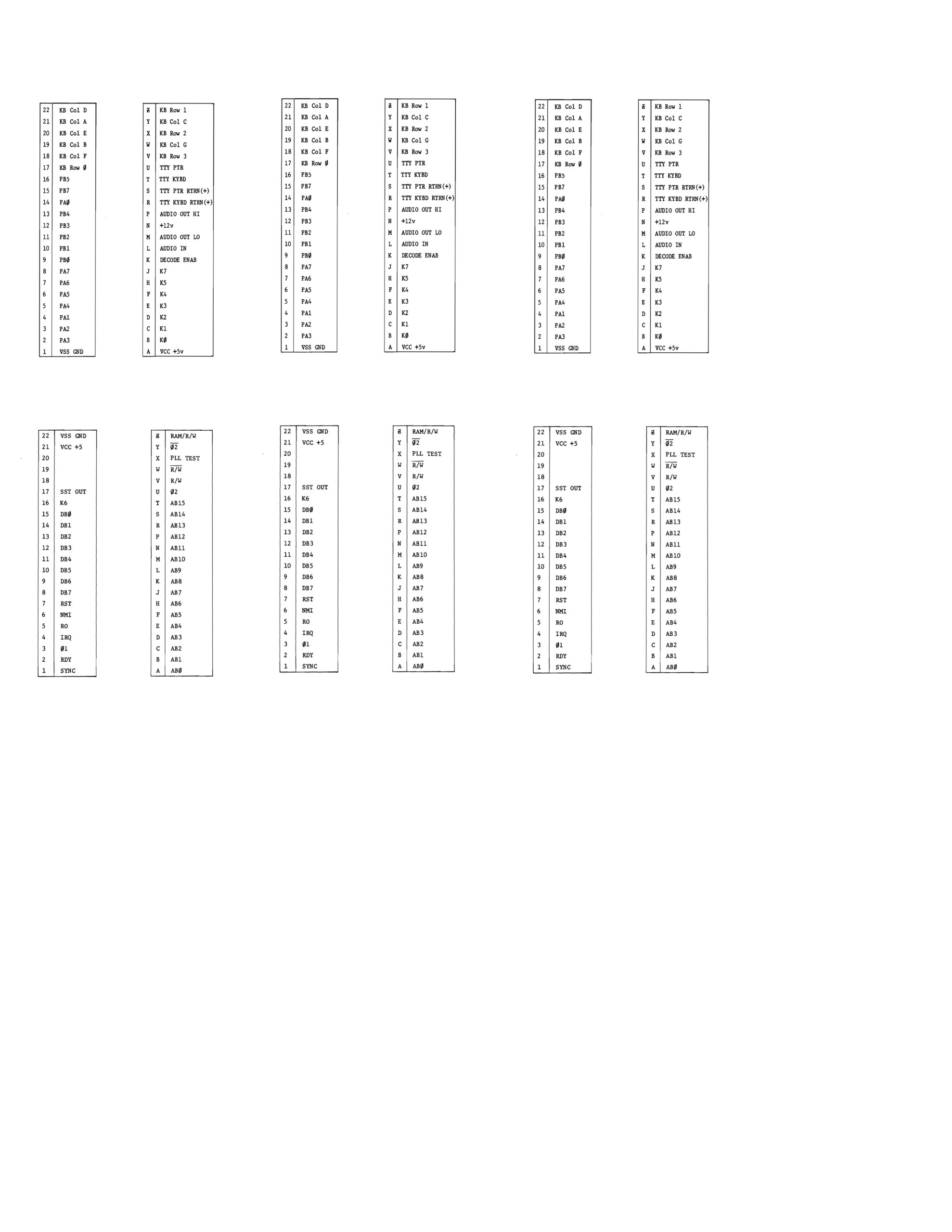
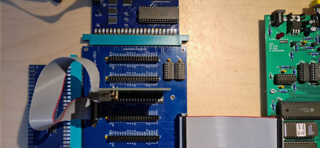
KIM-1 Expansion connector
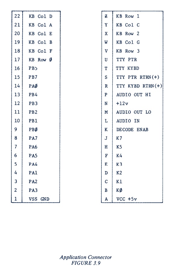
KIM-1 Application connector
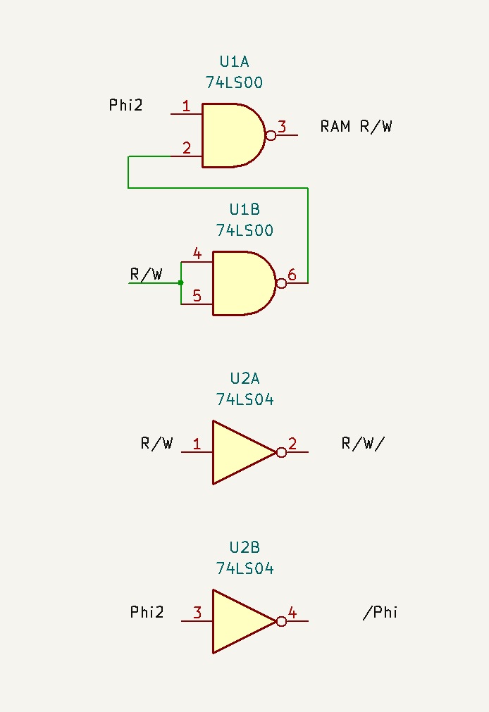
The circuit on the PAL-1 Motherboard Expansion