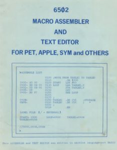
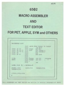
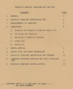
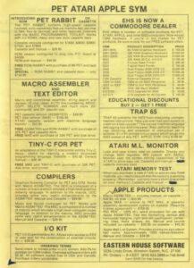
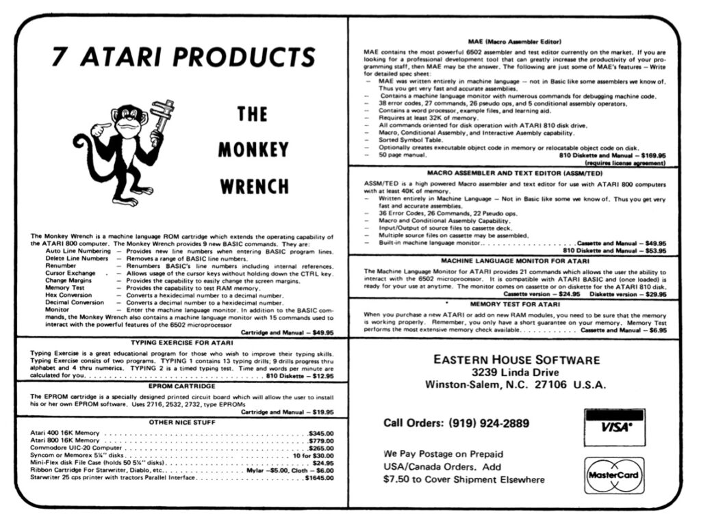
MAE (Macro Assembler Text Editor) or ASSM/TED is a program sold by Eastern House Software for the KIM-1, Apple, PET, C64 and more 6502 based machines.
RAE was the name by Synertek for MAE, as ROMs for the SYM-1 which could be installed to add the Resident Assembler/Editor (RAE). Synertek contracted Eastern House Software to port their Macro Assembler/Editor (MAE) into an 8 KB ROM. AS you can see in the reconstructed source, the adaptations were not much more than adding the SYM-1 I/O such as character I/O and tape handling, the essence of MAE stayed as RAE. It was not that popular in the SYM-1 world, even Synertek used internally another assembler, with more MOS Technology compatible syntax.
The author of MAE and RAE, was Carl Moser. MAE was sold in various forms not only for the KIM-1 and SYM-1 but also for other 6502-based computers including Commodore, Atari, KIM, and Apple and in the Netherlands the Elektor Junior. Other forms of MAE included a cross assembler for 6800 and 8085.
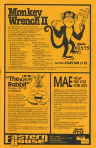
Carl Moser and JR Hall were founders of Eastern House Software, the company that created several products for Atari 8-bit users, including Monkey Wrench and Monkey Wrench II, and the KISS word processor.
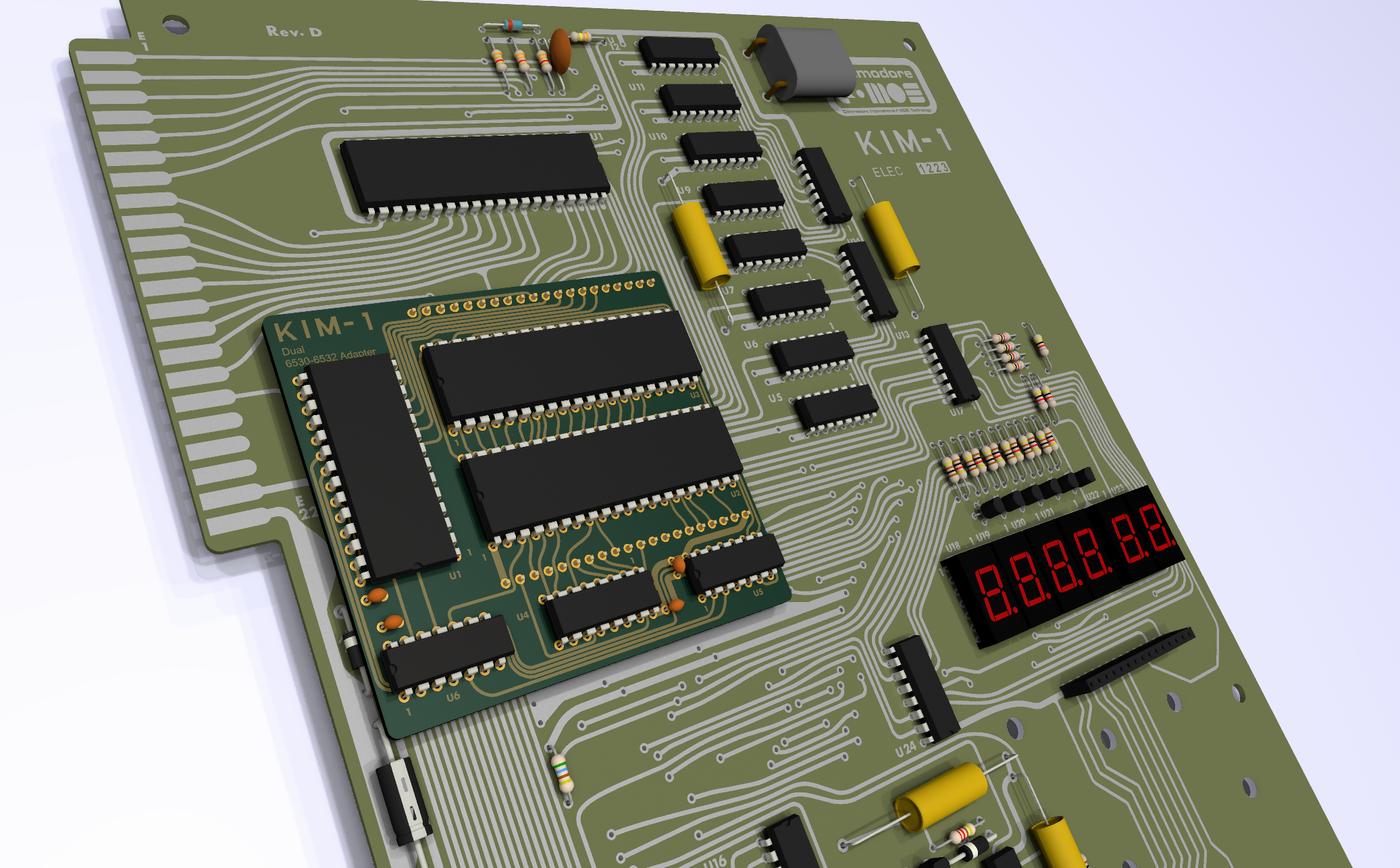
On topic on this site are the preserved KIM-1, SYM-1 and Elektor Junior versions. I have binaries, manuals and (reconstructed) sources for these versions for download.
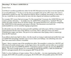
Note that the manuals for the SYM-1 RAE are well written, and a good addition for the manuals of MAE.
On this page:
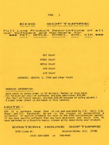
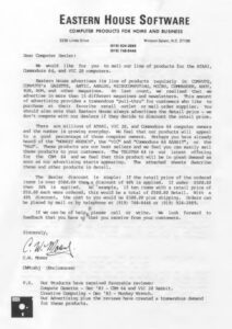
Catalogs and flyers Eastern House Software
PC commandline tools to manipulate MAE/RAE files
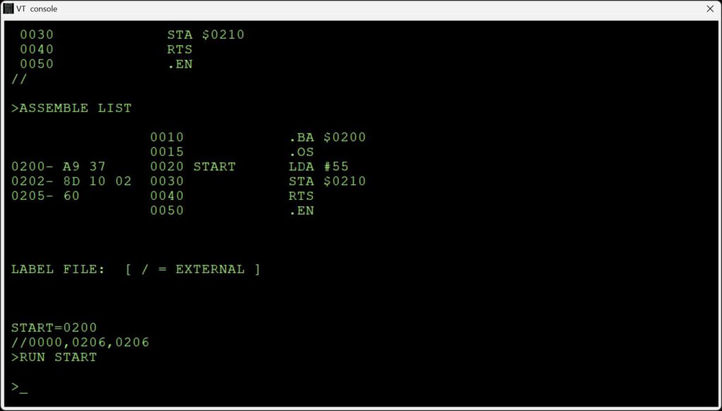
To get text into and out of the ASSM/TED program on the 6502 computer to the PC world,one can use several methods.
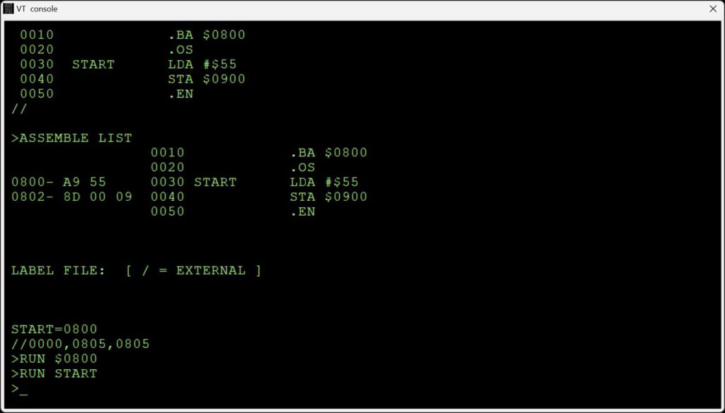
Written in Freepascal. Sources included, can be compiled in Linux etc.
The first method is using a terminal emulator and upload a text file or catch the output of the ASSM/TED program.
That gives some problems, mostly related to missing line numbers, or too much blanks.
Strip Blanks
The output of ASS/TED to the screen contains many blanks. When you want to uplaod the captured output, those blanks have to go
D:\myfiles\MAE\PC tools>StripblanksMoser.exe
V1.0 Strip blanks from captured ASSM/TED Moser source file
V1.0 Hans Otten, 2024
Syntax: StripBlanksMoser <sourcefile with blanks> <output source file to upload
to ASSM/TED> [Y]
Y to overwrite outputfile without question asked
Add numbers
When you have a MAE/RAE source file without numbers, you can add those with this utility, increment of 10.
D:\myfiles\MAE\PC tools>AddNumbersMoser.exe
V1.0 Add numbers 0001-9999 to source file to make a ASSM/TED Moser source file
V1.0 Hans Otten, 2024
Add numbers 0001-9999 to ASSM/TED Moser source
AddnumersMoser <sourcefile without numbers> <output source file with numbers> [Y]
Y to overwrite outputfile without question asked
The other method is to dump or upload the text buffer as memory binary dumps.
Text is stored in memory as:
..
e.g.
the text
10 test
is stored as:
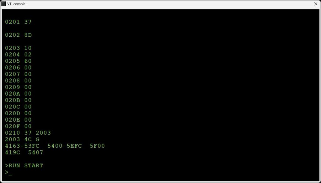
00 10 20 74 65 73 F3
RAE to TXT
Converts a binary MAE/RAE file to an ASCII text file without line numbers and normal line end
D:\myfiles\MAE\PC tools>RAEtoTXT.exe
V1.0 Convert a  ASSM/TED Moser RAE memory dump to text file
V1.0 Hans Otten, 2024
RAEtoTXT sourcefile memorydump output text file  [Y]
Y to overwrite outputfile without question asked
TXT to RAE
Converts a text file to binary RAE format, with line numbers.
D:\myfiles\MAE\PC tools>TXTtoRAE.exe
V1.0 Convert a  text file to ASSM/TED Moser RAE memory dump
V1.0 Hans Otten, 2024
TXTtoRAE <textfile > <output memorydump file  [Y]
Y to overwrite outputfile without question asked
How to dump or upload the the MAE/RAE text buffer
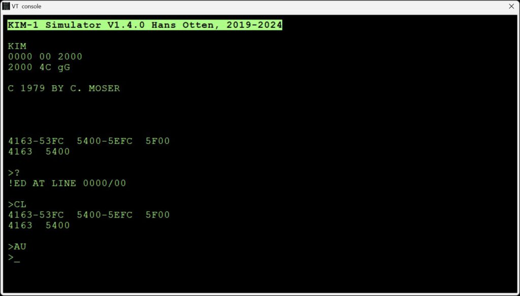
Dump
Start ASS/TED and add some lines
C 1979 BY C. MOSER


4163-53FC  5400-5EFC  5F00
4163  5400

10 test
20 lege regel
set

4163-53FC  5400-5EFC  5F00
4176  5400
Current (4176 in example above is to be stored at D3 (low), D4 (high))
BR to the KIM monitor and save 4163 to 4176 to a file, remember the end address, add that to the filename!
Upload
– Start ASSM/TED and BR to monitor
– Load the text file, place the end address in D3 (low), D4 (high)
– Enter ASSM/TED via the warm start at 2003 (KIM-1) or B003 (SYM-1)