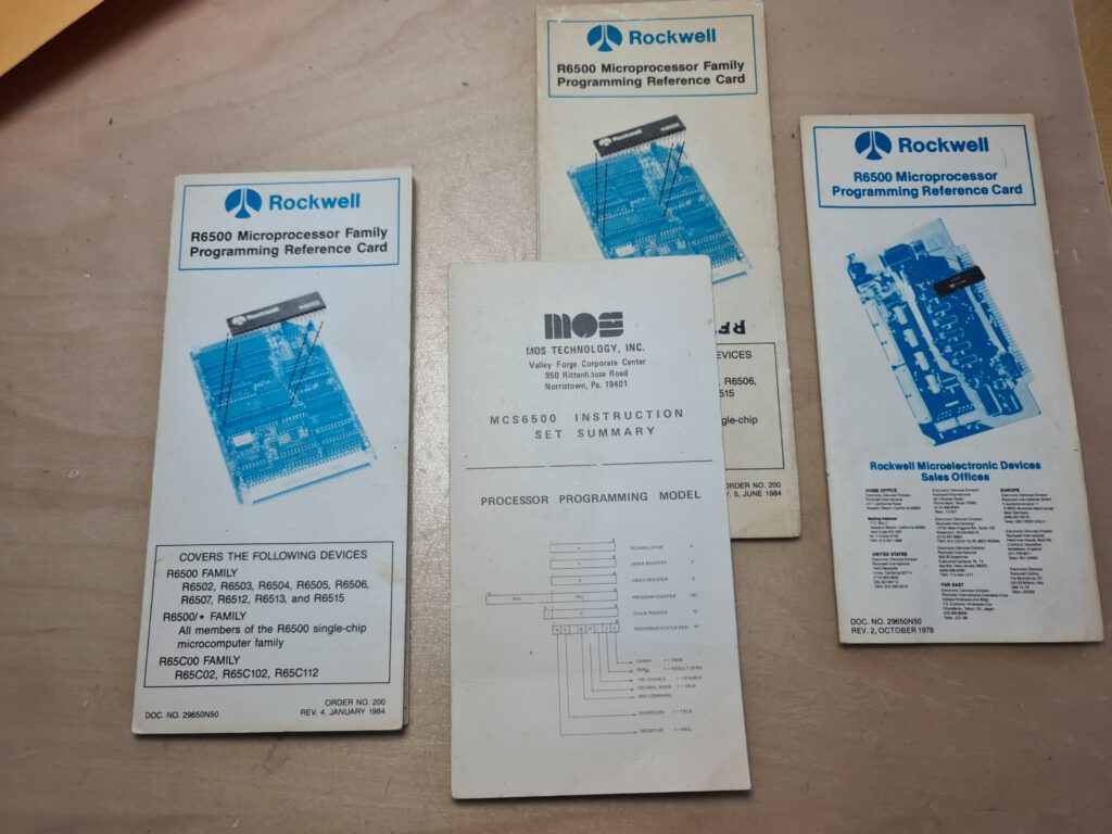
I got hold a about 10 cm of MTU documents. Several I already had in PDF format, some not available yet.
I took the opportunity to scan/rescan/repair what I have online until now.
All documents in the MTU pages are now clean and higher quality, about 50 new PDFs.
Noteworthy are the new revised K-1008 September 1979 document and the now complete and revised K-1013 manuals and 2 versions of the CODOS V1 manual.
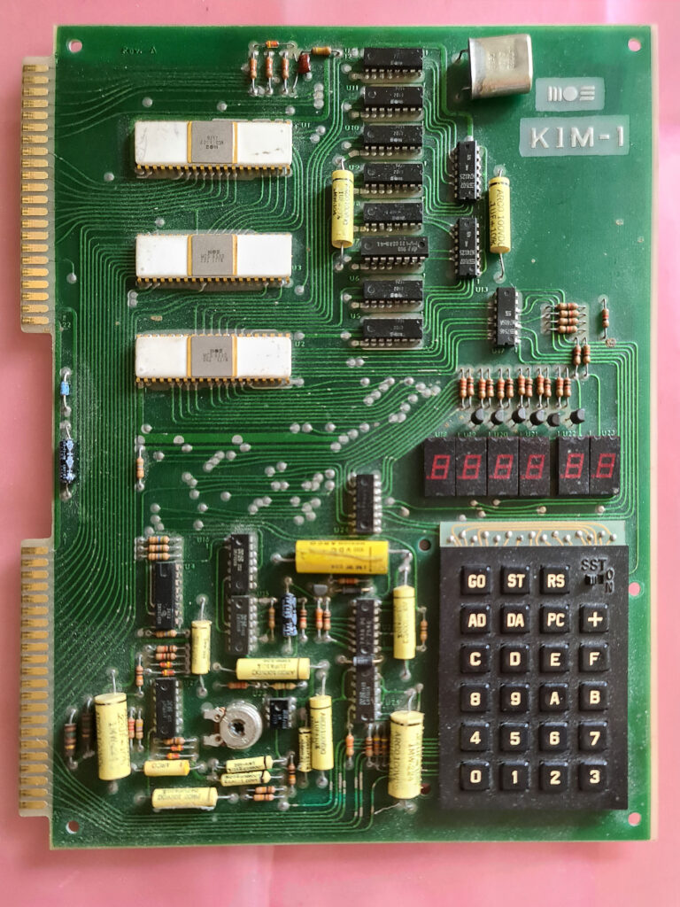
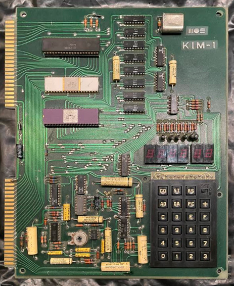
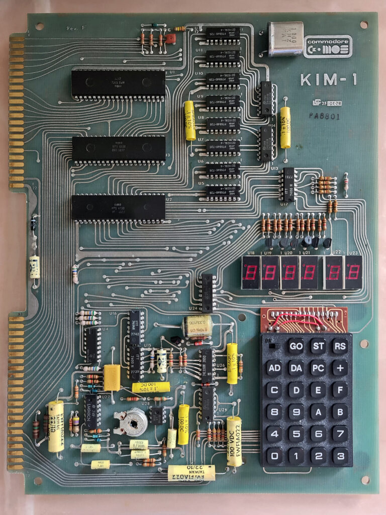
All the K-1002 documents, for KIM-1, SYM-1, AIM 65 and Commodore PET are new.
Micro Technology Unlimited – Retro ComputingMTU history: Hal Chamberlin
MTU Catalogs, Product Descriptions and Newsletters
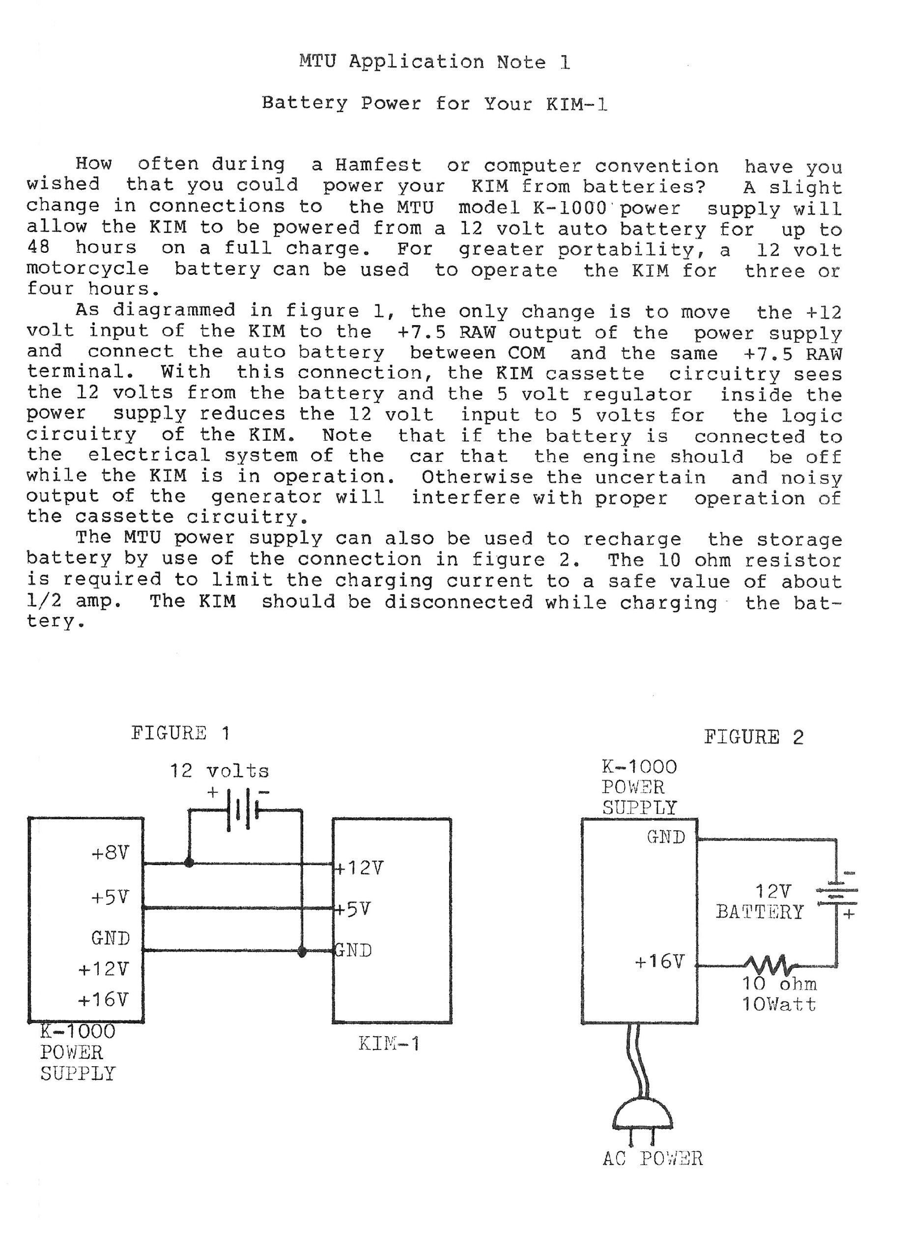
MTU Application notes
MTU K-1000 power unit
MTU K-1002 Audio D/A Converter
MTU K-1005 Card File and Motherboard using KIM/MTU bus
MTU K-1007 PET MTU bus interface
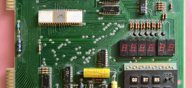
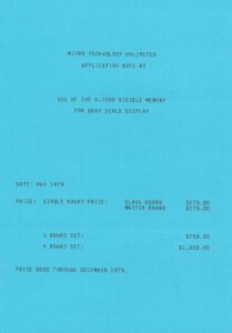
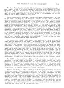
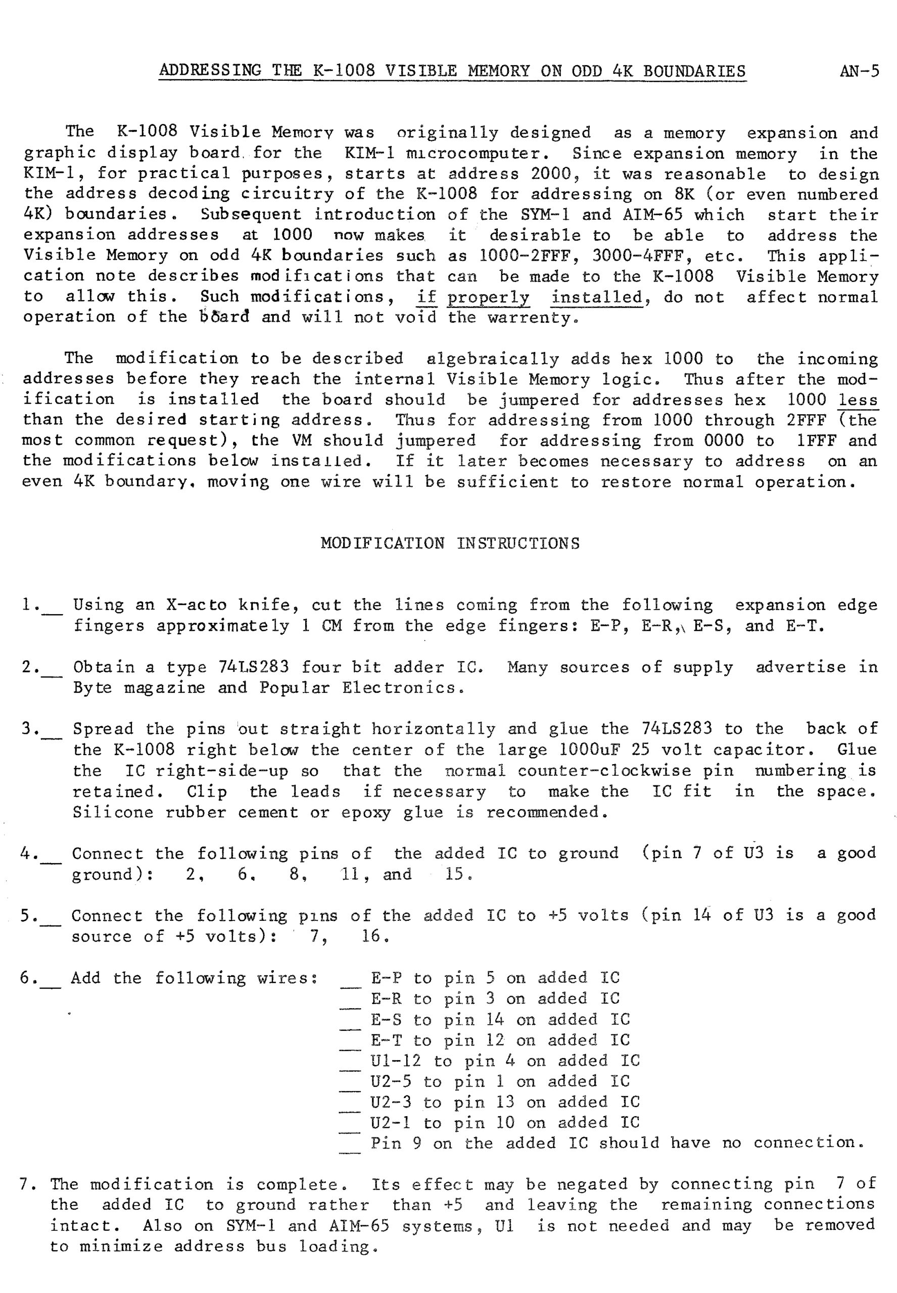
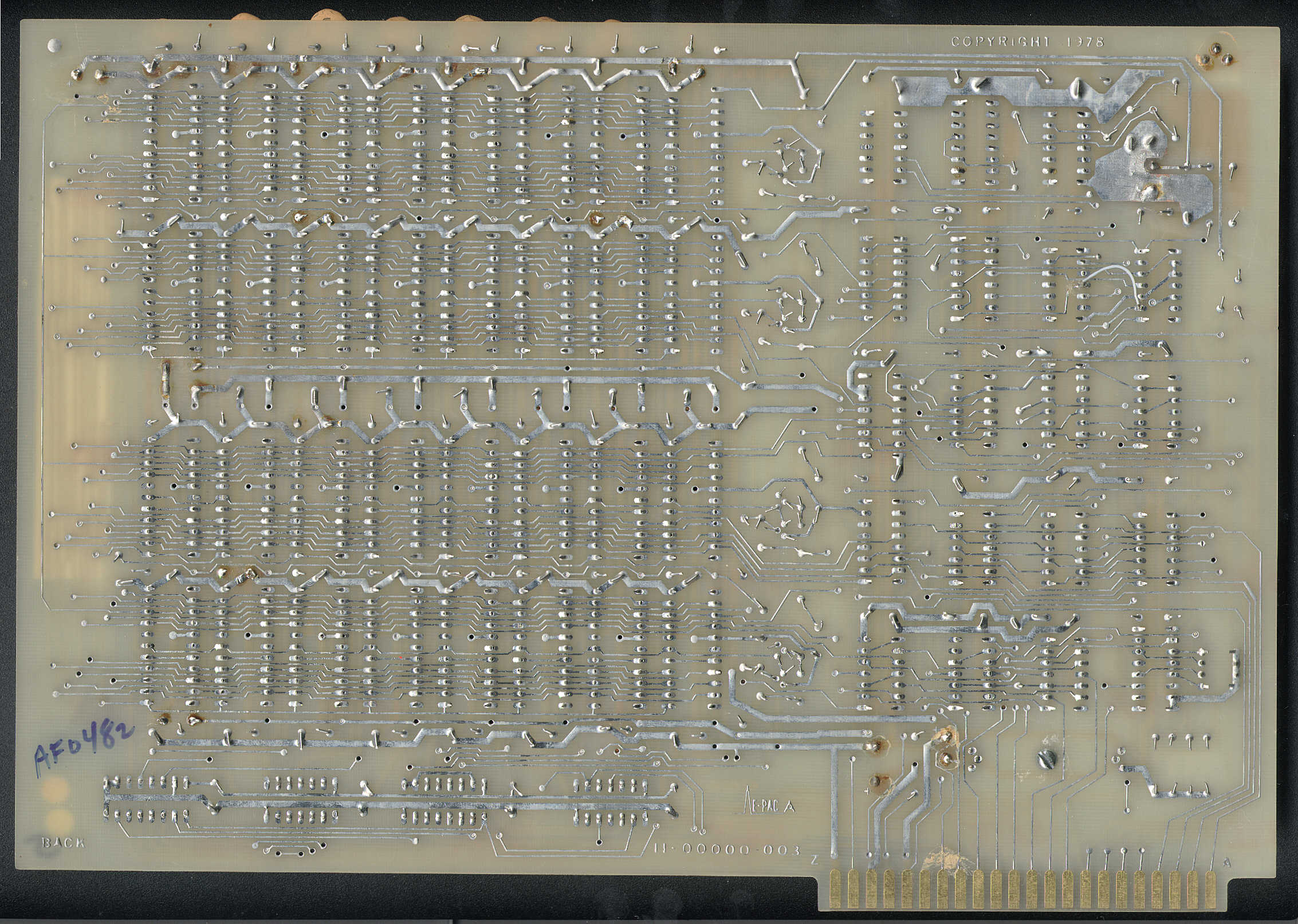
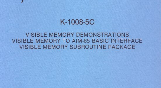
MTU K-1008 Visable Memory
MTU K-1008 documents
Dave Plummer has a K-1008
The K-1008 and the KIM-1 Simulator
Graphics Software Package K-1008
K-1008 Test programs
K-1008-2L Patches to Microsoft BASIC
K-1008 Visable Memory Replica by Eduardo Casino
MTU K-1009-1C AIM 65 Printer Enhancement Package
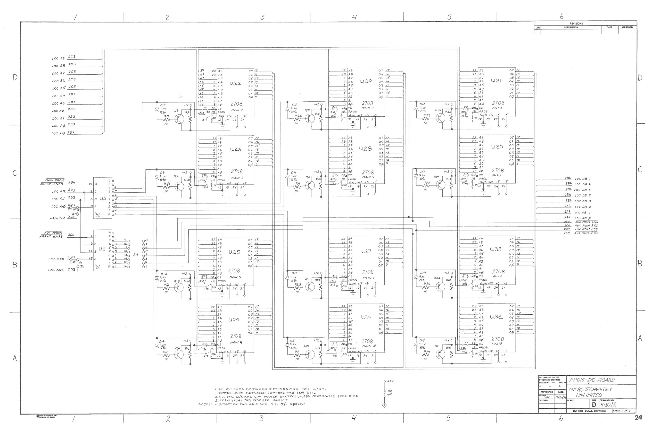
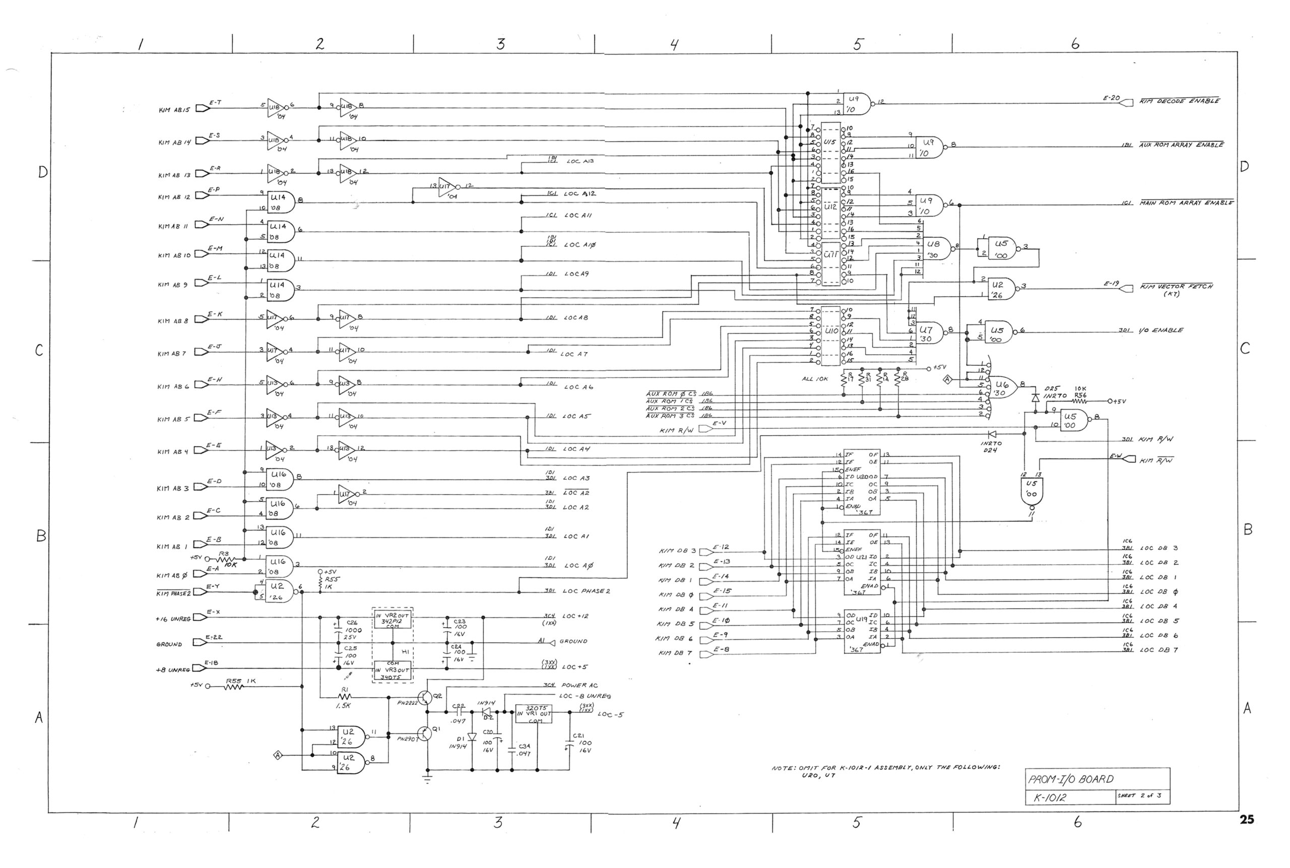
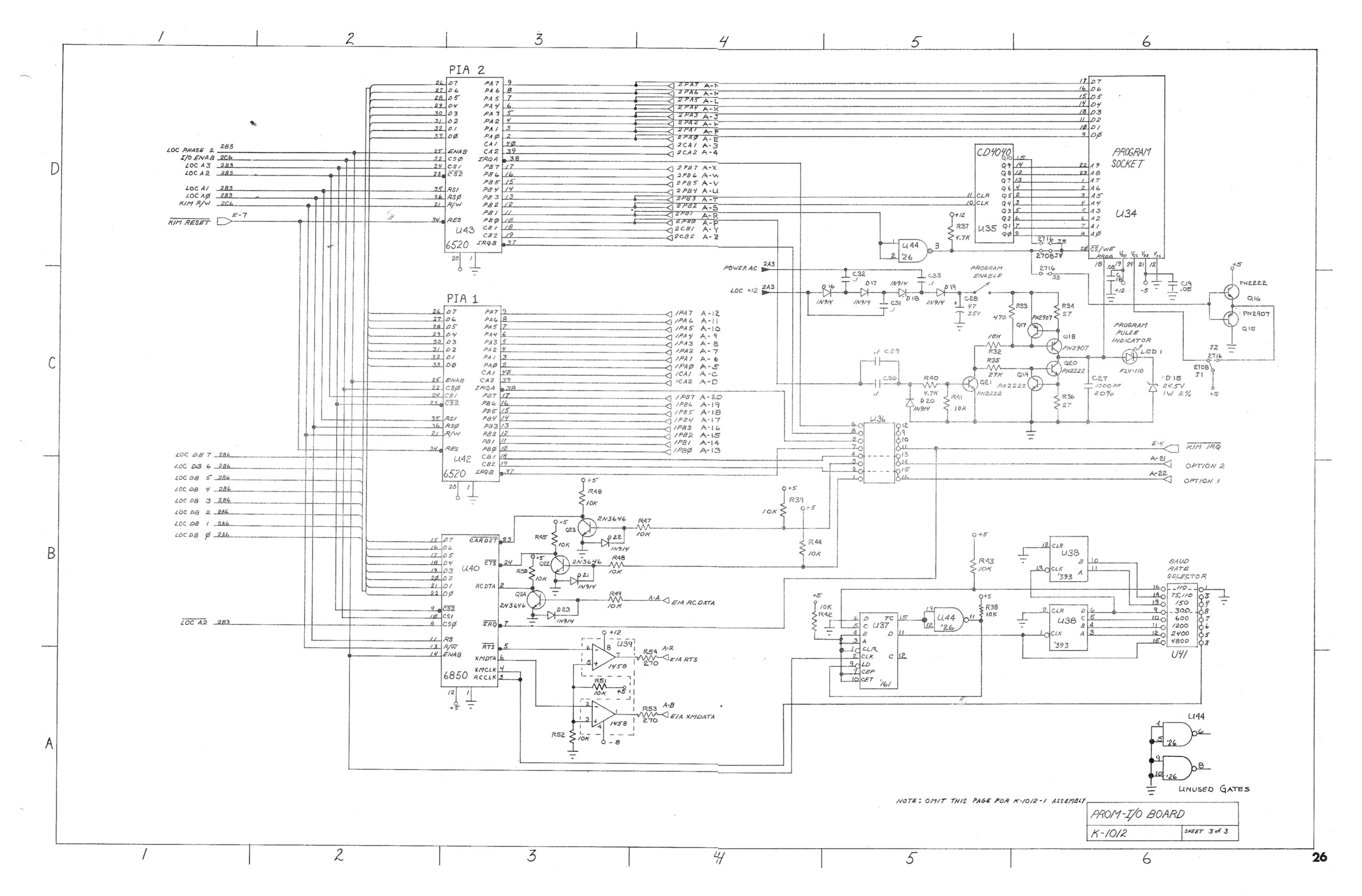
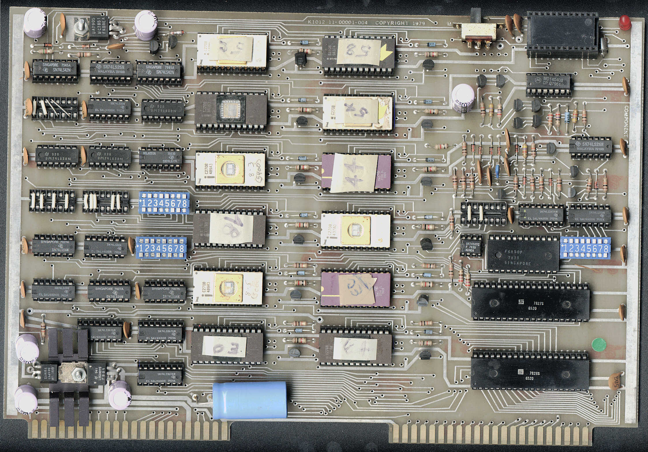
K-1012 PROM expansion board
K-1013 floppy controller
MTU CODOS
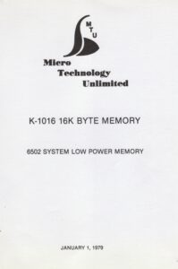
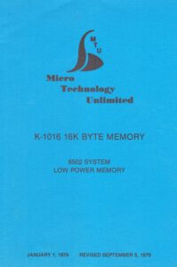
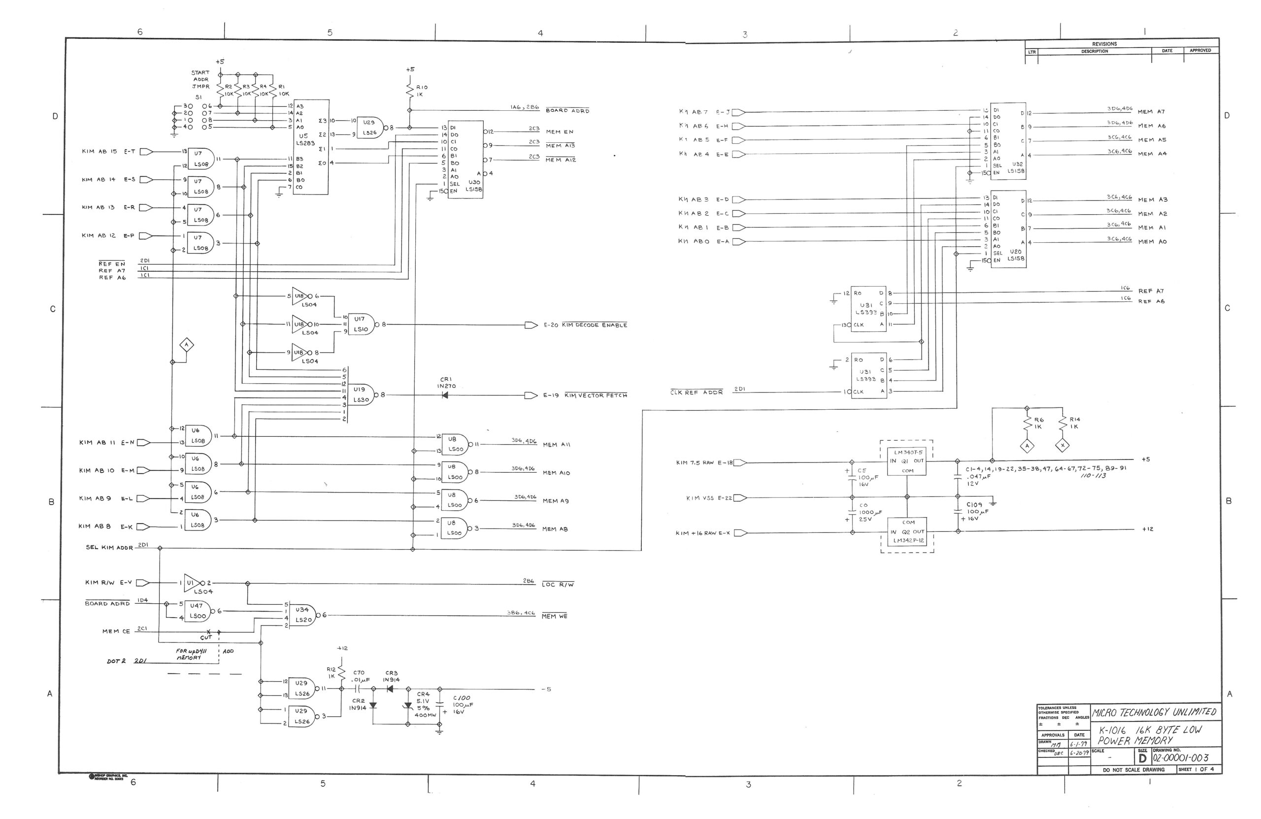
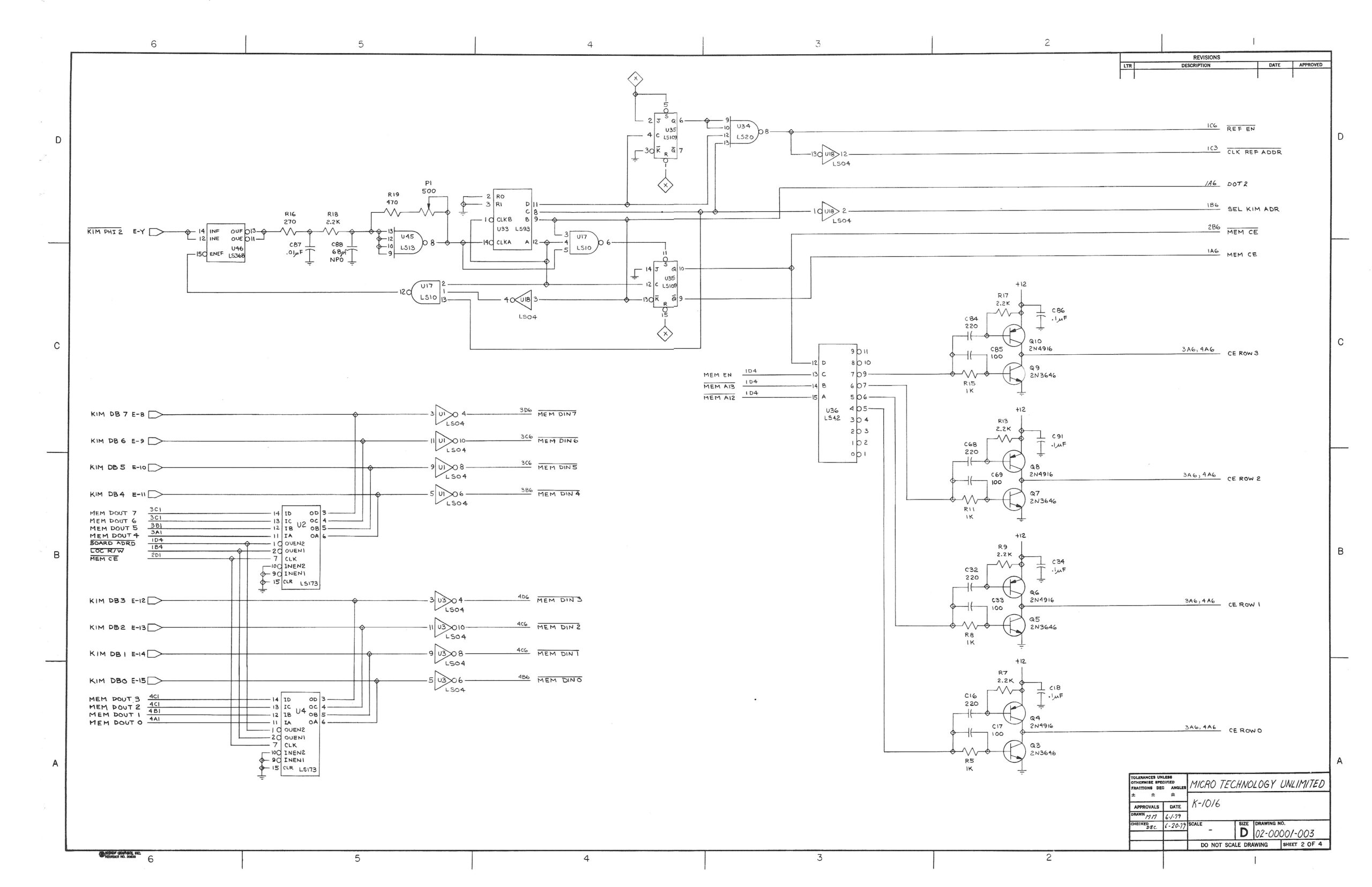
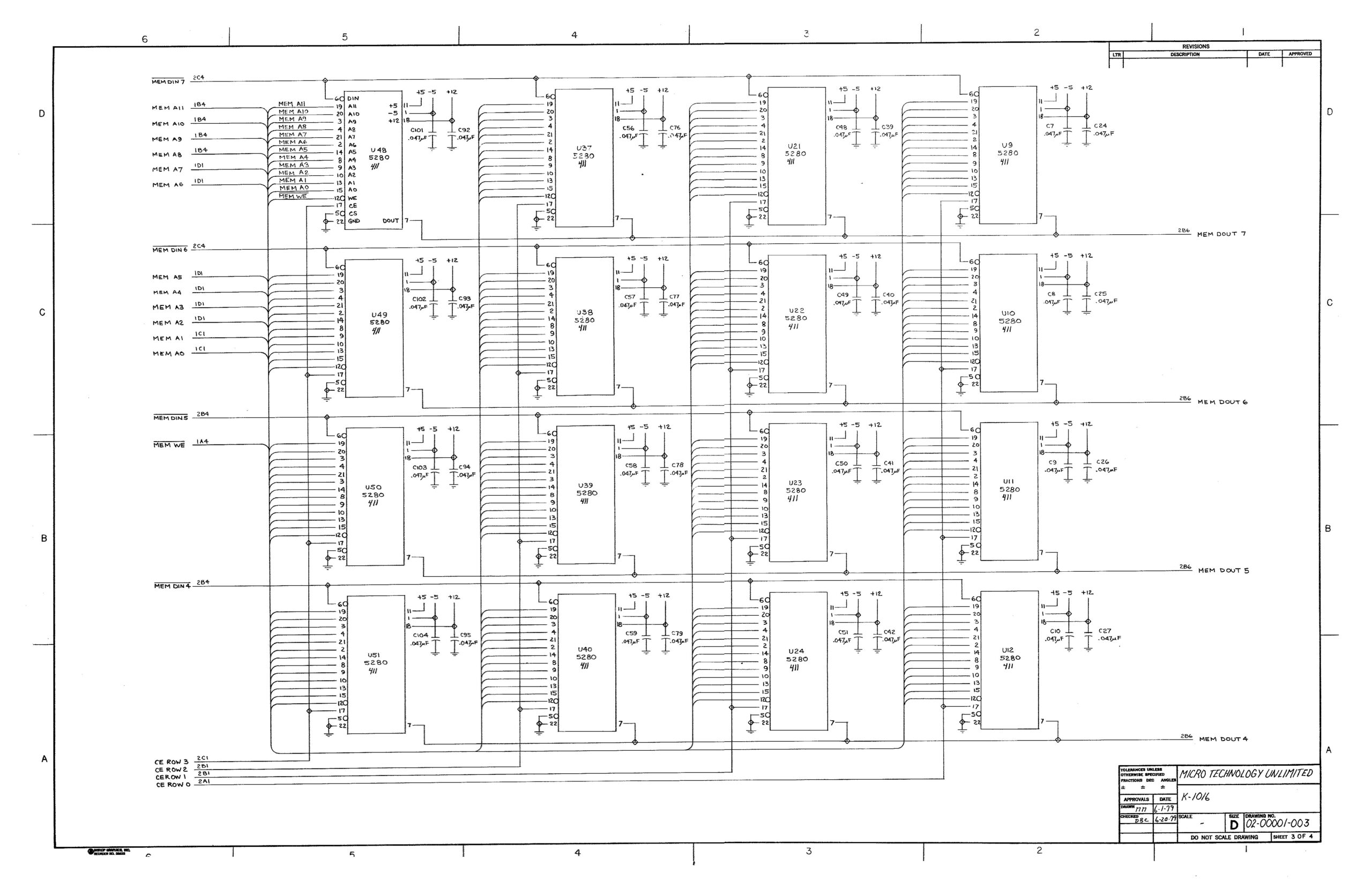
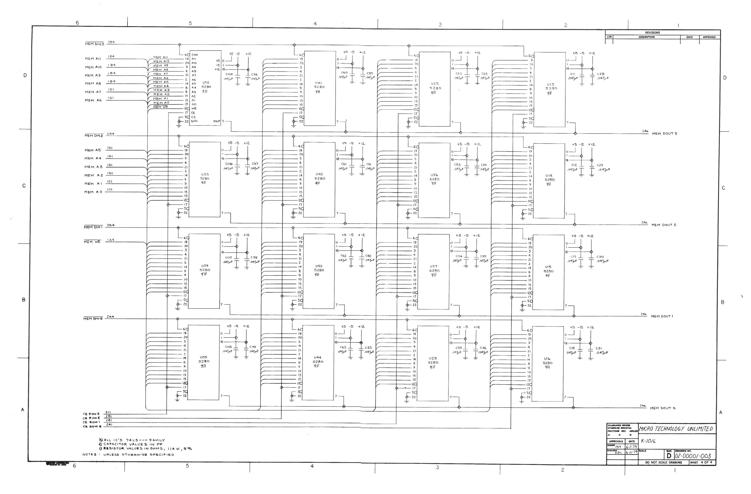
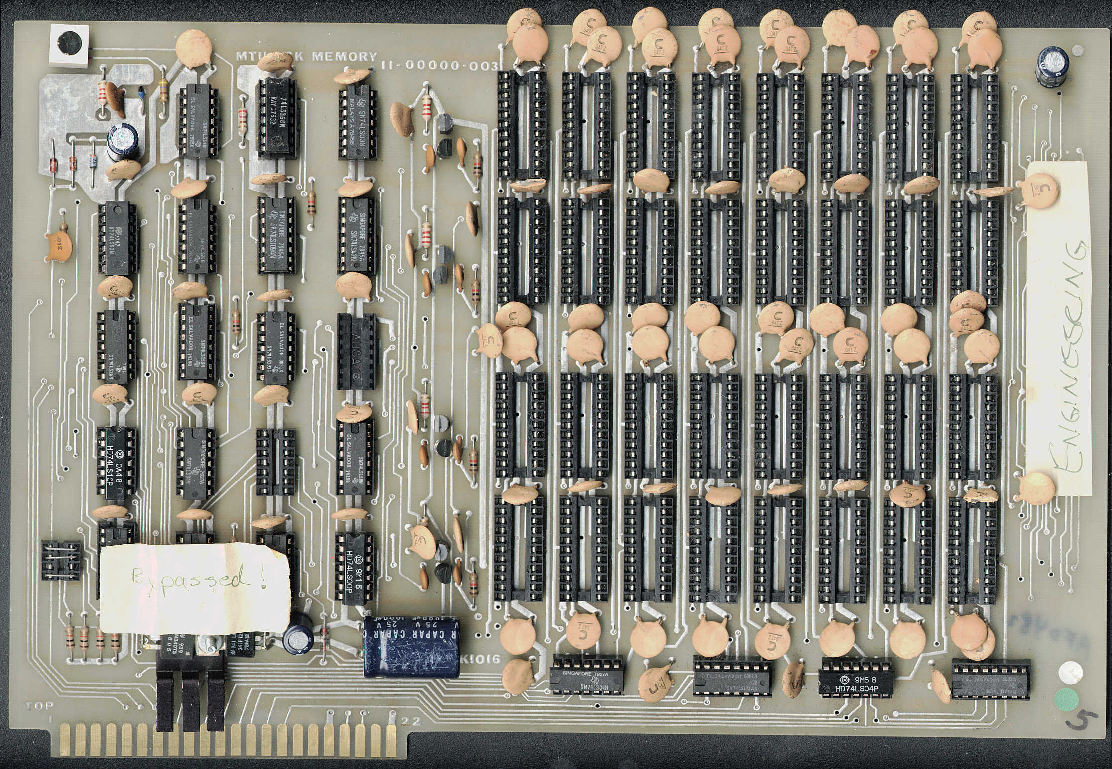
MTU K-1016 16K RAM board
MTU K-1020 Prototyping board
MTU K-1032 Banker RAM ROM I/O