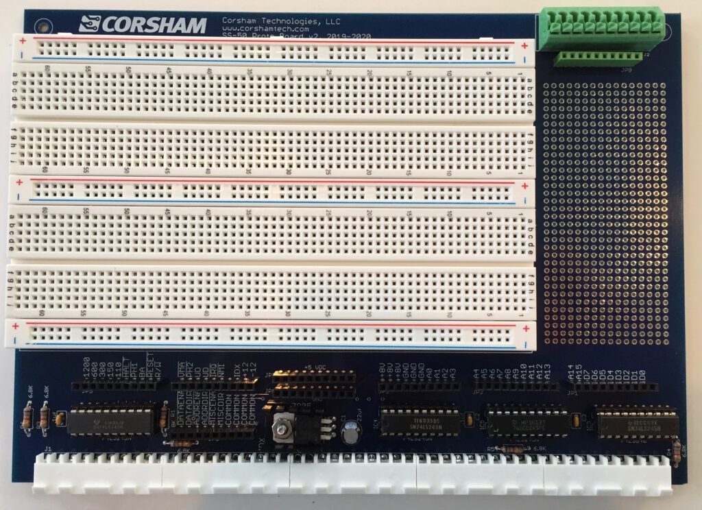
Features include:
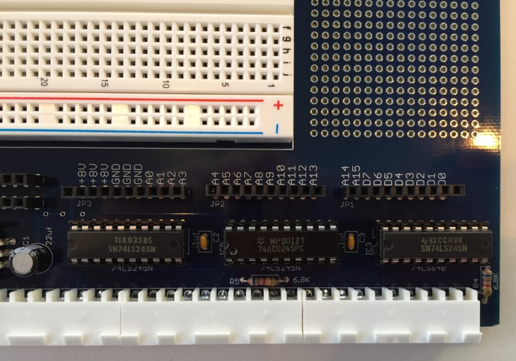
– Large solderless prototyping area. The “tabs” are along the top edge so you can plug in more boards to extend the area.
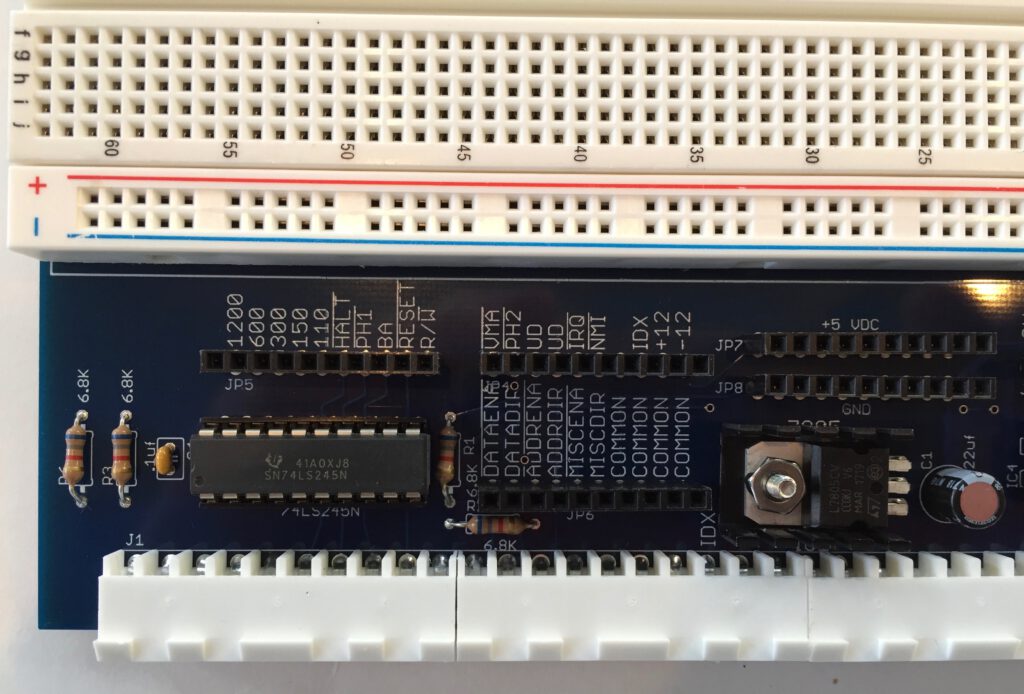
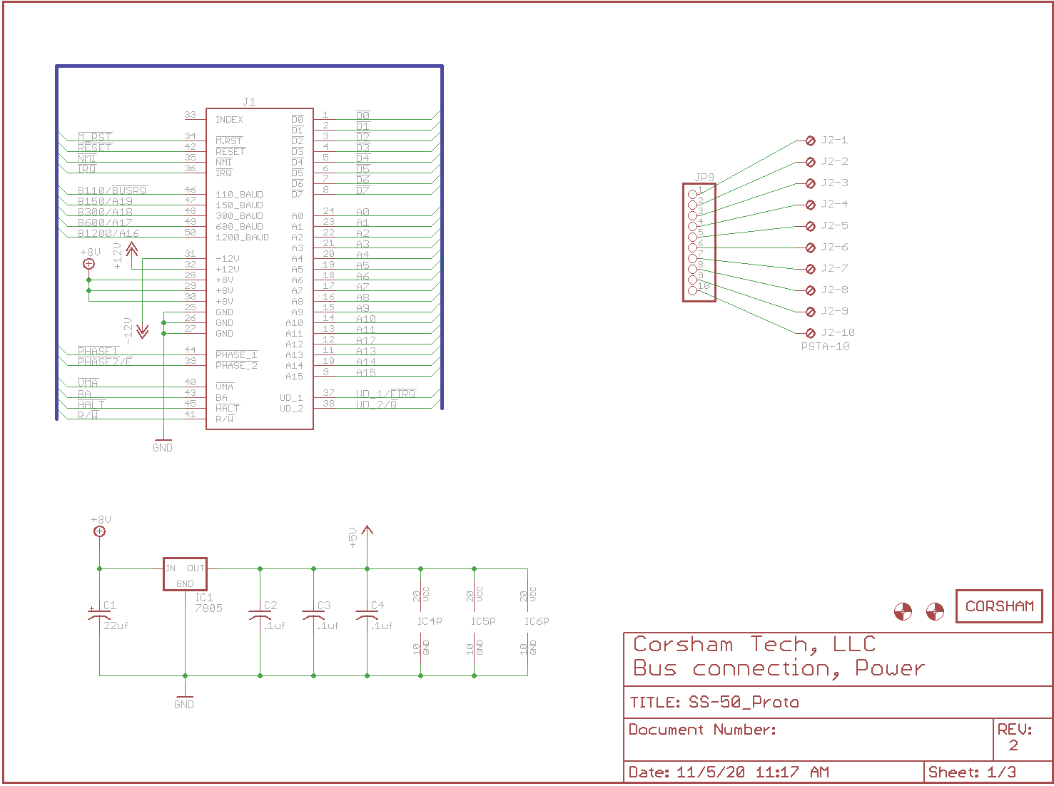
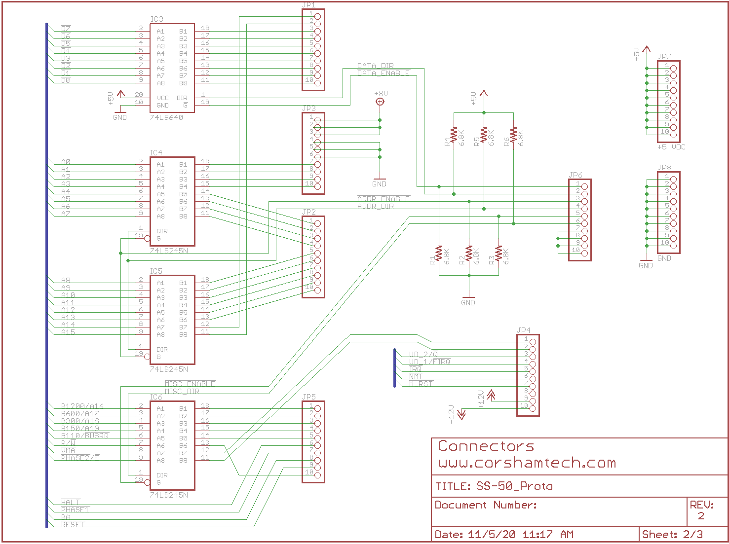
– All main SS-50/SS-50C signals are buffered.
– Buffer direction can be changed by pulling control lines to the proper state.
– 5 VDC power on-board for your circuit; 1.5 amp maximum draw.
– Spring loaded jumper block on upper right corner for connection to external devices.
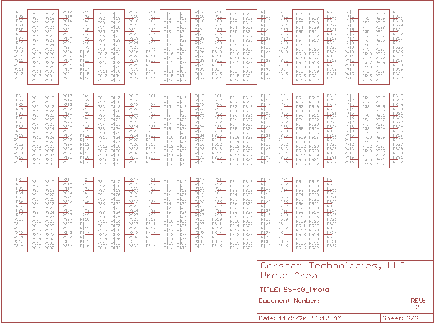
– 16×34 array of plated-through holes for adding other connectors, components, etc.
The bus buffering defaults to taking data from the SS-50 bus and driving to the board, such as for output devices where the CPU is only writing to the board’s circuitry.
However, by pulling one control line low, the data buffers can be reversed for designs that both write and read to/from the board. The address and control line buffers can similarly be controlled so as to drive the bus for those who want to build their own DMA devices or even add a new CPU!
 |
SS-50 Prototyping Manual |
Bus signals are clearly identified: