KIM-3B, a 16K memory module with 2114 SRAM ICs.
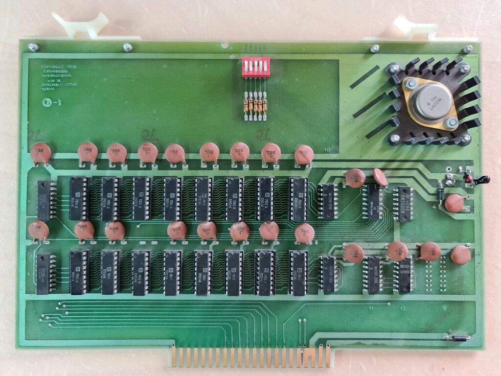
KIM-3B (Stefan Hamann)
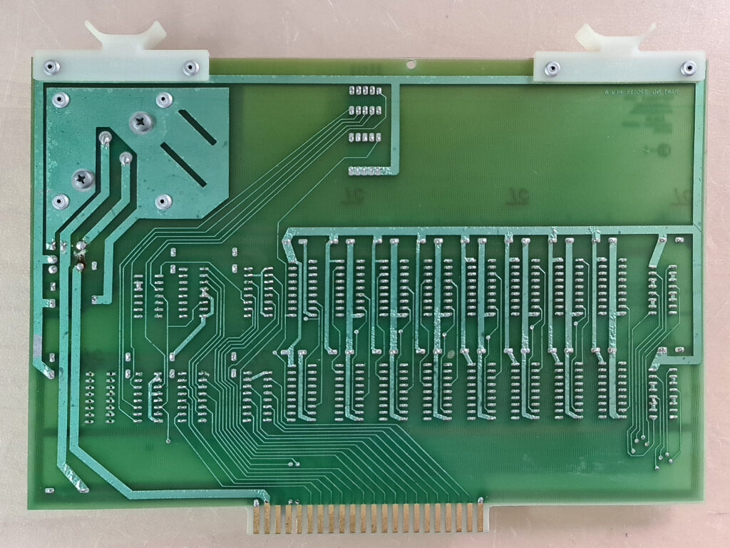
KIM-3B (Stefan Hamann)
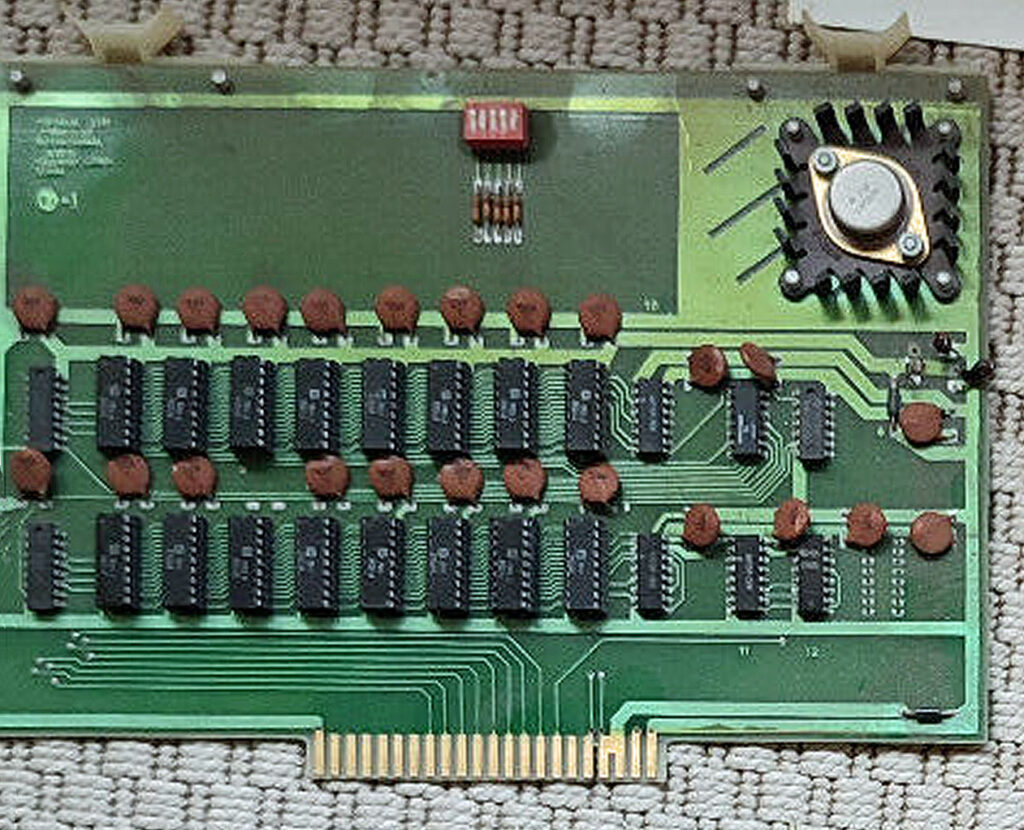
KIM-3B
 |
User’s Manual Memory Expansion Module KIM-3B |
 |
User’s Manual Memory Expansion Module KIM-3B |
About small SBC systems
KIM-3B, a 16K memory module with 2114 SRAM ICs.

KIM-3B (Stefan Hamann)

KIM-3B (Stefan Hamann)

KIM-3B
 |
User’s Manual Memory Expansion Module KIM-3B |
 |
User’s Manual Memory Expansion Module KIM-3B |
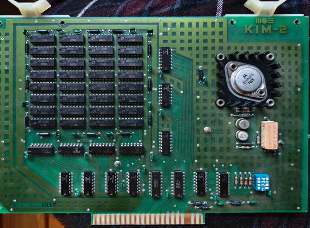
KIM-2 offers 4K RAM with 2102 SRAM ICs. The KIM-3 has 8K RAM, also with 2102 SRAM ICs.
 < <
|
MOS KIM-2-3-4 User Manual Expansion Modules |
KIM-2
On this page:
The KIM-5 Resident Assembler/Editor is a 6502 version of the MOS Technology Cross Assembler. See the pages on the MOS Technology/Commodore assemblers on pagetable.com
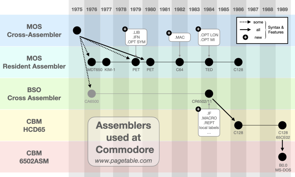
The Resident Assembler was written by Michael Corder (of MOS contractor COMPAS Microsystems) by hand-assembling the Cross-Assembler FORTRAN code to native 6502 assembly.
Consequently, both assemblers were compatible in that they understood the same source format, with the same math features and the same directives and options. That way, they defined the basic format supported by all future Commodore assemblers. This means that the Resident Assembler took uppercase ASCII source files.
John Feagans on the origin of the KIM-5 Resident Assembler/Editor:
As a grad student at Iowa State University, Ames, I had access to all the development of these KIM boards as the local contractor for MOS was Compass Microsystems. The original 6502 assembler was written in Fortran and available on Tymshare. First Michael Corder (aka The Cordless Electric Programmer) hand compiled the Fortran to 6502 assembler. Even the Fortran line numbers were used as labels. This became the basis of the MDT 650, an ICE for 6502, and the KIM assembler. Compass developed another product called the MiniMac–a 6502 development system on a plugin for a DEC PDP-11. I took Corders 6502 assembler and hand translated line by line from 6502 assembler to PDP-11 assembly. When I joined Commodore I ported the assembler one more time to become the PET assembler and later C64 assembler.
In 1977, Commodore announced the Resident Assembler/Editor for the KIM-1, which shipped in the form of the KIM-5 ROM board with three 6540 ROM chips (6 KB total) containing the assembler and a simple editor.
The manuals (see below) from 1977 do not mention the .DBYTE, .PAGE and .SKIP directives. In the source (see below) they seem to be recognized and lead to an error.
The assembler could read source from cassette tape or paper tape, but it could not write OBJ files; instead, it would write the binary to RAM.
If the source was too big to be placed in memory, the assembler could read source files from tape until the .END directive was encountered.
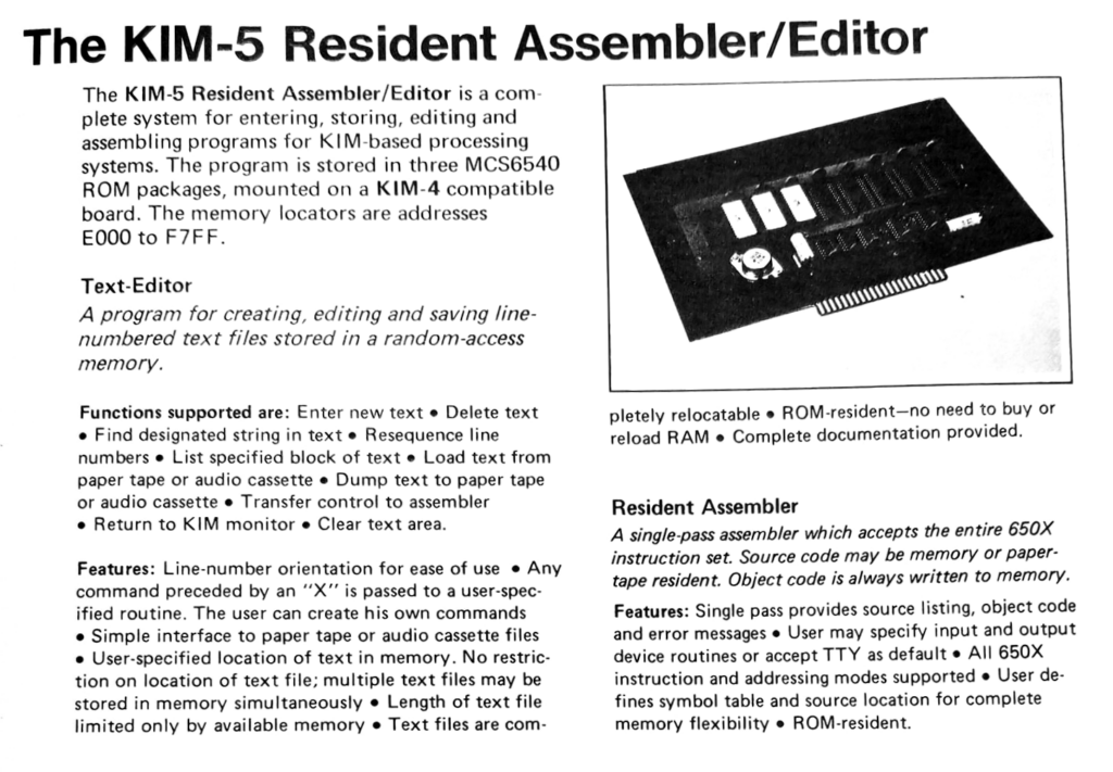
All described in the two manuals that I found:
 |
MOS KIM Assembler Manual Preliminary (KIM-5) |
 |
MOS KIM Text Editor User Manual (KIM-5) |
The KIM-5 Resident Assembler/Editor ROMs
Many years I searched on the internet on fora, websites and friends in the retro world, it did not lead to a dump of the KIM-5 ROMs. It was even doubted the KIM-5 with Assembler/Editor was ever sold, despite the adverts in magazines of that period.
A couple of years ago I saw a listing on ebay.de of a.o. a KIM-5 and a KIM-3B board. I was too late, could not contact the seller or buyer, but I knew the KIM-5 did exist!
A year later Stefan Hamann approached me to ask for information on KIM-1 material he bought from ebay. He was the buyer!
Stefan was so nice to lent me the KIM-5 (and KIM-3B) and the EPROMs he obtained. I have finally a KIM-5 in my hands with ROMs!
The KIM-5 Resident Assembler/Editor is placed in three 2K ROMs of type MOS 6540, and the KIM-5 board configured to show these in memory at E000-E7FF.
With the excellent Backbit Pro Chip Tester I managed to dump the 6540-007, -008, and 009 ROMs. 6540 are strange ROMs, see below. To my surprise the ICs were in excellent condition.
In the other EPROMs (2x 4K 2532) I found a copy of the KIM-5 Resident Assembler/Editor ROMs, nearly identical to the 6540’s. So the dumps are reliable.
ROM dump archives
This archive has the ROM dumps of the KIM-5 Resident Assembler/Editor for KIM-1 Mos Technology Commodore:
With the binaries dumped I have
Source of KIM-5 Resident Assembler/Editor
Recreated source of KIM-5 Resident Assembler/Editor with the aid of TASM32, result is binary identical with the ROM dumps.
Tables, data, jump tables, all recreated. A lot is commented, the editor part needs some attention. Assembles fine.
Eduardo Casino helped me to find the last location dependent statements, and now the program runs at other locations like $9000 after adjusting the .org directive and reassembly.
Eduardo Casino created a CC65 version of the source: Recreated source in CC65 Assembler format of KIM-5 Resident Assembler/Editor
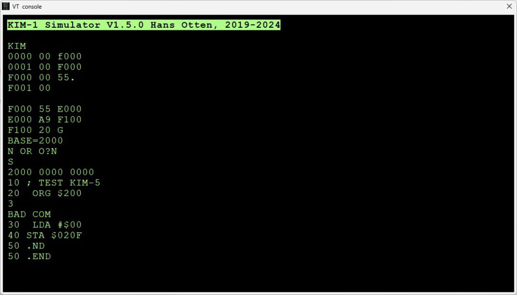
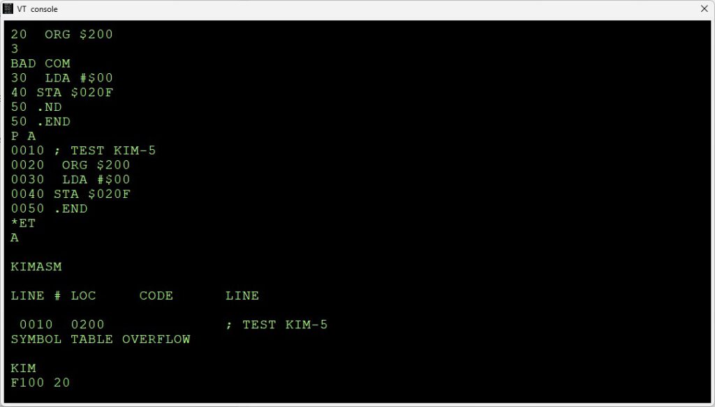
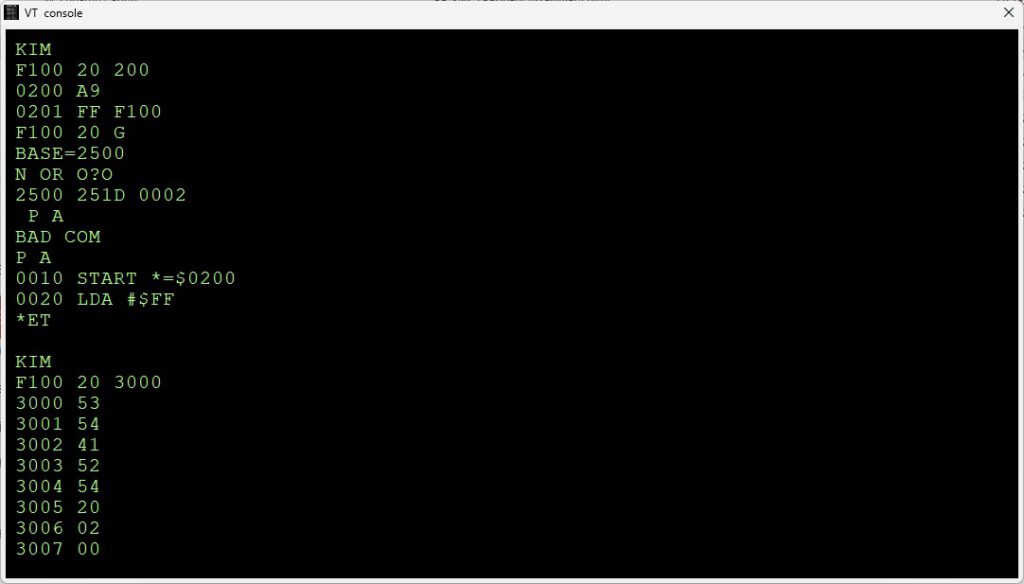
Symbol table at $3000
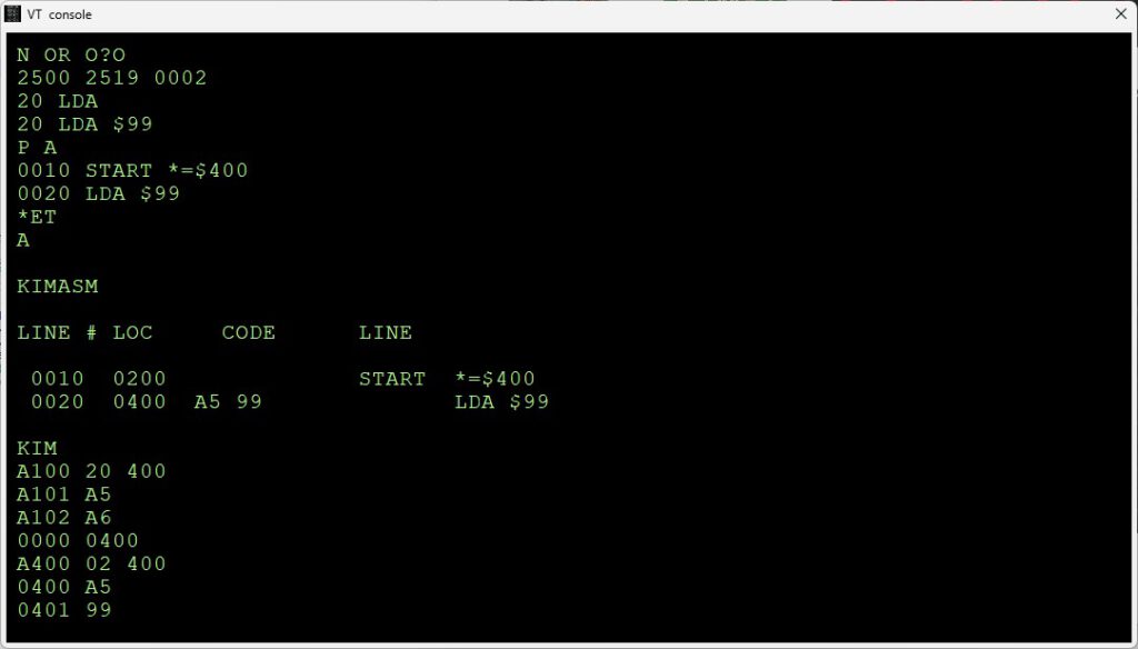
Resident Assembler/Editor at 9000-A7FF
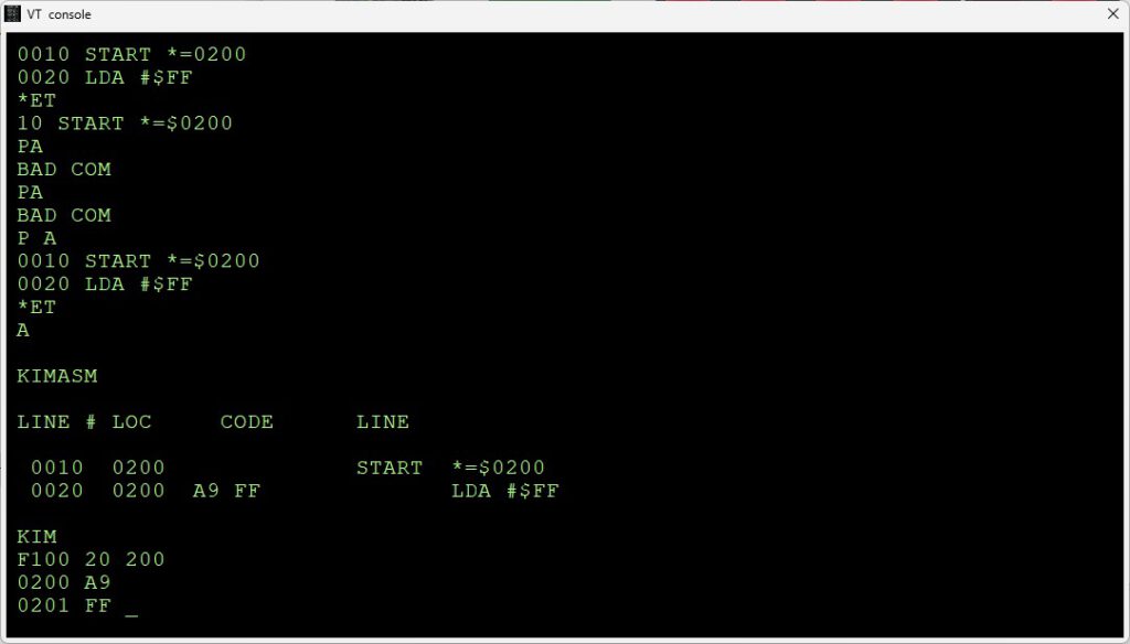
Assembling branch instructions
While working with the assembler Eduardo found weird behaviour by the assembler of the code generated.
Backward branches are done in the usual way. Forward branches generate an extra NOP instruction.
It is not doing any damage, it just wastes space and execution time.
See the next screenshots.
More info and test run at the pages of Eduardo Casino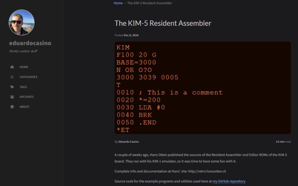
Thanks to Eric Dennison I can show photos of the RNB Enterprises VAK-1 motherboard.
The large motherboard and the huge case with homebuilt 16K static RAM memory card are representative for the KIM-1 systems then!
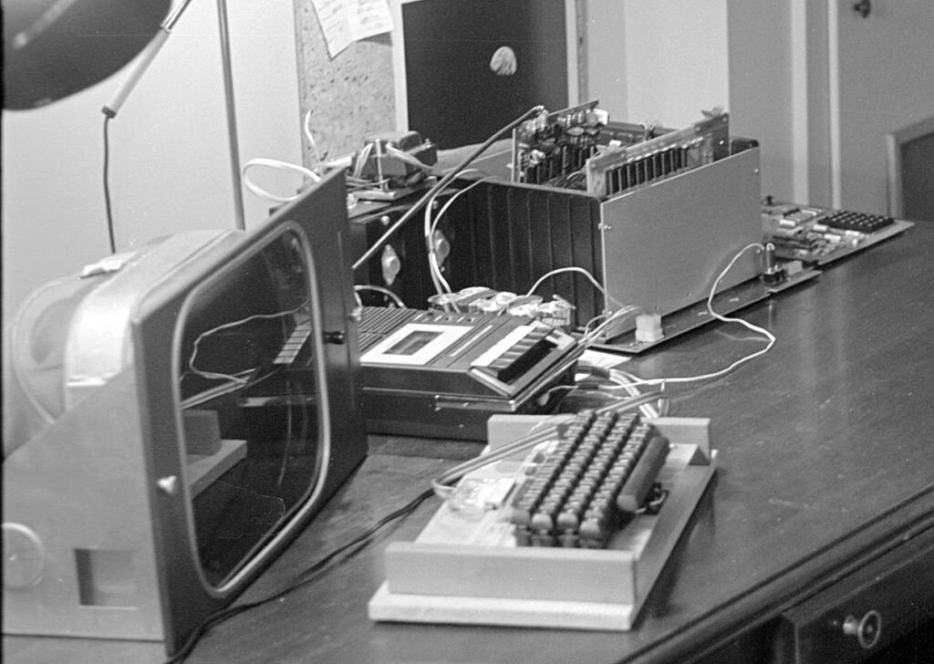
Photo by Eric Dennison
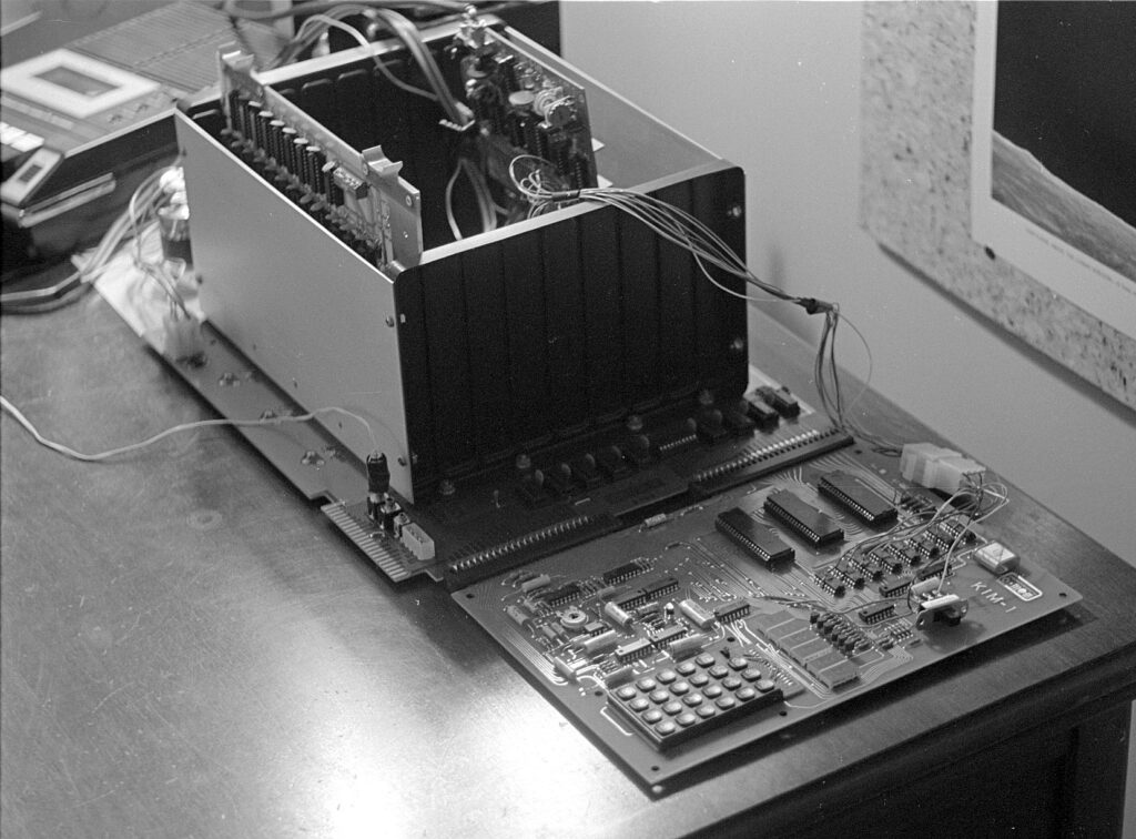
Photo by Eric Dennison
The following text and other files are by (the ‘I’) Alan Cashin.
I am currently looking through old material that has been in storage for many years. I came across a listing of my ‘instant assembler’ written for the basic KIM-1 with 1kB (plus a bit) memory. It was written in about 1979 to help enter assembler programs, saving the task of converting mnemonics to hex code. The tape with it on is long gone, so I coded it for the acme assembler then ran it in your excellent simulator and it works.
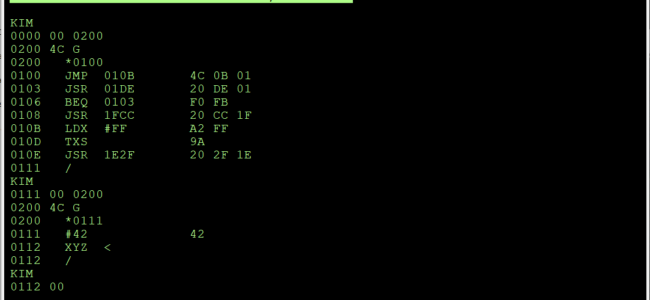
A program by Alan Cashin.
The following text and other files are by (the ‘I’) Alan Cashin.
Here an archive with all sources and binaries and images
I am currently looking through old material that has been in storage for many years. I came across a listing of my ‘instant assembler’ written for the basic KIM-1 with 1kB (plus a bit) memory. It was written in about 1979 to help enter assembler programs, saving the task of converting mnemonics to hex code. The tape with it on is long gone, so I coded it for the acme assembler then ran it in your excellent simulator and it works.
The acme assembler was retrieved from https://web.archive.org/web/20150520143433/https://www.esw-heim.tu-clausthal.de/~marco/smorbrod/acme/ – there is a later version (I believe) in GitHub.
Because there was not much memory, it is small, around 350 bytes (actually smaller as it has an unused block in the middle, which could be the stack if loaded into page 1 or the data bytes if loaded into page 0). It is in 2 parts, a code page around 240 bytes and a set of lookup tables around 100 bytes. It also uses a number of ROM subroutines and it uses the monitor data area as its data area.
It has one failing – no error checking. There was a version that didn’t place the instructions into memory, but passed them to a disassembler. If the original input and the disassembled instruction didn’t match, then it was an error. I don’t have the listing for it.
I’ve included a screen shot run in the emulator. The first entry usually is *<4 hex address>
An instruction is entered as mnemonic (e.g. STA). If it is an immediate (TXS PHP etc) the byte is immediately put in memory. If there are different address modes, the cursor moves to accept the operand, entered as
For conditional branches enter the absolute 4 hex address, it is converted to an offset address
The other possible inputs are:
 / ... return to KIM
 < ... cancel this line (after making a typing error for instance)
 #<2 hex> ... a data byte
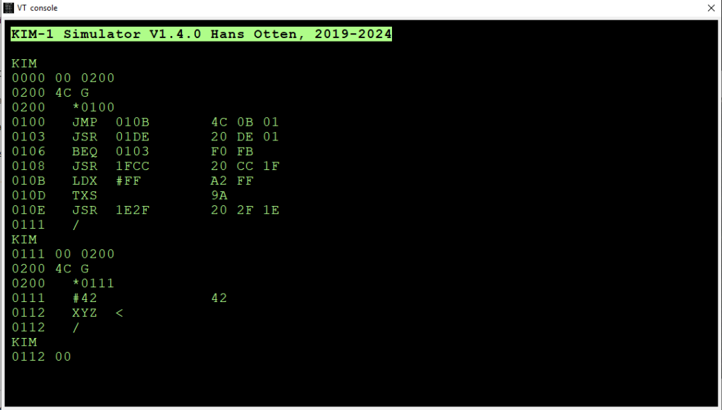
There may be original documentation but I haven’t found it. I also don’t remember how I got the listings as they were created over 40 years ago. As I recall, I wrote the assembler with the code in page 0 and the tables loaded into the 6530 RAM ($1780 – $17E6). This made sense as people didn’t ordinarily put code in page 0. I found part of a printout with the code in page 0, probably done when the assembler was first entered. There’s also a more complete disassembly that includes the tables, written to load at $2000. I don’t know how that happened as the original KIM-1 purchase didn’t have extra memory. But that is the listing I used to create the source. I didn’t own the KIM-1, it was owned by a group. I bought an Ohio Superboard a year later so did most programming with it.
The assembler is now just a curiosity, there are much easier ways of creating 6502 programs. But in those days the first programs (including the instant assembler) were created in several steps:
1. Write the program as if it were for a proper assembler, with labels for data and program locations.
2. Go through the written version allocating addresses to everything (not hard if one counts in hex and knows the length of the instructions)
3. Substitute real addresses for all the labels
4. Work out relative offsets for all the branch instructions (not so easy)
5. Translate all the op codes to hex (tedious)
6. Enter the hex
7. dump the memory to tape
The instant assembler took the information prepared in stage 3 and allowed it to be entered, so saving steps 4,5,6
The assembler uses tables to convert the mnemonic to a binary op code.
1. Each character of the mnemonic is used to access the character table (25 bytes as Z is not used). Each byte in the table has three components, 2 bits, 3 bits, 3 bits – |cc|aaa|bbb| for the mnemonic abc – these are used to create an index into a second table – the index is aaa000+bbb+cc which yields a unique number between 0 and 61 for each mnemonic. This took a lot of juggling to make work.
2. The number is used as an index to look up the base op code. Implied instructions can only be one byte (TAX, PHA, etc) so the assembler does not expect an operand and goes directly to output the op code
3. For instructions that have an operand, a second index is required. The operand can only have a limited set of characters – , # ( ) X Y or hex. These are given values:
, -> 0 (can be left out)
# or a hex digit -> 1
( -> 2
) or X -> 3
Y -> 4
By adding up the value for each part of the operand, a unique index is created. hh=2; #hh=3; hhhh=4; hh,X=5; hh,Y=6; hhhh,X=7; hhhh,Y=8; (hhhh)=9; (hh,X)=10; (hh),Y=11
Some instructions can have an operand or not (eg ROL). If there is no operand, the index is 0.
There are exceptions so there is more manipulation to get the final index. The index is used to look up a modifier to the base op code to get the final op code.
4. The bytes placed into memory for most instructions are (2+hex digits input)/2. Relative branches are modified. If a data byte is input (using #hh) it is treated like an implied op code.
Also, I have tested the idea of writing the assembler in its own format – the assembler can assemble itself (overwriting itself as it runs). This is using the facility for console input from a file.
I’ve now gone through the source (for the acme cross assembler) and put in a lot more documentation. The cross assembler source could be set up to locate the binary anywhere. For no particular reason it is set up to load at 0x0200.
A simple “Hello World” that can be input to the console after 0200 G – assembles then runs it at 0100
*0100 JSR1E2F LDX#0C LDA0110,X JSR1EA0 DEXBNE0102 JMP1C16 #21#64#6C#72#6F#57#20#6F#6C#6C#65#48/0100 G
The source of the Instant assembler (included in the archive above):
		*= $0200		; set program counter
		!to "org0200.o", plain	; set output file and format
; define some KIM-1 ROM addresses
	open = $1fcc
	crlf = $1e2f
	prtpnt = $1e1e
	outsp = $1e9e
	getch = $1e5a
	getbyt = $1f9d
	prtbyt	= $1e3b
	incpt = $1f63
	pack = $1fac
	gokim = $1c16


	jmp	x200b	; convenience, start address same as load point
x2003	jsr	x20de	; gets a character and calls pack
x2006	beq	x2003	; A=0 it was a hex character, try for another
	jsr	open	; not a hex character, set current location to INL,INH
x200b	ldx	#$ff	; set the stack empty
	txs
	jsr	crlf	; CR LF print the current location and 3 spaces
	jsr	prtpnt
	ldx	#$03
	jsr	x20e6
	stx	$f5	; x=0 on return, initial instruction length
	ldx	#$03
	stx	$f6
x201f	jsr	x20d6	; get a character
	cmp	#'/'
	bne	x2029
	jmp	gokim	; if /, return to monitor
x2029	cmp	#'*'
	beq	x2006	; if *, get a new location
	cmp	#'#'
	bne	x2037	; if #, a data byte
	jsr	getbyt
	jmp	x20a5
; assume it's an instruction - get 3 letters
x2037	tay
	lda	x2100-$41,y ; lookup pattern for character
	and	x215f-1,x ; apply mask for 1st,2nd or 3rd character of mnemonic
	sta	$f6,x ; save
	dex
	bne	x201f
	asl	; a - got 3 characters, create index into instructions
	rol	; a
	rol	; a
	adc	$f8
	adc	$f9
	tax
	lda	x2119,x ; get the basic instruction code
	sta	$f7
	ldx	#$02
	and	#$05 ; work out what type
	lsr	; a
	sta	$f4 ; instruction modifier lookup
	sta	$f5
	bne	*+4
	bcs	x209f ; an immediate - go to output
	pha
	jsr	x20e6
x2061	jsr	x20de
	bne	*+4
	inc	$f5 ; final instruction length
	ldx	#$07
x206a	cmp	x2157,x ; possible operand components (X, Y, brackets etc)
	bne	x2077
	txa
	lsr	; a
	adc	$f4 ; add to modifier lookup
	sta	$f4
	bne	x2061 ; if a legal component was found, get more
x2077	dex
	bpl	x206a ; didn't match, try the next one
	pla
	bne	x2087
; convert absolute to relative address for branches
	lda	$f8
	sec
	sbc	#$02
	sec
	sbc	$fa
	sta	$f8
; some instructions are not consistent - special processing
x2087	ldx	$f4
	lda	$f7
	cmp	#$34
	bne	*+4
	ldx	#$0d
	and	#$08
	beq	x20a0
	cpx	#$0a
	beq	x209f
	cpx	#$05
	bne	x20a0
	dex
	dex
x209f	dex
; modify base code according to address mode
x20a0	eor	x20c8-1,x
	eor	$f7
x20a5	sta	$f7
	lda	$f6
	eor	#$0f
	tax
	lsr	$f5
	jsr	x20e6
x20b1	jsr	outsp
	lda	$f7,x
	jsr	prtbyt
	ldy	#$00
	sta	($fa),y
	jsr	incpt
	inx
	cpx	$f5
	bmi	x20b1
x20c5	jmp	x200b
;
; op code adjustment table
x20c8	!8 $01, $04, $0c, $00, $0c, $08, $10, $10
	!8 $18, $1c, $28, $04, $14, $00

x20d6	jsr	getch
	cmp	#'<'
	beq	x20c5
	rts
x20de	inc	$f6
	jsr	x20d6
	jmp	pack
x20e6	inc	$f6
	jsr	outsp
	dex
	bne	x20e6
	rts
;
	!fill 17
; character lookup table -
x2100	!byte $32, $4b, $60, $97, $77, $00, $00, $00
	!byte $1e, $00, $40, $1c, $00, $3a, $11, $d6
	!byte $c0, $7e, $ad, $c3, $00, $c3, $00, $80
	!byte $c1
;
; base instruction patterns
x2119	!byte $8b, $99, $9b, $44, $ab, $a9, $34, $bb
	!byte $30, $90, $b0, $d0, $50, $70, $10, $01
	!byte $49, $24, $f0, $09, $69, $00, $05, $29
	!byte $c6, $cb, $89, $e6, $e9, $c9, $46, $a5
	!byte $00, $ae, $ac, $c5, $59, $19, $d9, $b9
	!byte $ec, $cc, $00, $85, $e5, $86, $84, $79
	!byte $39, $f9, $45, $00, $25, $06, $00, $00
	!byte $65, $26, $66, $41, $eb, $61
; lookup operand characters
x2157	!byte ',', '#', 0, '(', $ff, ')', 'X', 'Y'
; masks used on data retrieved from character lookup
x215f	!byte $c0, $07, $38
I’ve included a scan of 1 page, the handwritten notes were made a long time ago. I think I was trying to figure the total bytes used including the monitor routines. Is it the smallest 6502 assembler written?
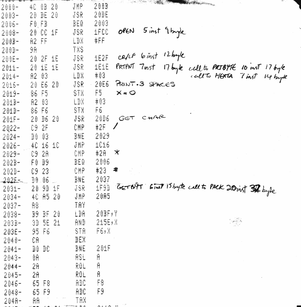
Downloads:
KIM Programs
– Farmer Brown
– Lunar Lander
– Sample extension for XKIM
;=====================================================
; A sample extension for the Extended KIM monitor.
; This is a very simple example of how to write an
; extension (adding a new command) for the
; Extended KIM monitor.
;
; How can you test this? Easy. First, use the “?”
; command in the extended monitor and verify the
; “Z” command is not listed, then load the binary
; version of this file. Do “?” again and you’ll see
; the new command has been added and can be used.
;***********************************************************
; This memory test was originally based on Jim Butterfield’s
; memory test program in the First Book of Kim, but has
; grown a bit.
;
; This now tests every memory location using a rolling 9-bit
; pattern. Ie the pattern repeats every 9 bytes, so this
; will detect most shorted address line problems. I use
; this to test memory boards, so it will run forever unless
; an error is detected. At the end of each pass, a ‘.’ is
; printed.
;
; This does output to the TTY port, so if you’re only using
; the default KIM display, the output functions will need to
; be tweaked. Not hard to do, but I didn’t need it.
;
; Written February 2006 by Bob Applegate, but it uses some
; bits of code from Jim Butterfield, and Ross Archer
; (http://www.6502.org/source/io/primm.htm).
;
; bob@applegate.org
; www.k2ut.org – look for my KIM page
;
; Rev 1.0 – 02/02/2006
Downloads:
Memory test for the KIM-1
(see also the Microchess page)
Downloads:
The hex file MicroChessOut can be loaded directly into the KIM CLONE and run from $2000
Archive with source.
Following the header "Peter Jennings, www.benlo.com" I was pleasantly surprised to see the website still active:

http://benlo.com/microchess/index.html
http://benlo.com/files/Microchess6502.txt


The source code Microchess6502.txt contains the additional note on line 35:

"; Updated with corrections to earlier OCR errors by Bill Forster, August 2005."

Line 73 comments on the cross-assembler used:

"BMCC    =    $E5         ; was BCC (TASS doesn't like it as a label)"

Looking for information about TASS led me to:

https://www.c64-wiki.com/wiki/Cross_Assembler

Reading from "64Tass/6502Tass: Another native "Turbo Assembler", developed for DOS (6502Tass), later also for Unix, Linux and Windows32 (64Tass)," I suspect the 1996-2002 code by Peter Jennings used the DOS version, but I am running Windows 10 on a modern laptop and I can't find a way to run 16-bit applications without using third party tools like DosBox or an emulator in VirtualBox.

So I decided to try out Tass64.  I found a link to the Windows version on sourceforge, https://sourceforge.net/projects/tass64/.  The documentation is included in the zip file, and also here http://tass64.sourceforge.net/.


Without really reading the documents, I just ran Microchess through the Assembler and got errors.  Below are the errors I got, and how I fixed/hacked/patched each one.

First Attempt:

Error messages:    31
Warning messages:  3
Passes:            2

....Oof.....


Error Group 1:

MicroChessSource:37:8: error: general syntax
    cpu 65c02
        ^
MicroChessSource:38:9: error: general syntax
    page 0,132
         ^

Correction:

Change 37 to: .cpu "65c02"
Change 38 to ; page 0,132

Line 38 is commented out because 'page' "gives an error on page boundary crossing, e.g. for timing sensitive code" and I am simply going to put my faith in Peter Jennings and hope for the best here.

Line 37 can be changed to reflect the CPU you are using.  I got my parts assembled by Bob, and leaving "65c02" as the cpu version works for me on the KIM CLONE.

Error Group 2:

MicroChessSource:729:6: error: general syntax
                db      $2c             ; used to skip over LDA #$20
                        ^
MicroChessSource:859:12: error: general syntax
 Hexdigdata     asc     "0123456789ABCDEF"

Correction:

For all the lines that use "db" or "asc," change the pseudo-op to ".text"


Now I got:
-----------------------------------------------------------------------------
C> 64tass.exe -o MicroChessOut MicroChessSource
64tass Turbo Assembler Macro V1.55.2200
64TASS comes with ABSOLUTELY NO WARRANTY; This is free software, and you
are welcome to redistribute it under certain conditions; See LICENSE!

Assembling file:   MicroChessSource
Error messages:    None
Warning messages:  None
Passes:            2
Memory range:      $1000-$1524   $0525
Memory range:      $1580-$15dc   $005d
-----------------------------------------------------------------------------

I think I'd like to run Microchess from $2000 up in one block, so I will modify line 95 and 869:

Change line 95 to ";*= $1580"
and comment out line 869.

-----------------------------------------------------------------------------
Memory range:      $2000-$2581   $0582
-----------------------------------------------------------------------------

Now the source will assemble, but it won't work yet.  The Peter Jennings code with TTY was written for the "6551 Asynchronous Communications Interface Adapter (ACIA)," not the "standard TTY" routines built into the KIM monitor that we see in the First Book of KIM etc.

http://archive.6502.org/datasheets/mos_6551_acia.pdf
https://en.wikipedia.org/wiki/MOS_Technology_6551

First, I comment out the ACIA addresses from line 42.

;ACIADat    =     $7F70
;ACIASta    =    $7F71
;ACIACmd    =    $7F72
;ACIACtl    =    $7F73

Then, I add in the addresses of the KIM monitor TTY routines for getting (blocking) and outputting 1 character.

; http://www.zimmers.net/cbmpics/cbm/kim1/kim-hints.txt - See "KIM SUBROUTINES"

TTY_GETCH = $1E5A  ; Register States: In to A, X preserved, Y = FF
TTY_OUTCH = $1EA0  ; Register States: X preserved, Y = FF, A = FF

Now, I move to line 822 and start making changes to the I/O Routines.

(1) Comment Out the Init function 825-829, don't need.  I leave the label and rts to allow it to work as a dummy sub routine rather than deleting all references to it in the code.

(2) Replace the meat of "syskin" on 833 with code to push the affected registers, call TTY_GETCH, and restore affected registers.

(3) Replace the meat of "syschout" on 842 to push the affected registers, call TTY_OUTCH, and restore affected registers.

Now the code after line 822 looks like:

;
; 6551 I/O Support Routines
; Replaced with KIM Monitor Routines for KIM Clone - Neil 2020
;
;
Init_6551      ;lda   #$1F               ; 19.2K/8/1
               ;sta   ACIActl            ; control reg
               ;lda   #$0B               ; N parity/echo off/rx int off/ dtr active low
               ;sta   ACIAcmd            ; command reg
               rts                      ; done
;
; input chr from ACIA1 (waiting)
;
syskin         ;lda   ACIASta            ; Serial port status
               ;and   #$08               ; is recvr full
               ;beq   syskin             ; no char to get
               ;Lda   ACIAdat            ; get
               PHY
               JSR TTY_GETCH
               PLY
               RTS                    ;
;
; output to OutPut Port
;
syschout       ;PHA                      ; save registers
ACIA_Out1      ;lda   ACIASta            ; serial port status
               ;and   #$10               ; is tx buffer empty
               ;beq   ACIA_Out1          ; no
               ;PLA                      ; get chr
               ;sta   ACIAdat            ; put character to Port
               PHA
               PHY
               JSR TTY_OUTCH
               PLY
               PLA
               RTS                      ; done


IMPORTANT: I make use of the 6502 commands to push X and push Y, pop X, pop Y - PHX, PHY, PLY, PLX which work on the 65c02 but not the old-school 6502.  This probably won't be an issue for the KIM Clone, but if it is, it will be necessary to change the way you push and pop using your favorite method from back in the day, of one of the examples here:

http://6502.org/tutorials/register_preservation.html


Now I re-assemble the source code, adding the flag to output INTEL HEX format.  This is because Bob added support for intel hex to the [L] command on the KIM-1.  There are programs on-line (somewhere) for converting and dealing with the KIM paper tape format, but being allowed to Load in INTEL HEX format allows us to output something the KIM CLONE can read without no trouble at all.

-----------------------------------------------------------------------------
C> 64tass.exe --intel-hex -o MicroChessOut MicroChessSource
64tass Turbo Assembler Macro V1.55.2200
64TASS comes with ABSOLUTELY NO WARRANTY; This is free software, and you
are welcome to redistribute it under certain conditions; See LICENSE!

Assembling file:   MicroChessSource
Error messages:    None
Warning messages:  None
Passes:            2
Memory range:      $2000-$256e   $056e
-----------------------------------------------------------------------------

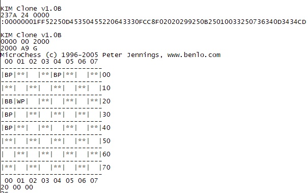
Now, I could use SecureCRT or Tera Term or some other fancy terminal to send the file as ASCII when I press the [L]oad command on the KIM-1.  Today, however, I will use the humble PuTTy terminal emulator.  And simply copy the hex to my clipboard, and paste it in PuTTy after pressing the [L] command.


KIM Clone v1.0B
237A 24 0000
:00000001FF52250D45350455220643330FCC8F02020299250B25010033250736340D3434CD

KIM Clone v1.0B
0000 00 2000
2000 A9 G
MicroChess (c) 1996-2005 Peter Jennings, www.benlo.com
 00 01 02 03 04 05 06 07
-------------------------
|BP|**|  |**|BP|**|  |**|00
-------------------------
|**|  |**|  |**|  |**|  |10
-------------------------
|BB|WP|  |**|  |**|  |**|20
-------------------------
|BP|  |**|  |**|  |**|  |30
-------------------------
|BP|**|  |**|  |**|  |**|40
-------------------------
|**|  |**|  |**|  |**|  |50
-------------------------
|  |**|  |**|  |**|  |**|60
-------------------------
|**|  |**|  |**|  |**|  |70
-------------------------
 00 01 02 03 04 05 06 07
20 00 00
?C
MicroChess (c) 1996-2005 Peter Jennings, www.benlo.com
 00 01 02 03 04 05 06 07
-------------------------
|WR|WN|WB|WK|WQ|WB|WN|WR|00
-------------------------
|WP|WP|WP|WP|WP|WP|WP|WP|10
-------------------------
|  |**|  |**|  |**|  |**|20
-------------------------
|**|  |**|  |**|  |**|  |30
-------------------------
|  |**|  |**|  |**|  |**|40
-------------------------
|**|  |**|  |**|  |**|  |50
-------------------------
|BP|BP|BP|BP|BP|BP|BP|BP|60
-------------------------
|BR|BN|BB|BK|BQ|BB|BN|BR|70
-------------------------
 00 01 02 03 04 05 06 07
CC CC CC

Personal Notes:

-The extended monitor on the KIM Clone has extra for string printing and more, so if I was doing a serious "KIM CLONE" port, I might look at rewriting a lot of the drawing functions.

-It is really clunky how the screen re-draws after every CHARACTER -- which means I have to sit through 4 board redraws just to enter a move.  I want to update that code, because I don't have pre-digital age patience.

-My cross compiler of choice is ca65, part of the cc65 C compiler for the 6502.  Maybe a ca65 port of the syntax is something I might try.

There are great usage notes for this version of the game here:

https://obsolescence.wixsite.com/obsolescence/kim-uno-microchess

Too late now, but I notice he went through the exact same process changing the UART routines for his version of MicroChess for the Arduino KIM-1 emulator.
KIM monitor as modified for the Corsham Tech KIM Clone board.
Notable changes:
* Removal of the code to save/load from cassette tape.
* Lunar Lander (First Book of KIM) added.
* Famer Brown (First Book of KIM) added.
* New X command from TTY to enter the Corsham Technologies xKIM extended monitor.
See also the Corsham github page.
Download the KIM Monitor repository copy here.
Note that you can use the standard KIM ROMs also, the KIM Clone is a KIM-1.