The Dutch KIM User Club published many articles by users on thet Elektor 6502 systems, like the Junior.
KIM KENNER 12
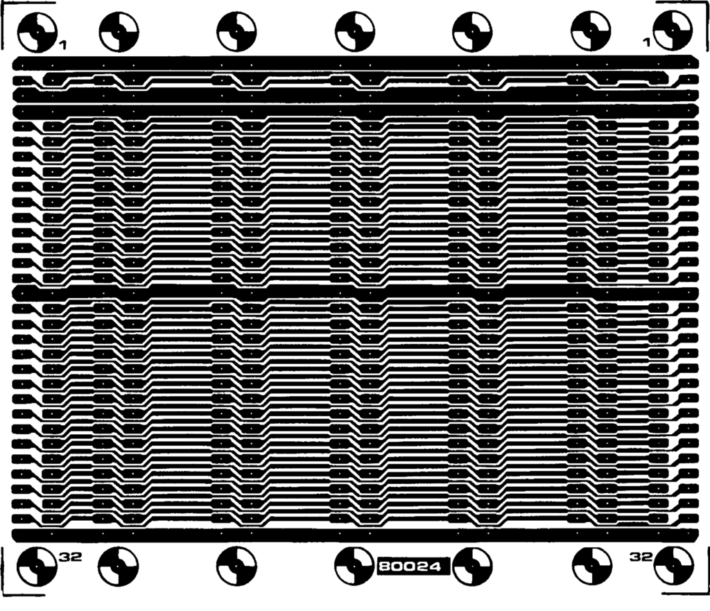
4 “De Junior” door Anton Muller
KIM KENNER 13 – 18 oktober 1980
4 Hex teller en flip flop voor de Junior, J. Hummeling
6 Ervaringen met de Junior computer, W.L. van Pelt
KIM KENNER 14 – 20 december 1980
4 JUNIOR, H.J.C. Otten
8 One armed Bandit voor de Junior, F.J. Butterfield
12 Ervaringen met de Junior, J. van Sprang en W.L. van Pelt
14 Junior leesroutine voor Kansas City cassette interface, Sebo Woldringh
16 Junior schrijfroutine voor Kansas City cassette interface, Sebo
De 6502 KENNER nr 15 maart 1980
13 Ervaringen met de JUNIOR J. van Sprang en W.L. van Pelt
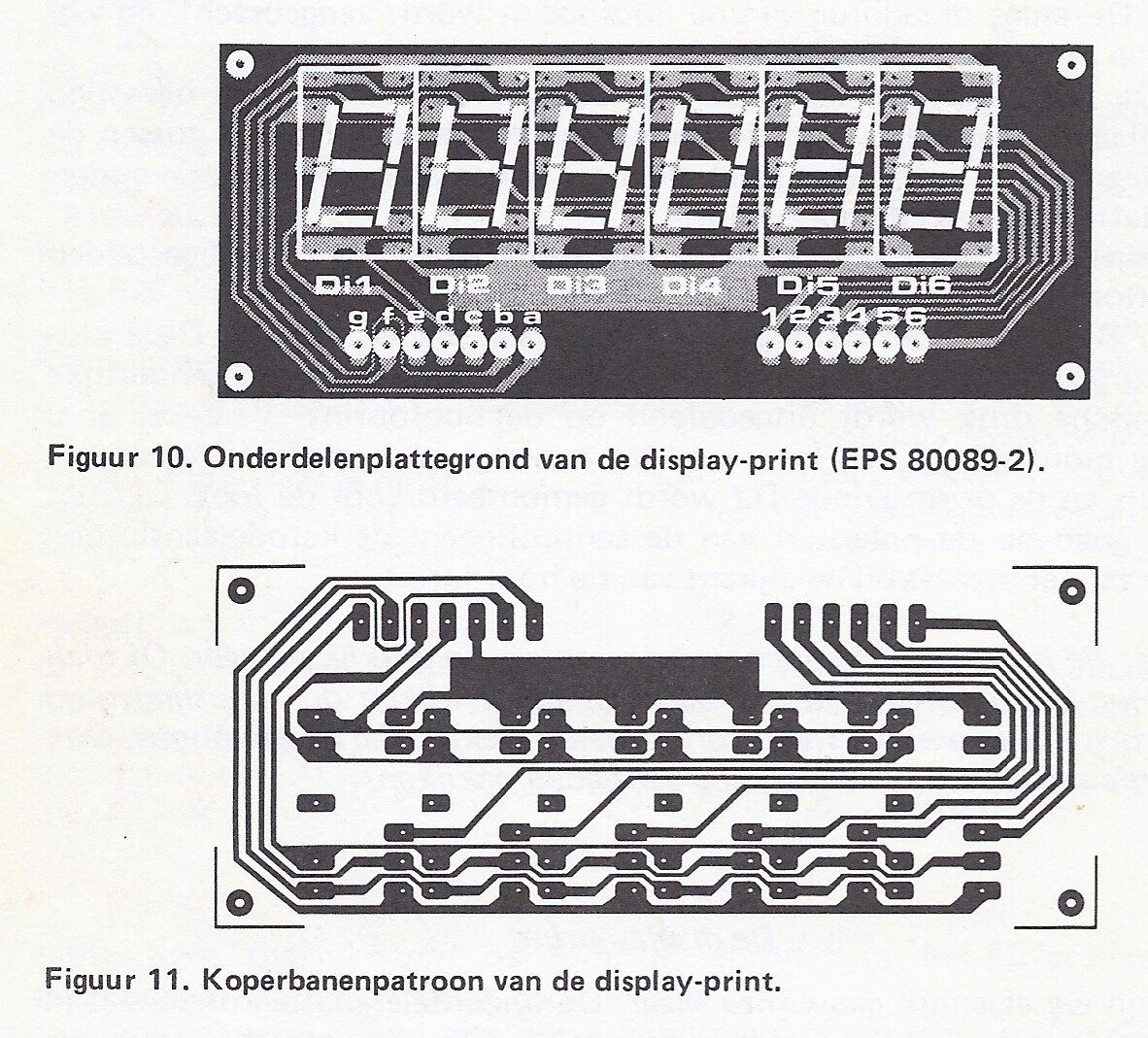
15 Letters en cijfers op JUNIOR display J. Hummeling
De 6502 KENNER nr 16 mei 1981
24 Ervaringen met de Junior, W. Van Pelt en J. van Sprang
26 Automatische register uitlezing voor de Junior
39 Browse voor de Junior
De 6502 KENNER 17 – augustus 1981
12 Ervaringen met de Junior, Willem van Pelt en John van Sprang
De 6502 KENNER 19 – december 1981
Schrijf- en lees routine voor de Junior, Dick Blok
15 Rapportcijfer, Rein Duyts
22 Display op oscilloscope, C. Totte
28 Aanpassingen aan de Macro Assembler van C.W. Moser, van Nieuwenhove Koen
34 Patches op Basic, Hans Otten
35 Lichtshow voor de Junior en de KIM, K. Kikke
38 4 kolom printer, A.S. Hankel
40 Printer routine voor H14, Paul de Beer en Hans Otten
43 Break voor Junior en KIM, Frans Mepschen
De 6502 KENNER 20 – februari 1982 LUSTRUM nummer
79 SYM Microsoft Basic aangepast voor de Junior, door Jaron Orenztajn
81 Aanvullingen voor de Elektuur EPROM programmer, door John van Sprang
85 Aanpassingen Junior print voor 2716, door J. Vollering
86 Bugs
87 Patches Micro Ade deel 11 voor de Junior, door A. Hankel
91 Voedingsschema voor +5V, +12V en -12V. door Frans Smeehuizen
92 Memory test aangepast voor de Junior, door Bert van Tiel
De 6502 KENNER 21- Mei 1982
36 Junior’s aan de PET, door Ruud Uphoff
De 6502 KENNER 22 – Augustus 1982
12 Patches op KIM-1 Basic t.b.v. de Junior, door Van Nieuwenhove Koen
De 6502 KENNER 23 – Oktober 1982
11 Patches op KIM-1 Basic t.b.v Junior (deel 2), door Van Nieuwenhove Koen
25 R.T.T.Y. met Junior, Telexberichten via korte golf op uw scherm, door A.S. Hankel
32 Easy Editing Supporter v. Junior, door R.C. Vissers
40 Simpele geheugenuitbreiding, door H. Burgers
43 Single Step Debug Programma, door M. A. v.d. Laan
46 Tiny Basic voor Junior + cassette routine, door Filip van Kenhove
De 6502 KENNER 24 – December 1982
14 Patches op KIM-1 Basic t.b.v Junior (deel 3), door Van Nieuwenhove Koen
4 Cassette bibliotheek, Junior cassette 2
De 6502 KENNER 25 – Februari 1983
6 Patches op KIM-1 Basic t.b.v Junior (deel 4, slot), en bugs in deel 1,2 en 3, door Van Nieuwenhove Koen
24 Junior en dubbel adressering VIA 6522, door Koen van Nieuwenhove
35 AIM-65 Basic voor de Junior, door E.J.M. Visschedijk
De 6502 KENNER 26 – mei 1983
4 ReNr en Append voor de SYM-Basic voor Junior
6 Maak van Junior een Senior: Disk drive Systeem van Proton op Junior, door P. Franssen
16 Printen op OKI Microline 80 Printer, een nieuwe printer routine voor Junior
De 6502 KENNER 27 – Augustus 1983
3 Proton’s JUNIOR DOS
3 Spiraal (KIM) nu voor Junior
19 Koppeling van Junior aan 8″ Floppy, met FD1771 controler 8″ single en 5″ double density, door Koen van Nieuwenhove
41 UART schakeling voor Junior, door A.A. Zwart
De
KIM KENNER 28 – Oktober 1983
6 Grafisch display voor Junior, door H. Christen
De 6502 KENNER 29 – December 1983
21 Read Junior’s SYM-Basic cassettes with Microsoft KB9 Basic
22 Toevoegen niruwe commando’s aan de SYM-1 Basic voor KIM-1 en Junior, Frans Smeehuyzen
25 Vraag en aanbod
26 Automatisch regels verwijderen, Frans Smeehuyzen
28 Boekennieuws
28 Clear screen voor JUNIOR’s SYM-1 Basic, Will Cuypers
29 Tekstverwerker, naar een idee van M.A. van der Laan
31 Hexadecimaal omzetter, Dick Blok
33 Universele geheugenkaart voor Junior
33 KB9-Basic op Acorn SYSTEM-1
39 Junior’s Hex monitor on Acorn-System, Alfons van de Meutter
De 6502 KENNER 30 – Februari 1984
8 Usurpator, schaakprogramma voor Junior, Fridus Jonkman
9 PACHA, patch on PM monitor, Fernando Lopez
11 Bouw eens een Miljonair: 2 miljoen bytes voor uw Junior, Jam H. Vernimmen
17 Program cassette 1: Junior/Apple formaat cassette routines deel 1, A Brouwer
34 LED’s op Junior, Hans Buurman
37 Uitbreidingen op SYM-1 Basic voor KIM en Junior: automatische regelnummering, Frans Smeehuyzen
39 Missing data in Junior Book 4
47 Load your Junior Sym-Basic Tapes into KB-9
De 6502 KENNER 32 – Juni 1984
21 KIM-1 en Junior KB-9 Basic Tokenized Microsoft Basic Keywords and addresses, Willem L. van Pelt
28 Aanpassen regelbreeddte via het toetsenbord, Frans SMeehuyzen
47 Extended AIM Basic Junior patch on Basic program compressor
4 Tips & Trics, Wout van Dinther en Gerard van Roekel
29 Junior Command Characters, Coen Kleipool
34 Basicode-2 voor de Junior met SYM-Basic, Fridus Jonkman
36 Hexdump voor de Senior Monitor voo Junior met PROTON’s monitor, Rob Banen
44 UART schakeling voor Junior, A.A. Zwart
44 Textfiles with Junior, Camiel de Ly
De 6502 KENNER 33 – Augustus 1984
3 Epson FX80 printer routine for Junior with OS65D
8 Junior disassembler voor hexdisplay, Fridus Jonkman
17 Low cost Elekterminal Expansion, R. Baarslag
24 Spiraal, grafisch op Junior met VDU kaart, Japp van Toledo
33 Tracer en single step, voortzetting uitbreidingen SYM Basic op Junior, Frans Smeehuyzen
De 6502 KENNER 34 – Oktober 1984
36 Save en load routines PROTON DOS SYM-1 Basic op Junior, Frans Smeehuyzen
33 HEX ascii dump, FORTH Gert Klein
39 Wallbreaker for Junior with OHIO-DOS, Willem Kuitens
42 Maanlander, Maarten van Hintum
44 Junior 8K of Junior 64K, Hans Mooi
De 6502 KENNER 35 – December 1984
5 Junior met VDU kaart Greedy spelprogramma deel 1, Phons Bloemen
48 Junior met D.O.S, Koen van Nieuwenhove Speed
De 6502 KENNER 36 – Februari 1985
5 Junior met VDU kaart Het grafisch display, J.J.A. en J.A.J. Janssen
21 FORTH op Junior deel 1, Gert van Opbroek
24 OHIO DOS V3.3 Aanpassen I/O routines, Wout van Dinther
24 How to change the Memory Map of your FORTH system on Junior
De 6502 KENNER 37 – April 1985
17 Junior met DOSV2.0A Bug in Disc patches on ASSM/Ted, Hans buurman
45 FORTH op Junior computer, Gert van Opbroek
De 6502 KENNER 38 – Juni 1985
11 Dubbele dobbelsteen Junior met PM Maarten Lamey
22 ID en KB-9 Microsoft Programs, Camiel de Ly
23 VIA ACIA print, M.A. van der Laan
32 Patches op PM Junior
40 Sorting subroutine Junior Fernando Lopez
De 6502 KENNER 39 – Augustus 1985
10 DOS65 JUNIOR, another DOS for the Junior, Coen Kleipool
12 Boekbespreking
13 Time of day, de 6526 nader bekeken, Ruud H. Uphoff
18 Vraag en aanbod
19 Junior met OS65D V3.3 Uitbreidingen, Gert Klein
33 Junior Tape I/O, A.W. den Hertog
35 Ervaringen met de PC-2 computer van Proton Electronics
35 HCC Computerdagen 16/17 nov 1985 reductiebon
36 Tokenized Microsoft Basic Keywords and addresses CBM40XX, CBM 80XX, Nico de Vries
46 Automatische dataregel teller
47 FORTH op Junior deel 3, Gert van Opbroek
De 6502 KENNER 40 -Oktober 1985
39 Junior in Apple, Frans Verberkt
42 C64JUN, Junior leest C64 tapes, R.A.F. Bens
De 6502 KENNER 41 – December 1985
6 Basic teksteditor OHIO DOS Junior, Maarten van Hitum
15 Screen editor V3.0 SCRED 3.0 Junior met VDU kaart voor Basic of Comal, B. de Bruine
De 6502 KENNER 42 – Februari 1986
9 Real-time clock voor de Junior, Clock IC MC146818, M.J. Stiphorst
15 Octopus 65, fout in publicatie FCU kaart Elektuur Special
24 Octopus 65 Let it be, Will Cuypers
26 GRAF V2.4 Routines grafische kaart, J.J. A. JAnssen
38 Basic programma Competitiestanden Handbal Elektuur Junior deel 1, Gerard Keet
De 6502 KENNER 43 – April 1986
16 65(C)02 Vervanging 6502 in Junior, Jan Vernimmen
17 Elektor’s octopus diskettes available
18 Basic competitie standen deel 2, Gerard Keet
23 Een wait ingang voor de Junior, Roger Langeveld
29 Octopus Diskette copier version 2.2, Wolfgang Tietsch
44 Bankswitching for the Junior, Fernando Lopez
De 6502 KENNER 44 – Juni 1986
1 Inhoudsopgave
2 Alternatieve Break routine tbv CPU kaart, Frans Smeehuyzem
4 Elektor’s OCTOPUS/EC65 computer: A data buffer as afterthought, R.T. Overakker
6 Problem with EC65 poweron reset, Siegfried Losensky
7 Elektor’s Octopus/EC65 Modified diskette copier version 2.2 part 2
18 Junior interface card en gewijzigde VDU card, Pieter de Visser
21 Junior POSVAL Chessmonitor for Elektor with hexdisplay, Frans Raaijmakers
21 EC65 Patch realtime clock
29 Printer initialisation for EC65, Leif Rasmussen
29 EC65 SAMSON tips, Leif Rasmussen
31 Basic competitiestanden part 3, printroutine voor teletype 110 baud
38 Junior with Proton’s Senior monitor modified format lister, Rob Banen
45 6845 geprogrammeerd
48 Delete character routines tbv de Elektor VDU card
De 6502 KENNER 45 – Augustus 1986
3 Elektors EC65 Starcatcher Basic game
42 Junior with VDU OHIO DOS NUMBERS routines to handle input of numbers from the keyboard
12 Realtime clock 146818 IC routines, Frenando Lopez
21 Elektor VDU card modification, J.C. Rix
22 New Centronic routine for Junior/Octopus 65, Coen Boltjes
25 Junior POSVAL Chessmonitor for Elektor with hexdisplay, Frans Raaijmakers
43 Basic competitie standen deel 4, Gerard Keet
46 Use of cursor control keys ED, Rene Hettfleisch
46 Octopus/EC65 disks
De 6502 KENNER nr 46 – october 1986
5 Block graphics on EC65: screendump, Leif Rasmussen
6 An interrupt decoder for the 6809, Andrew Gregory
8 8K RAM voor de Atom, Karel Odon
8 Patch on Dr Tietsch’s copier program, Marc Lacheart
9 A macro loader and Saver for ED DOS65, Bram de Bruine
11 Bitpatroon voorde C64, Gerard van Roekel
11 TIP: 0 in data regels plaatsen, Gerard van Roekel
12 Basicprogrammas’ combineren 2 en 3 letterwoorden, Gert Kwetters, Bart van Pelt
13 Junior bekent kleur, Phons Bloemen
17 Look at real contents Atari, Henk Speksnijder
17 Modification VDU card Octopus65, Albert v.d. Beukel18 Junior POSVAL schaakmonitor part3 end, Frans Raaijmakers
18 Junior Changing the 6502 by a 65C02. Jan Vernimmen
19 Troubles with Micro Ade and Elektor’s Octopus, Marc Lacheart
19 Solution of Micro Ade problem of contineous erros, Ronald Hermans
20 Junior malfunction Display, Ronald Hermens
21 Directory Disk1 ‘System Loys diskette’, Fernando Lopez
22 Bell routine for Octopus/EC65 with Basicode interface card, Coen Boltjes
22 Junior POSVAL wijizigingen in gepubliceerde listing, Frans Raaijmakers
23 Error messages Junior, adapted for Junior, Ronald Hermens
25 PL3/4 straps poblem CPU card, Frans Smeehuijzen
30 Patch in the Octopus/EC65 standard monitor, Marc Lacheart
30 Patches on Disk 5A (Original OSI V3.3) Marc Lacheart
31 Problemen met de Octopus65 met RS232 printer, J.A. van Eken
De 6502 KENNER nr 47 – December 1987
4 Hardware adjustment Junior/Octopus with VDU card for use as a videotext terminel Prestel standard, Coen Boltjes
6 How to adjust the character generator for Videotex, Coen Boltjes
8 Junior Break key with serial keyboard, Gerard van Woerkom
12 Directory Disk 5a Ohio DOS
12 Junior dubbel adressering, Frans Bens
18 Tips and tricks for the EC65K/Junior, Coen Boltjes
19 MON65 op Junior, Erik v.d. Broek
20 The Junior Computer revisited, Fernando Lopes
28 Bell for EC65, Rasmussen and Lindstroem
32 Extension of OS-65D V3.3 with DEL command
38 Screen flickering, Andrew Gregory
38 Slave: bootstrap loader Junior, Ronald Hermens
39 TELEX programma MCB 1984, Marcel Breukink
44 Columns print for printing in two columns, Octopus, Leif Rasmussen
45 Hardcopy routine for Octopus, Coen Boltjes
De 6502 KENNER nr 48 – February 1987
5 Videotex program for the Junior Octopus, Coen Boltjes
26 Ascii dump with OS65D extended monitor, Gerrit van Woerkom
28 Working with Micro Ade and bankswitching on the Junior Computer, Fernando Lopes
De 6502 KENNER nr 49 – April 1987
7 EC65/Octopus Screendump for Kolorator, Leif rasmussen
11 Plotpoints Atari 520ST, Jan Vernimmen
16 Expansion for Ohio DOS Extensions, Coen Boltjes
25 EC65/Octopus How to get more memory space, Peter Linstrom
29 DOS65 ACIA 65C51 and modems. Bram de Bruine
31 Centronics input for DOS65 or Junior computer, Ernst Elderenbosch
32 How to modify the Elektor 64K memory card for use with DOS65, Andrew Gregory
33 Hoe wordt de video controller 6845 geprogrammeerd
39 Forth on the Junior, Frans Bakx
43 Maanlander Junior, Fridus Jonkman
46 Printer routine for Junior, Alfons v.d. Meutter
De 6502 KENNER – nr 50, Juni 1987
4 Fast alternative for the slow Junior cassette interface and software, Hans Christen
8 Solved problems Octopus vdu card monitor EPROM
19 Relocator for DOS Junior and Octopus 65, Coen Boltjes
21 RAM Test program for the Octopus 65, Marc Lacheart
36 Paperware service EPROM programmer for Junior, Andrew Gregory
De 6502 KENNER nr 51 – Augustus 1987
9 EC65/Octopus cassette motor control and Bell hardware, Marc Lacheart
17 EC65/Octopus Wordprocessor V3.0 available, Leif Rasmussen
17 EC65/OctopusPatch on Dr. Tietsch Copier program, P. Lindstrom, Leif Rasmussen
17 Printer problems with the Octopus, Maarten den Hertog
21 Loys extra, how to bind the systemdisk utilities, Leif Rasmussen
28 Junior tape routines on DOS65, Ernst Elderenbosch
26 Octofate: Fate for the Octopus, Coen Boltjes
26 Octopus inputverwerking, A.P. Oerlemans
De 6502 KENNER nr 52 – October 1987
25 EC65 EPROM disk loader
27 EC65 EPROM disk directory
32 EC65 NUMINT basic
34 EC65 Language study help
37 Junior MAZE
De 6502 KENNER 53 – december 1987
30 EC65 Modified version of Elektor’s listing stopper
De 6502 KENNER 57 – Augustus 1988
34 DOS Errors in words EC65
De uPKenner 61 – April 1989
28 EC65K EPROMs programmeren
COMPUSER Volume 1 Nr 2 March 1988
16 Screen noise on Junior with VDU: synchronize CPU and VDU
17 A description of the DOS65 Disc format
24 Tape backup and restore utility OCTOPUS/EC65, Marc Lachaert
35 OHIO DOS V3.X special for Junior, Dirk Picke
COMPUSER Volume 1 Nr 5 March 1988
1 Fractals in assembler EC65 Leif Rasmussen
COMPUSER Volume 2 Nr 1 January 1989
14 Transfer OCTOPUS into a development system, Peter F. de Pauw
34 Read time and date EC65, Peter lindstrom
38 Junior DOS65 Erik vd Broek
See also:
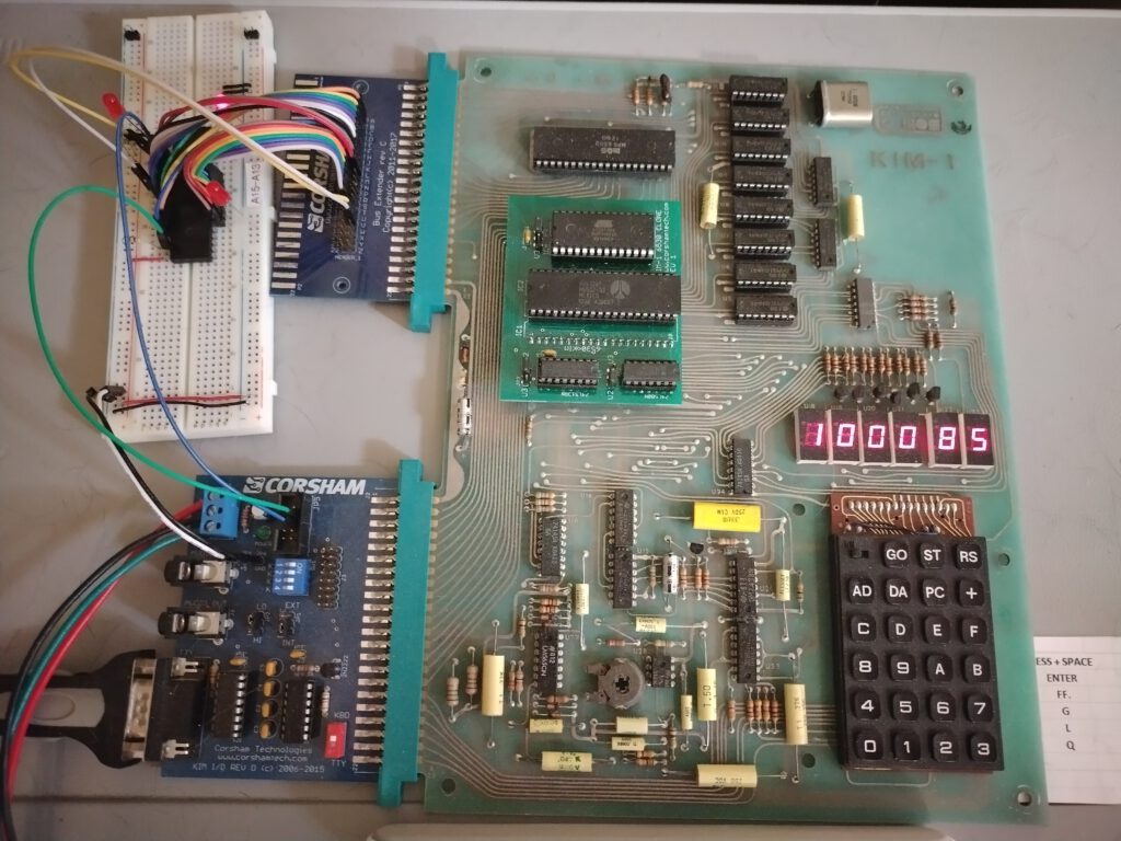
KIM-1 Simulator documentation
KIM-1 Simulator
Hans Otten, Eduardo Casino, 2019- 2026, Version 2.0.0 beta
Contents
Introduction
Installatio...
DIY KIM-1 Keypad
A spare KIM-1 keypad is even rarer than a KIM-1 itself. With this guide you can build a reasonable replica of the ke...
Proton PIM-1
Gerben Voort acquired a microprocessor development system PIM-1 developed by Proton, of PC-1 fame.
Here his photos of...
PROTON Electronics: PC-1, CB80, PIM-1
PROTON Electronics, a small company from Naarden the Netherlands, led by James Post, and A.J. Kool as technical manager,...