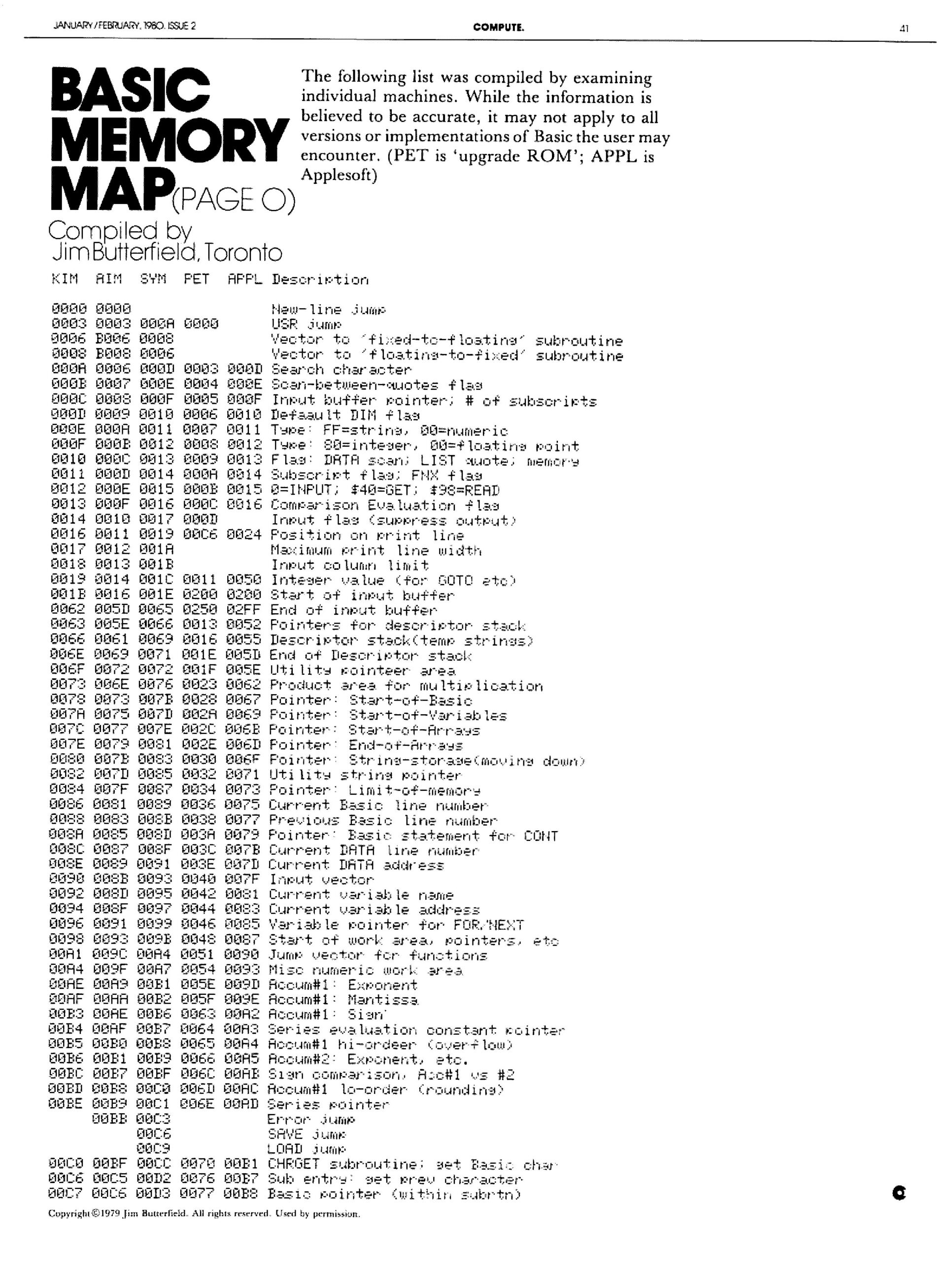
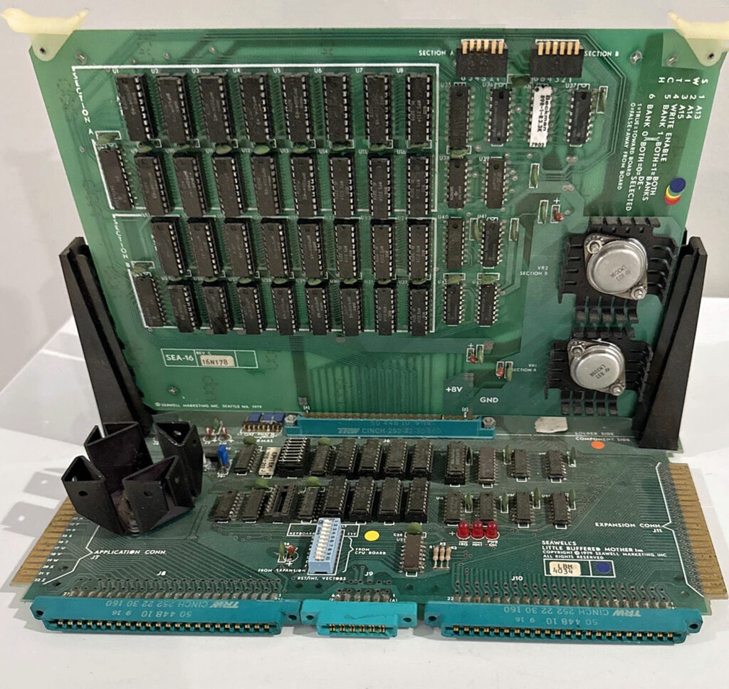
A passive card cage and 4 -slot bus for KIM-1, SYM-1, AIM 65 and PET Commodore.
Note that the KIM/MTU bus is still in use in the replica boards series designed by Eduardo Casino, see his repository here for buffered and an unbuffered version.


All MTU expansions, be it card cages with motherboards, memory, video, floppy disk cards use the MTU/KIM-1 bus.


PRINCIPLES OF OPERATION
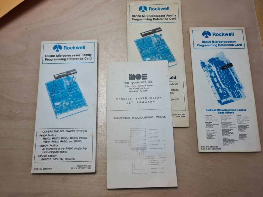
Actually there is not much theory behind the operation of 5 edge connectors, 44 parallel wires and a terminal strip. What can be discussed however is the philosophy behind the K-1005 series of card files and its associated KIM/MTU bus. The Commodore KIM-1 single-board microcomputer was first released in 1976 and is the grandparent of the Synertek SYM-1 (formerly the VIM-1) and Rockwell AIM-65 micro-computers. Even the Commodore PET shows some KIM-1 influence. These processors cover the vast majority of 6502 based systems in use today and are the ones supported most vigorously by MTU.
WHY THE KIM BUS?
The original KIM-1 was a well thought-out product that hit on just the right tradeoff between system resources and selling price. Some amazing things have been done in its 1K memory such as the first generally available microcomputer chess program, the first 4 voice all software music synthesis program, Tiny BASIC, and others. However at some point every system needs to be expanded and the KIM and its relatives are no exception.
Commodore’s answer for expansion was the KIM-4 expansion bus and KIM-3 memory board. Independent manufacturers introduced similar expansion bus boards while others offered expansion systems based on the Altair (S-100) bus. The S-100 bus adapters were more successful because there was a multitude of expansion boards from which to choose. One pitfall in the S-100 technique is that not all S-100 boards would work properly with 6502 timing signals. The main common fault with the mechanical implementation of these products is their open-air construction which offers little protection for the boards and eliminates portability.
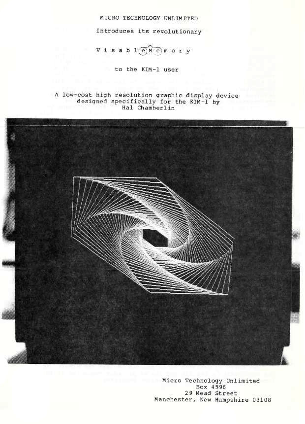
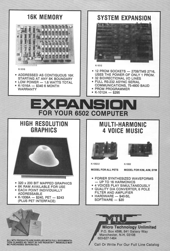
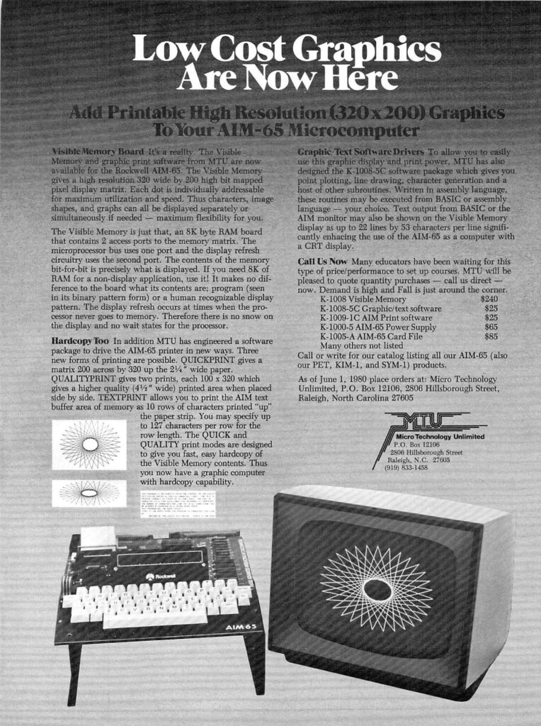
MTU’s first KIM expansion product was the K-1008 Visible Memory. The idea behind the VM was to have a board at the price of a plain 8K memory which would also show a high resolution video image. The goal was to capture both the KIM add-on memory and video display market with a single product. In deciding how it should connect to the KIM we had several factors to consider. First, it seemed like a poor idea to produce a board to plug into a bus (KIM-4) that few potential customers had. On the other hand an S-100 environment would have prohibited our use of 6502 timing properties to produce a totally transparent memory and snow-free display. In the final analysis it seemed desirable to produce a board that re-quired no motherboard or bus at all to connect and thus be available at a much lower “installed” price. The logical conclusion was simply direct parallel connection to the KIM-1 Expansion connector!
The KIM BUS, which is the signals on the KIM’s expansion edge connector, for the most part uses the actual signals from the 6502 microcomputer itself. Further-more the SYM-1 and AIM-65 Expansion connector busses are for practical purposes identical to the KIM-1 bus. The combined number of these processors sold makes the KIM bus one of the most widely used and to date has suffered less from compatibility problems than any other multi-vendor personal computer bus structure.
We have since designed and manufactured 4 additional expansion boards that may be used alone in the same manner. In order to support those customers who wish to use several of our expansion boards, we designed the K-1005 motherboard/card file which is simply a convenient method of connecting several boards to the processor’s expansion connector along with the necessary mechanical support provisions.
PLAIN OR BUFFERED?
Probably the most frequently asked question regarding the K-1005 is “Why is the bus not buffered?”. The basic answer is that buffering is not needed for only 4 expansion boards. The next question then is “Why not buffer it anyway to reduce microprocessor loading, provide noise immunity, and improve signal rise times?”. The answer to that is somewhat more technical but in a nutshell buffering has some of its own problems and it is not necessarily true that it improves system operating margins when the unbuffered equivalent does not violate any loading rules.
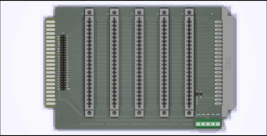
The KIM bus address and data lines are simply the corresponding microprocessor busses brought out to edge fingers. The various control signals (PHASE 2 and READ/WRITE) are indeed buffered by TTL gates on the processor board. The unbuffered address and data lines are rated by the microprocessor manufacturer to drive 1.7MA of DC loading and 170pF of capacitance. This figures out to 5 low power Schottky TTL (74LS series) inputs (MOS inputs such as to memory IC’s have no DC load) and about 35 circuit connections at 5pF per connection. The processor board itself uses one low power Schottky load and about a dozen connections (more connections on SYM and AIM processors). This leaves 4 low power Schottky inputs and over a dozen connections for the external bus which is adequate for implementing a 4 slot expansion bus. This is the main reason the K-1005 has 5 slots including processor.
Probably the most misunderstood aspect of buffering is noise generation and immunity. In theory low impedance TTL or TRI-STATE bus drivers should be able to “short out” noise spikes much better than high impedance MOS outputs can. This may be true, but in practice TTL or high power TRI-STATE bus buffers generate so much noise when they switch that almost nothing can absorb it. The problem is most acute in large systems (such as minicomputers and S-100 computers) where as many as 24 buffers with 100MA surge capability and nanosecond rise times can switch simultaneously thus placing a 2.5 amp reaction current surge through the GROUND leads of the bus. It is not unusual to see over a half volt differential in GROUND voltages between driving and receiving boards in such a system. In practice such spikes interfere with the bus CONTROL signals which results in unpredictable occurrances such as spurious writing into memory or falsely triggering an I/O device. Seldom are address and data bus signals themselves read wrong even though they cause the noise because they are ignored while changing (under the direction of control signals). indicate that all changing must have ended and the data be stable at it’s “0” or “1” state. It is instructive to note that minicomputer busses (such as the DEC UNIBUS and the NOVA bus) specify the use of filter and delay circuits on control signal lines received by interface boards. In addition, these systems typically have multilayer backplanes with ground planes to shield and shunt noise.
With unbuffered MOS and low power (8 MA) 74LS TTL bus drivers, such noise is almost completely absent. The author has had considerable experience in designing and troubleshooting bus systems and the unbuffered KIM bus is among the quietest encountered. With respect to rise time, 8MA is sufficient to swing 170PF (which is actually a rather heavy bus load) from logic zero to one or vice-versa within 65NS which is quite adequate for 1MHz 6502 operation. Note that this time has already been factored into the 6502 timing specifications. Remember also that bus buffers do have their own propagation delay times.
KIM BUS -VS- KIM/MTU BUS
As the reader may have guessed, the bus implemented on the K—1005 motherboard is not strictly a KIM—I bus. If it were, all 44 lines would be run strictly parallel up and down the board. The MTU modification amounts to assigning the top slot to the CPU (except for the PET version where all slots are equivalent) and not connecting some of the pins to the expansion bus below. This then frees up several lines on the expansion bus for other functions that do not relate to the CPU or computer bus operation,
Two of the pins are used to provide unregulated +8 and +16 volt power to the expansion boards, which the CPU does not use, Two more pins are used for the DECODE ENABLE and VECTOR FETCH signals that KIM-I systems require (unnecessary for AIM—65 and SYM—1). An additional three pins are used (in PET systems only) to carry separated Vertical, Horizontal and Video signals to a separate sync video monitor. Finally there is one spare set aside for future use. The following page lists the signals of each processor and those of the KIM/MTU bus used on the K-1005.
In providing these expansion bus signals, some signals from the CPU are not available on the bus, The most significant of these are READY and PHASE 1, PHASE 1 is equivalent to PHASE 2 the inverse of PHASE 2 which is available on the bus, Modern memories are fast enough so that wait states are not needed, thus the •READY signal. is of no use, Besides, the 6502 will not wait during a write cycle anyway.