Letter from Bill Mensch on the creation of the 6530
Bill Mensch wrote: I would be happy to contribute some commentary concerning the creation of the 6530 at MOS.
What are you interested in other than it was the second chip for the combination of the 6502 for use in control systems.
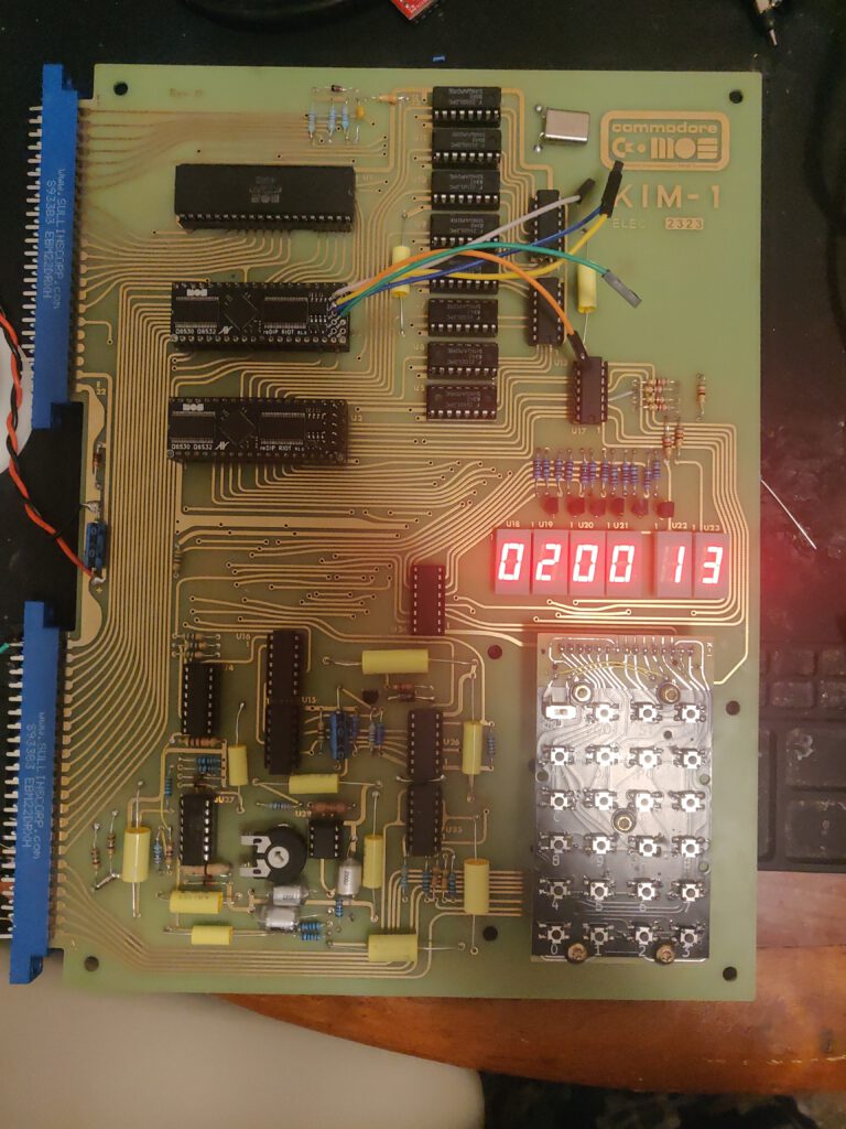
The KIM-1 was a reference design/use case for bothe the 6502 and the 6530, actually two of them.
One 6530 was for the “Teletype Input Monitor (TIM)” and the other one was for the “Keypad Input Monitor (KIM)”.
It was first demonstrated along with the 6501/6502 at the WESCON ’75.
The 6502 and 6530 were ment to compete with the $29 Intel 4040 two chip controller combo.
The actual design was important for the introduction of the 6502.
I and a team of three mask designers Harry Bawcom, Mike Jaynes and Sid Holdt created the 6530.
The timer design was patented and used on the 6530, 6531 and 6532 chips.
Chuck Peddle and Wil Mathys contributed the system level applications concepts and requested the features.
We were a small team. I was the semiconductor design and architect engineer.
The 6530 followed many of the design concepts of the 6820/6520/6821/6520 concepts for IO and interrupt features.
The 6522 followed the 6520/6530/6532 designs at MOS.
Ray Hirt was the project lead on the 6532.
The 6532 RIOT design was basically to remove the ROM and add another 64 bytes of RAM for a total of 128 bytes.
I was the microprocessor design manager at this time replacing Rod Orgill who had left MOS to work at NCR in Colorado Springs, CO.
Rod didn’t work on any of the IO chips, just the 6501/6502.
Ray, Rod, sometimes Wil and I shared many a pitcher of beer at many lunches after the 6502 and 6530/32 were completed before Rod left for Colorado.
These are fond memories of my time at MOS.
Since the 6532 is in fact a subset of the 6530 (no ROM, more RAM), it seems not too difficult to make a 6532 replacement this way.
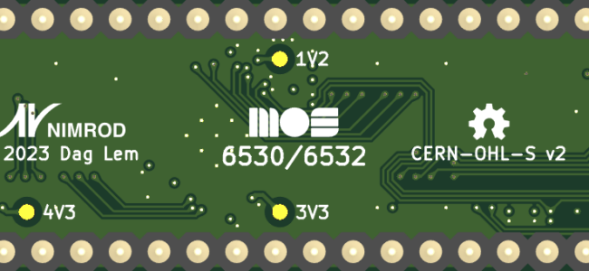
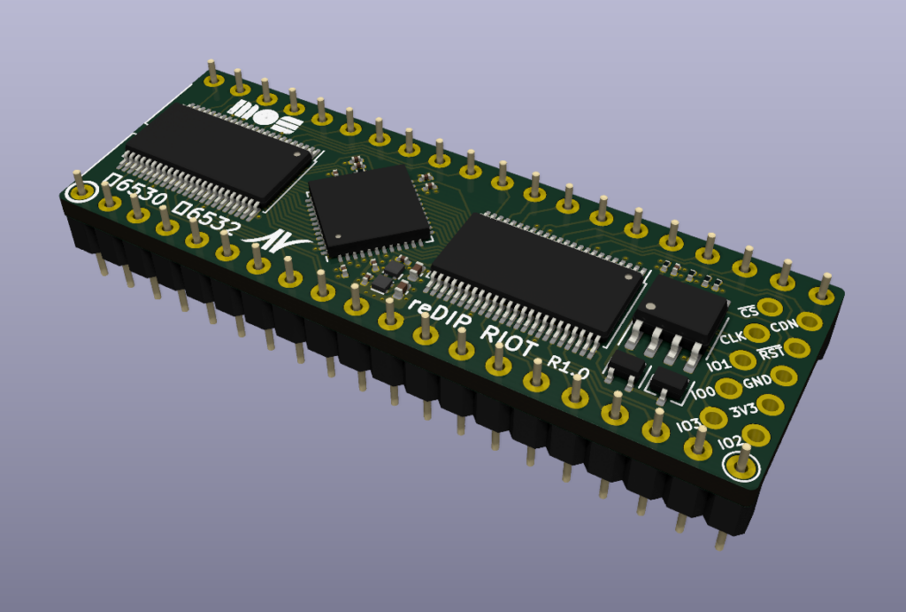
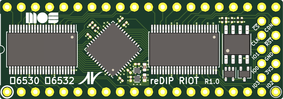
The reDIP RIOT is an open source FPGA board which combines the following in a DIP-40 size package:
Lattice iCE40UP5K FPGA
1Mbit FLASH
5V tolerant I/O
The reDIP RIOT provides an open source hardware platform for 6530 RRIOT / MOS 6532 RIOT replacements.
Since the 6532 is in fact a subset of the 6530 (no ROM, more RAM), it seems not too difficult to make a 6532 replacement this way.
The reDIP RIOT is an open source FPGA board which combines the following in a DIP-40 size package:
Lattice iCE40UP5K FPGA
1Mbit FLASH
5V tolerant I/O
The reDIP RIOT provides an open source hardware platform for 6530 RRIOT / MOS 6532 RIOT replacements.
4 february 2025 2025 I have built the PAl-2 kit, now designing and building a I/O card.
This information is based upon the available documentation: User manual, Schematic, BOM.
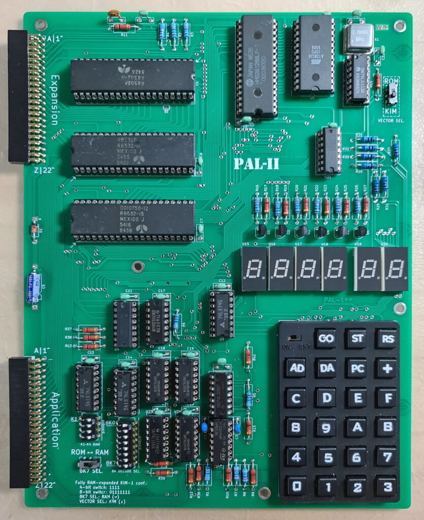
The PAL-2 is for sale by Liu Ganning at Tindie
Just followed the interactive BOM, passive components first, ICs last.
Nothing special to note, compare yours with the photo on the PAL-2 Tindie site.
Orientation of IC sockets and IC’s, check twice!
Check your soldering joints, not too much sodler, but covered with the right color solder.
And the three slider switches,: the SST keyboard one has a higher slider that the other two!
Please be careful with the Dupont power cables, double check the polarity! If in error: magic smoke!
I do not like the Dupont wires for power, serial, TTY switch. Too easy to make a mistake in the power connection.
I am now designing and building a simple I/O card for the Application connector, experimenters print, point to point wires, male pin connector to PAL-2, on board female connector for USB to Serial, power switch, TTY/Keypad switch.
That may grow later to SD or 1541 or Corsham SD card interfaces.
Video of PAl-2 #4, by Nils, running!
What is a PAL-2?
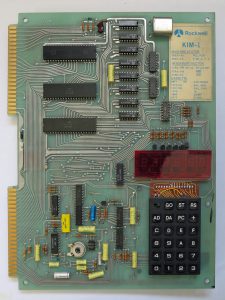
The PAL-2 is a kit for an SBC in the now large family of KIM-1 clones. Ranging from the Micro-KIM to the PCB exact replica by Eduardo Casino, all share the KIM-1 ROMs, LED display and TTY interface and the 6532 RIOT instead of the 6530 RRIOT.
What makes the PAL-2 unique:
It is a real and complete KIM-1 clone.
Available as a DIY kit with high quality components.
The layout is close to the KIM-1.
The good looking keypad is very close to the KIM-1
Application and Expansion connector with all relevant KIM-1 signals.
Lots of RAM in many configurable options.
Both RRIOTS 6532 on board.
TTY interface on TTL level, USB to TTL adapter included in the kit, quality serial!
Power can come from the USB to TTL adapter or from external 5V supply (same as for the KIM-1)
The PAL-2 differs from a KIM-1
No Audio cassette interface for file I/O circuit, but see below for a solution
Application and Expansion connector as 22×2 pinheader instead of PCB edge connectors
The signals on the Application connector are not all identical: no audio, TTY instead of 20 mA loop, decoding lines added
Not the same size PCB
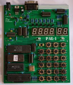
The PAL-2 differs from the PAL-1:
The many quality improvements and enhancements make the base PAL-2 kit more expensive then a base PAL-1 kit.
If you expand the PAL-1 to the level of a PAL-2 you need to spend money on a motherboard, a RAM 32K, a second RRIOT kit, an RS232 cable and gender changer and a 9V power supply.
Improved keypad, with labels and look of the KIM-1
No need for a Motherboard
No external RAM module required
No external RRIOT required
E000-FFFF can be used freely from ROM expansion
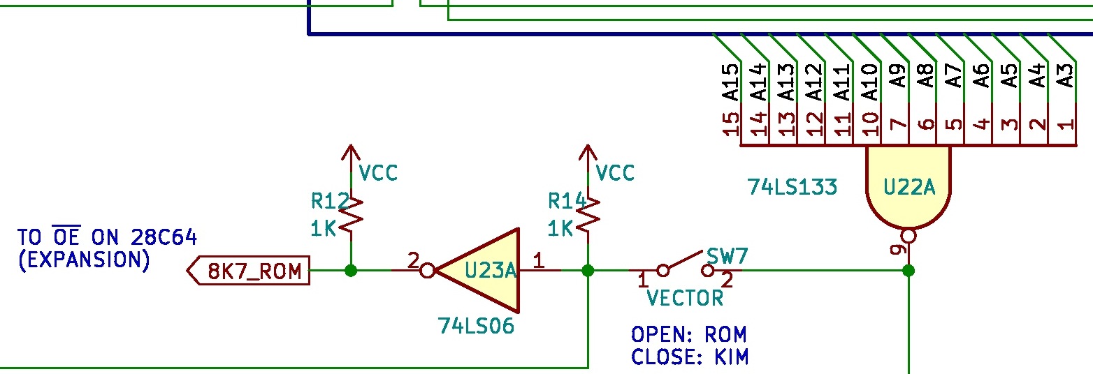
The vectors (Reset, NMI, IRQ) can be placed in external ROM.
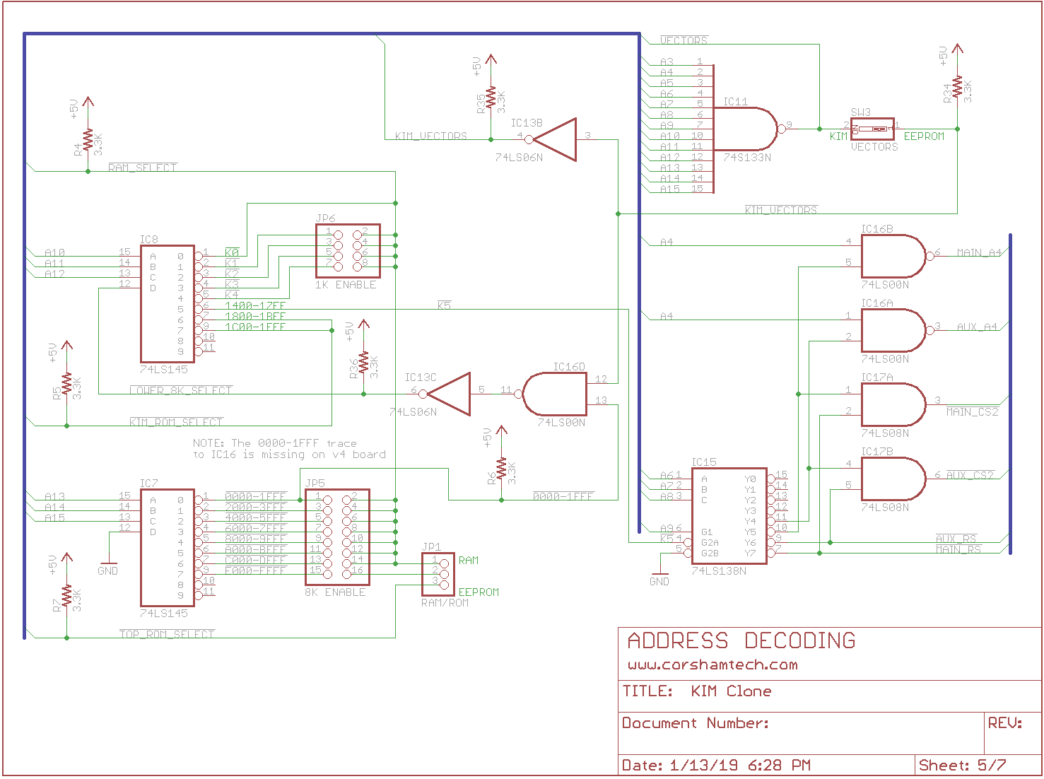
RAM decoding
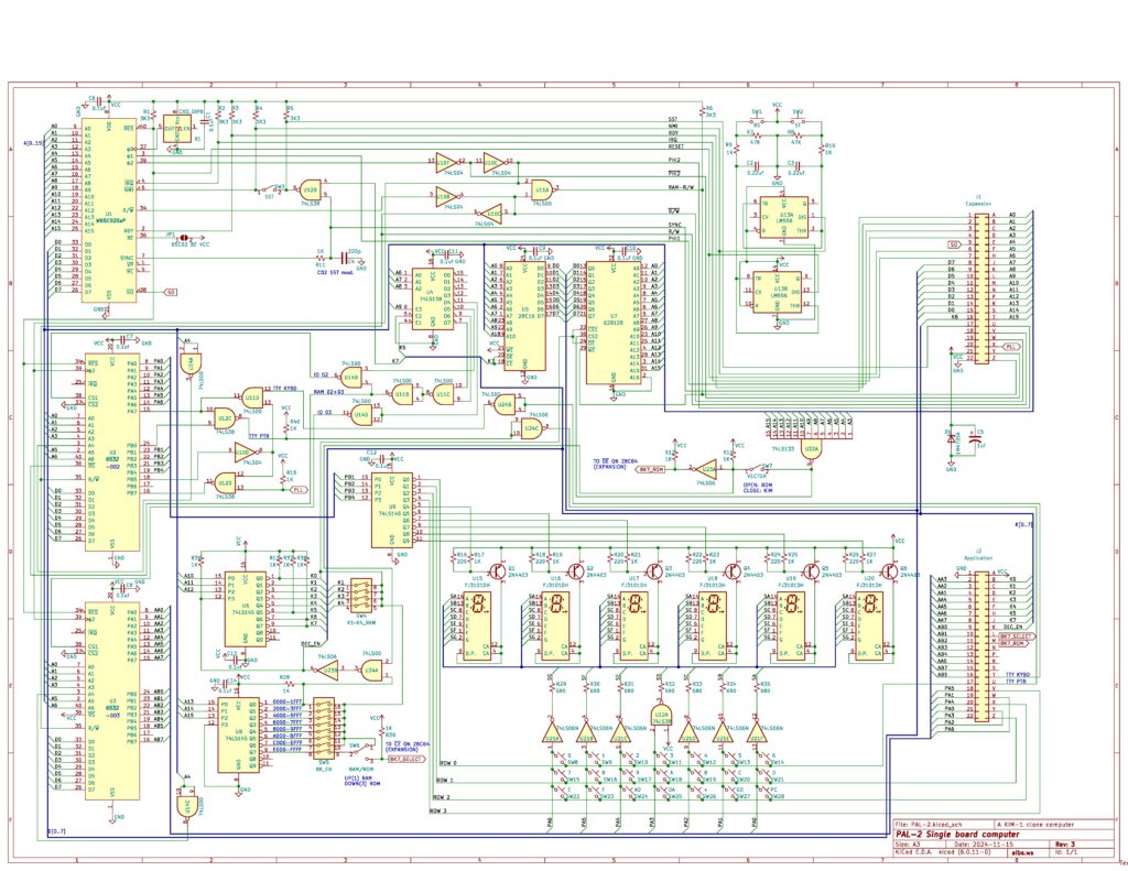
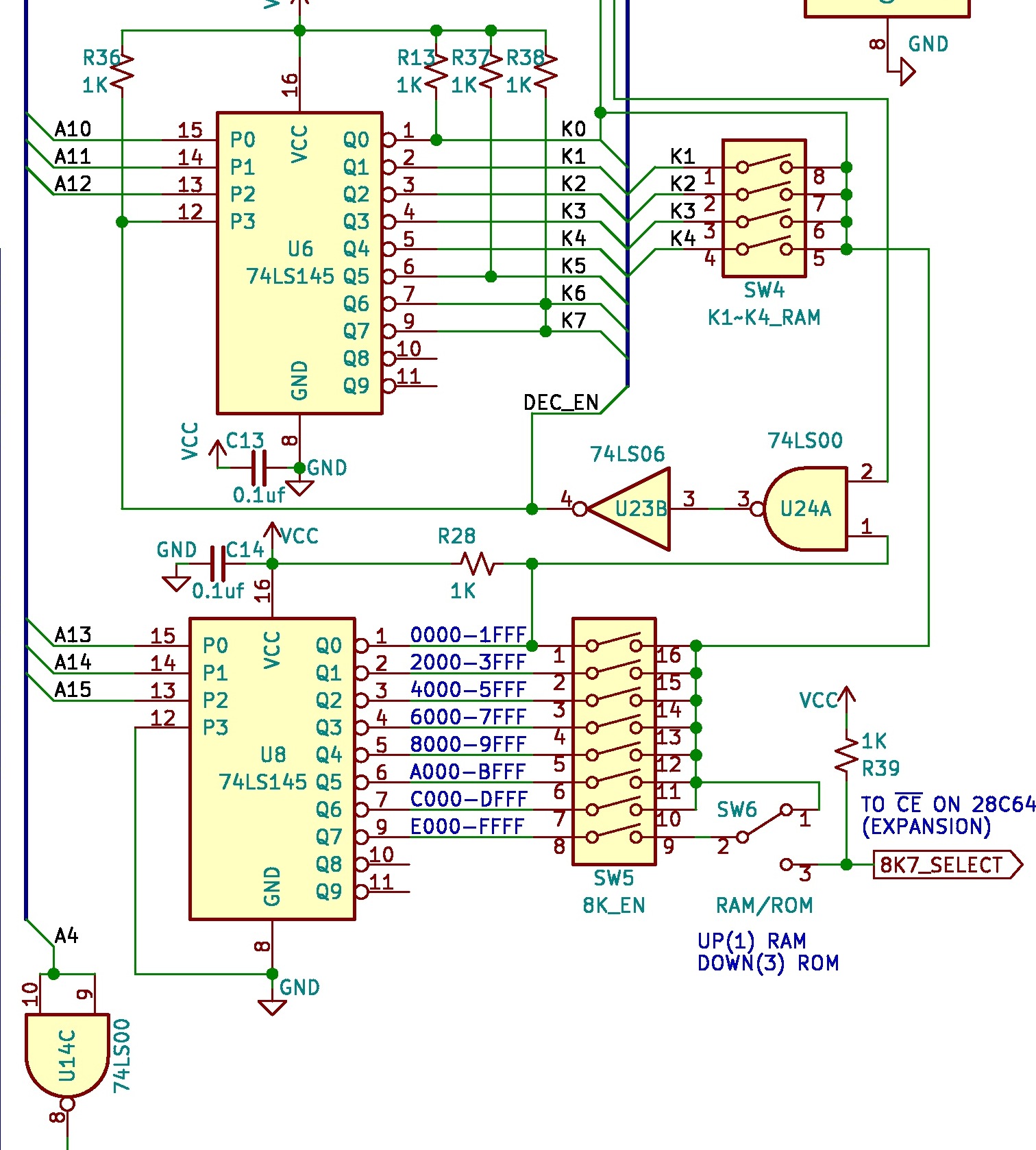
The PAL-2 has a very flexible RAM memory layout, as shown in the next parts of the schematics:
Internal ROM and external ROM
The PAL-2 has a 2K ROM with the KIM-1 monitor. Since there is no audio in and out circuitry, the ROM from 1800-1BFF could be used for other programs, like the KIM Clone by Corsham Technology (Which also did not have the audio circuitry). The 28C16 is easy to program.
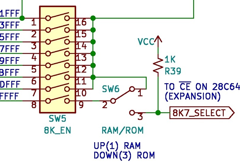
One of the first expansions that is to be expected is an external 8K ROM. The decoding for this ROM, e.g. an 28C64 is already present on the connectors and in the decoding circuit.
The decoding signals are 8K7_SELECT (CE on 28C64) and 8K7_ROM (OE on 28C64). Just the 28C64 IC has to be connected to address and data lines.
DIP Switches
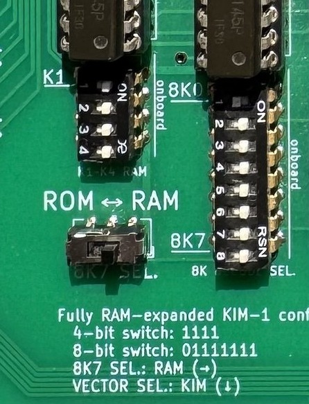
The PAL-2 has a full 64K address decoder onboard, while the KIM-1 has only a 5K onboard address decoder for expansion. These two DIP switches on the PAL-2 are designed both to expand the KIM-1’s RAM and to maintain compatibility with its basic configuration.
On the PAL-2, the 4-bit DIP switch enables the onboard K1 to K4 RAM spaces, with each bit controlling 1K of memory. The K1 to K4 naming follows the definitions in the KIM-1 user manual, covering the address range from $0400 to $13FF. If all four DIP switches are set to ON, the entire 5K RAM space becomes available to the system.
The 8-bit DIP switch controls the “big segment decoder,” with each bit corresponding to an 8K memory block. These blocks range from 8K0 to 8K7, with 8K0 ($0000 to $1FFF) being the KIM-1’s default occupied address space. Since the PAL-2 is a KIM-1 replica, if you want to use it as a KIM-1 system, 8K0 must be set to OFF to allow the onboard KIM-1 logic to function. However, if you’re building a completely new system on the PAL-2, you can set 8K0 to ON to bypass the KIM-1’s onboard logic for the lowest 8K of memory.
The 8K1 block starts at $2000, controlling an 8K space beyond this address, and so on. If a bit is set to ON, the KIM-1 system will be able to access the corresponding address space, which will function as RAM. If a bit is set to OFF, the KIM-1 system will still work, but with reduced available address space. When performing expansion or add-on modifications on the PAL-2, you may need to disable certain address spaces to prevent the onboard logic from accessing the RAM chip.
The 8K7 block, representing the highest 8K memory segment, offers additional flexibility on the PAL-2. If 8K7 is set to ON, you can choose how to use this space—either as RAM or ROM—by adjusting the 8K7 SEL switch. For example, if you write a program (such as a tiny OS for the KIM-1) and burn it onto a ROM chip—similar to the well-known Jim’s ROM (but smaller)—you can connect the ROM to the PAL-2 (with some additional hardware, which is still under development). To boot from your ROM chip, use the VECTOR SEL switch to select ROM, allowing the system to retrieve the top three vectors from the ROM chip instead of the onboard KIM-1 ROM.
Application and Expansion connectors
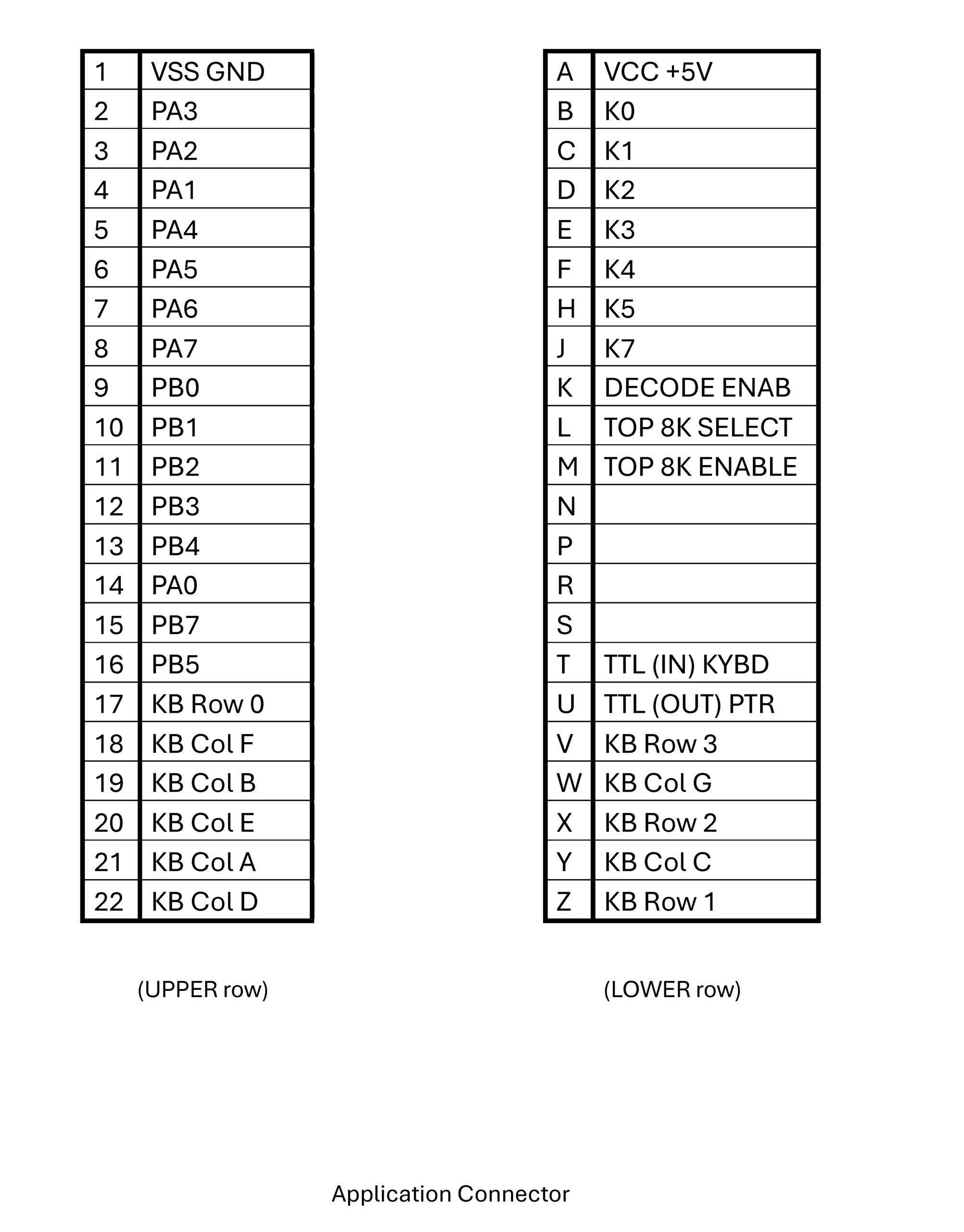
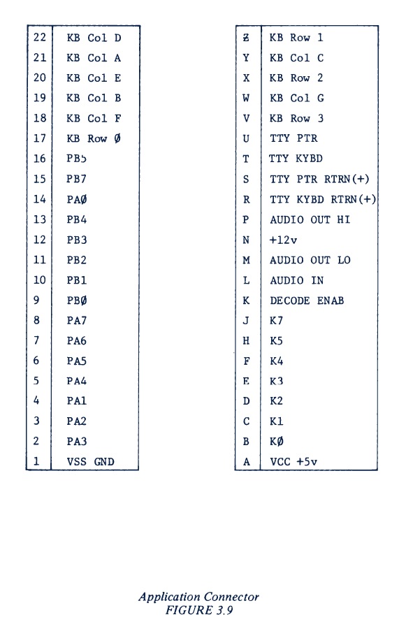
KIM-1 Application connector
Differences on the Application connector with the KIM-1:
AUDIO IN -> 8k7_SELECT
AUDIO OUT LO -> 8K7-ROM
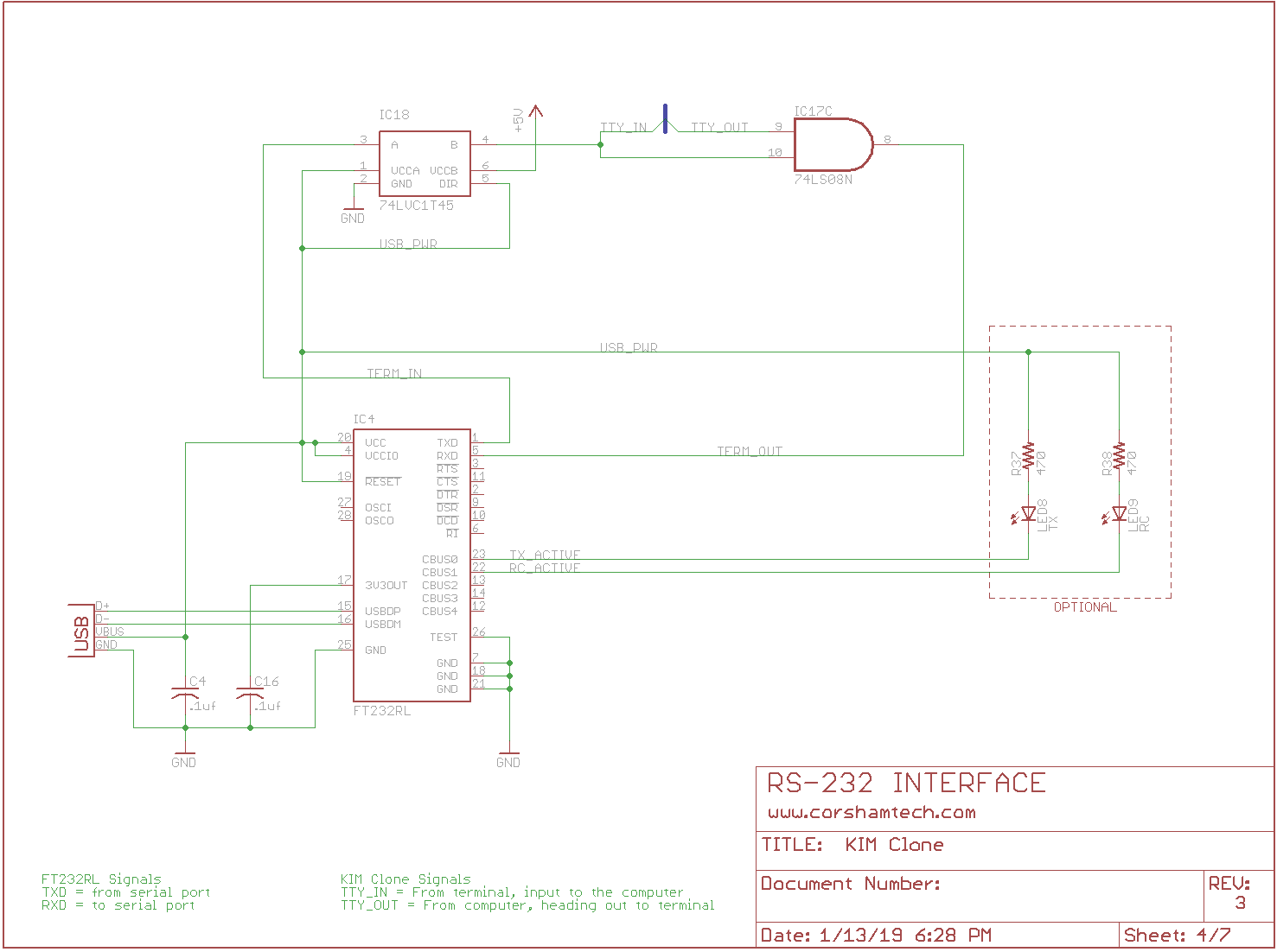
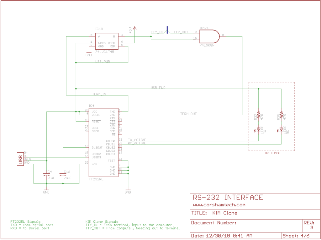
TTY in and out now at TTL level for USB to TTL converter
TTY PTR and KYBD, +1wV, AUDIO OUT LO not connected
This means, even if the edge to pin connector issue is solved, the standard KIM-1 I/O boards will not work for TTY and audio.
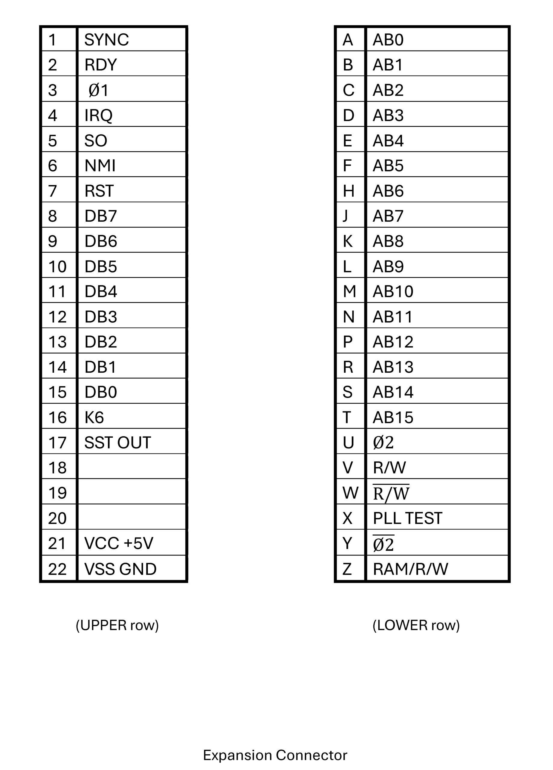
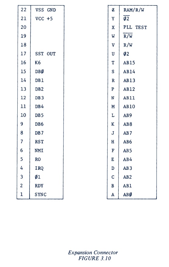
The expansion connector is identical to the KIM-1.
KIM-1 Expansion connector
Power supply
Power has to be applied in the standard KIM-1 manner to the application connector Pin 1 = GND, pin A = 5V. Note that reversing these pins will mean the dead of the PAL-2!
Expansion
As a first suggestion for a PAL-2 extension I see a board connected to Application and Extension connectors with:
Power switch
28C64 (or bigger, switchable in 8K chunks) EEPROM
Connector for the USB to TTL
External power connector, switchable between this and USB to TTL connector
TTY/LED keyboard switch
connector for the Application I/O ports PA0-PB7
Power switch
Optional:
Pin connector for PAL-1 Cassette Interface audio board
The KIM-1 has hardware and software in the 6530-003 ROM to save and dump files on audio tape.
Not used by most KIM clone users, so it is not present on the Corsham KIM Clone and the PAL-2.
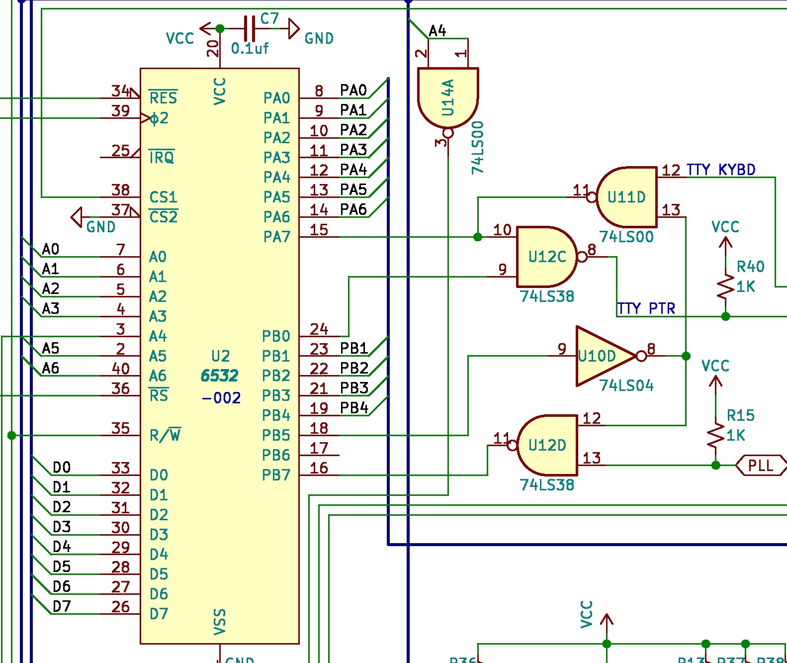
But it is possible to have the audio in/out with one patch wire between pin 11 of U12D and the application connector!
KIM-1 Audio and TTY circuit
PAL-2 Audio and TTY circuit
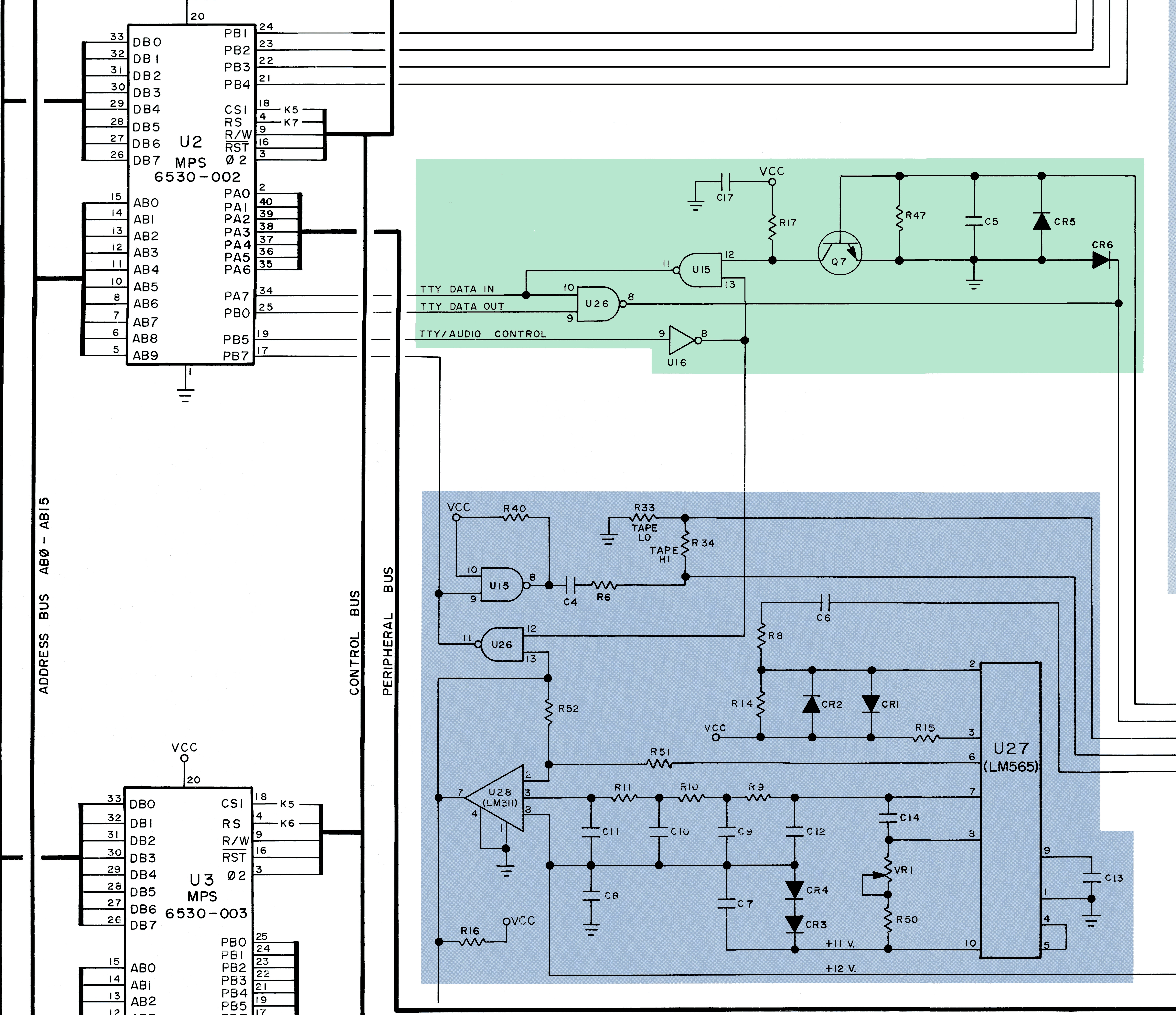
On the KIM-1 circuit you can see the audio I/O is seen by the CPU at pin PB7 of the 6530-003. It is either an input or an output under control of the audio routines in the ROM.
The U26 (also present on the PAL-2 as U12d) is an open collector NAND feding PB7. On one input of U26 is PB5 from the 6530/32 (inverted by U16 (KIM-1_ or U10D (PAL-2), on the other is the output of the audio circuit generating TTL pulses from the audio sound input. This way PB7can be used both as input and output.
The PAL-2 and the KIM-1 has on the extension connector the signal PLL(_TEST), which is connected to U126/U12D. This is on the KIM-1 the output of the audio circuit.
So we have audio in (at TTL level) on the PAL-2 covered!
Audio out is available at PB7 at TTL level. With a patch wire between PB7 (or pin 11 of the U12D) to the application connector.
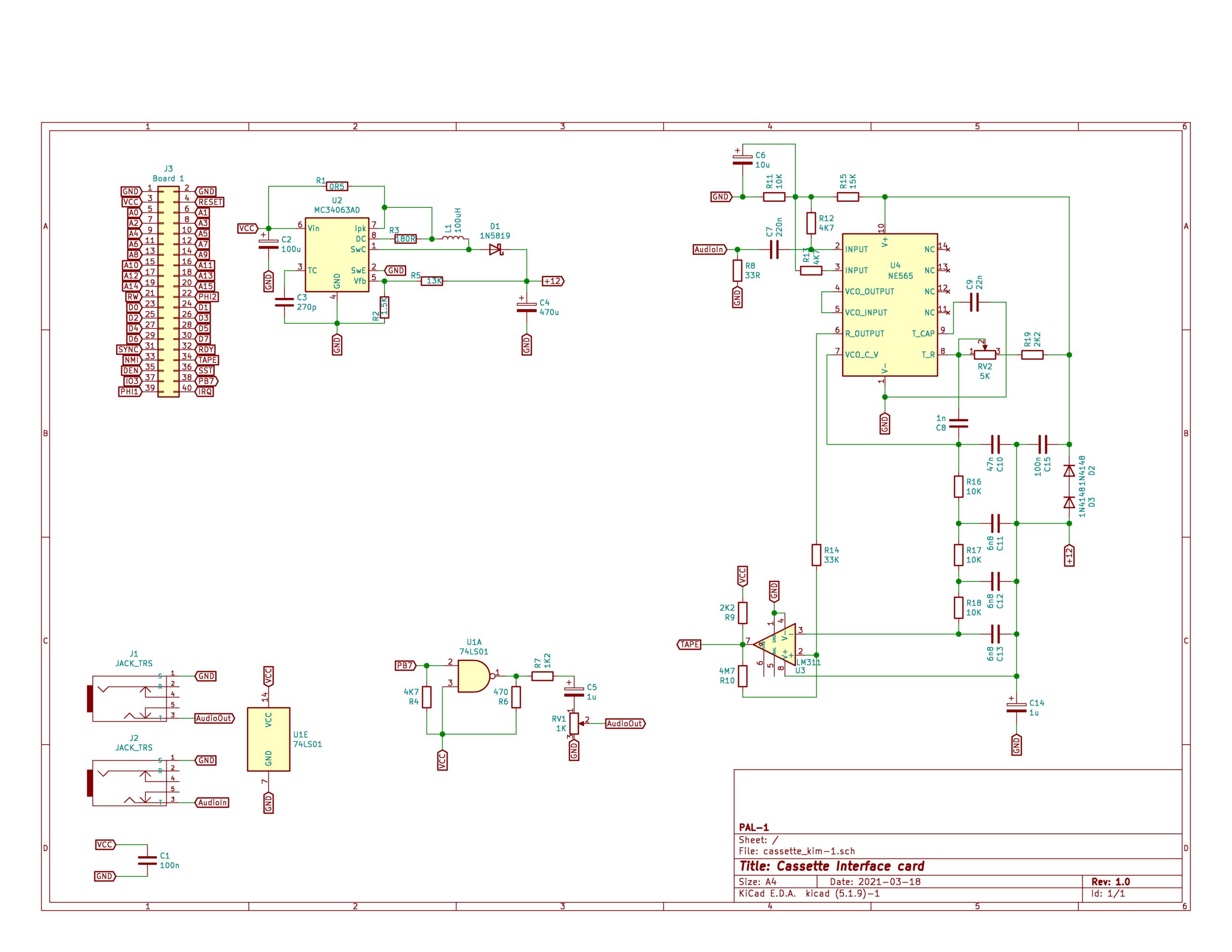
With the PAL-1 Cassette interface we can have the PAL-2 read and write KIM-1 audio cassette files this way. PLL_TEST to TAPE and a wire from PB7 to PB7 is all you need to connect to the Cassette Interface (and GND and +5V ofcourse).
Leaving R9 out of the Cassette Interface may be a good idea, there is already a pullup in the PAL-2 of 1K.
Physical Dimensions
The connector on the PAL-2 is a 2.54 mm pitch 2×22 female pin header connector.
The dimensions of the PAL-2 PCB are 168 mm x 218 mm.
Next two images show the connector, first shows the distance between the two connectors, while the second shows the distance from the PCB edge to the connector’s outer side.
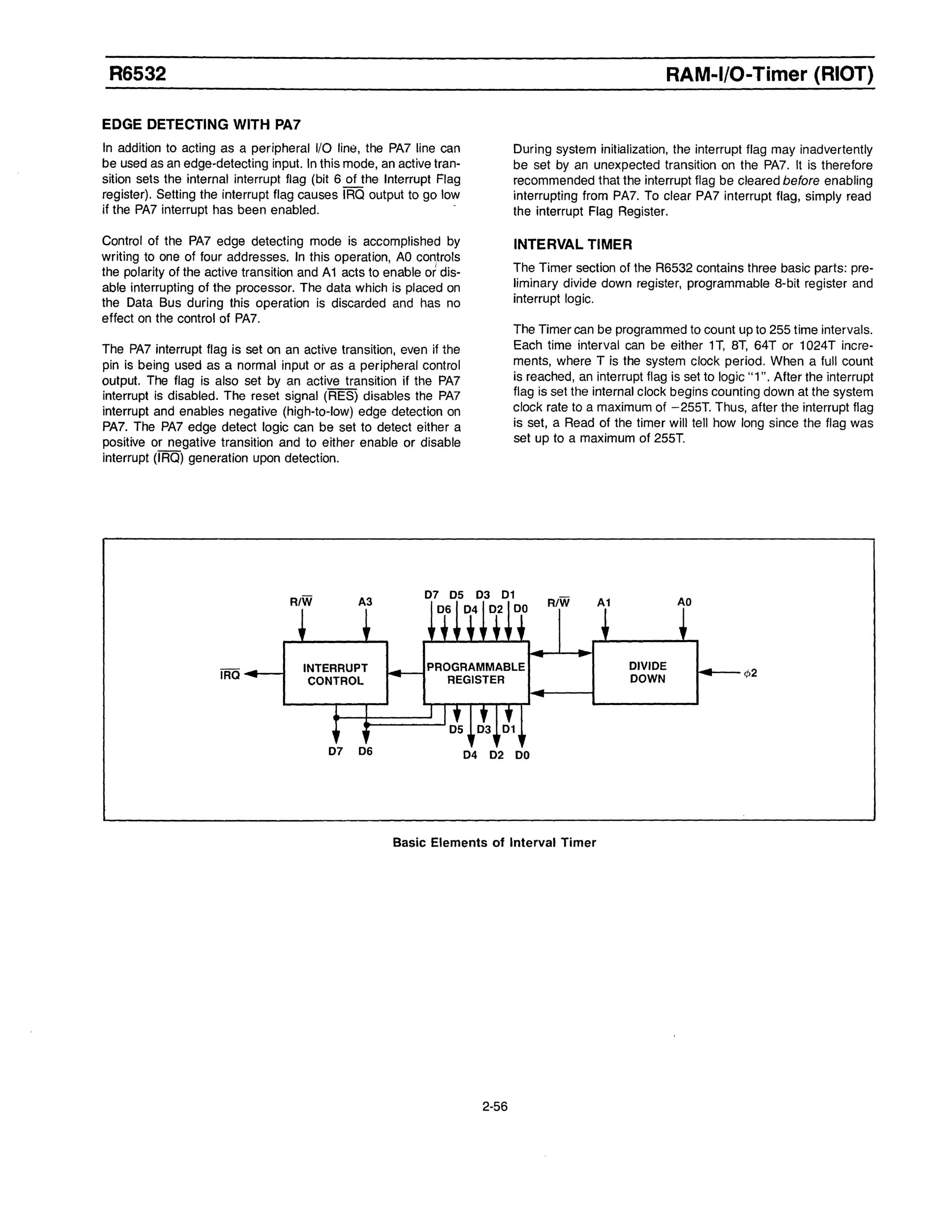
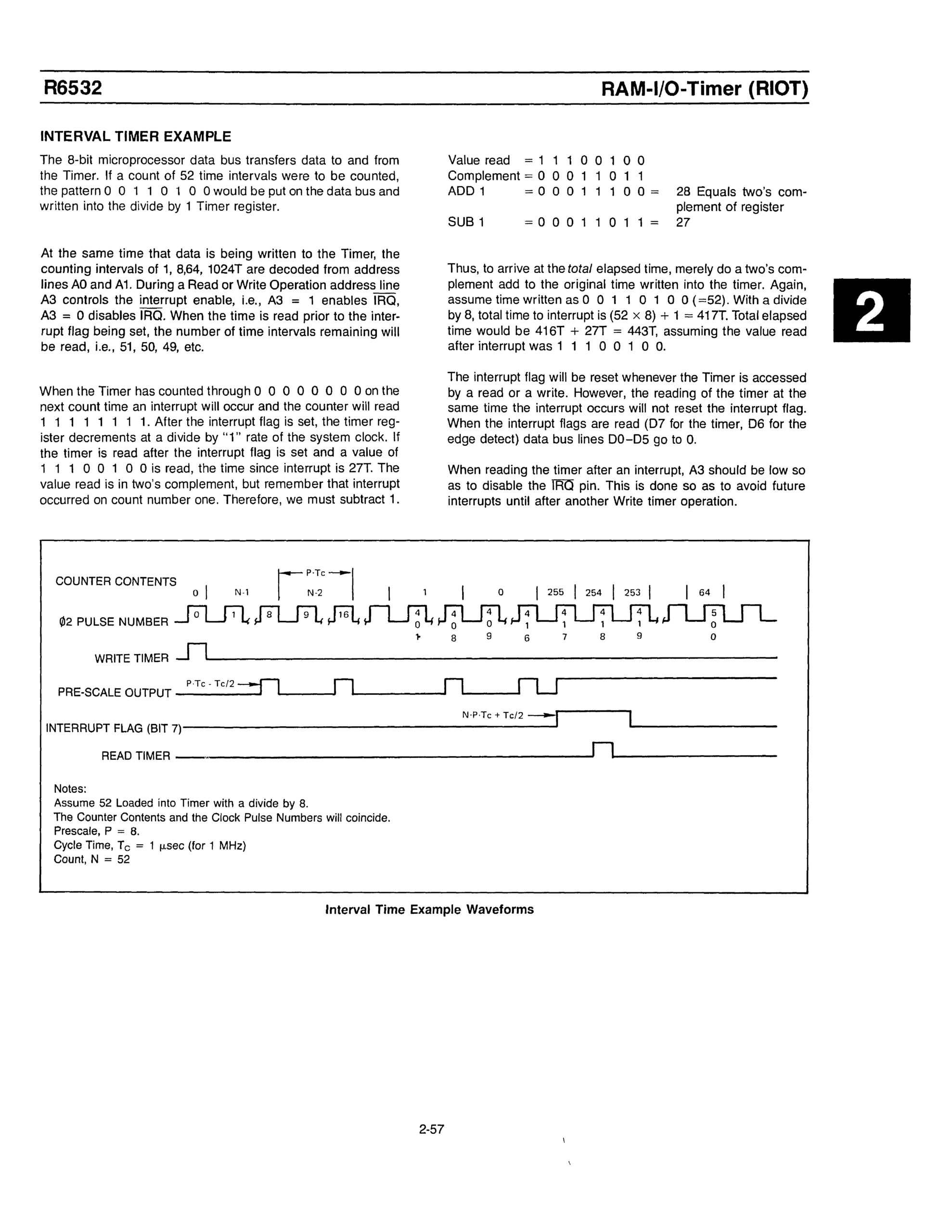
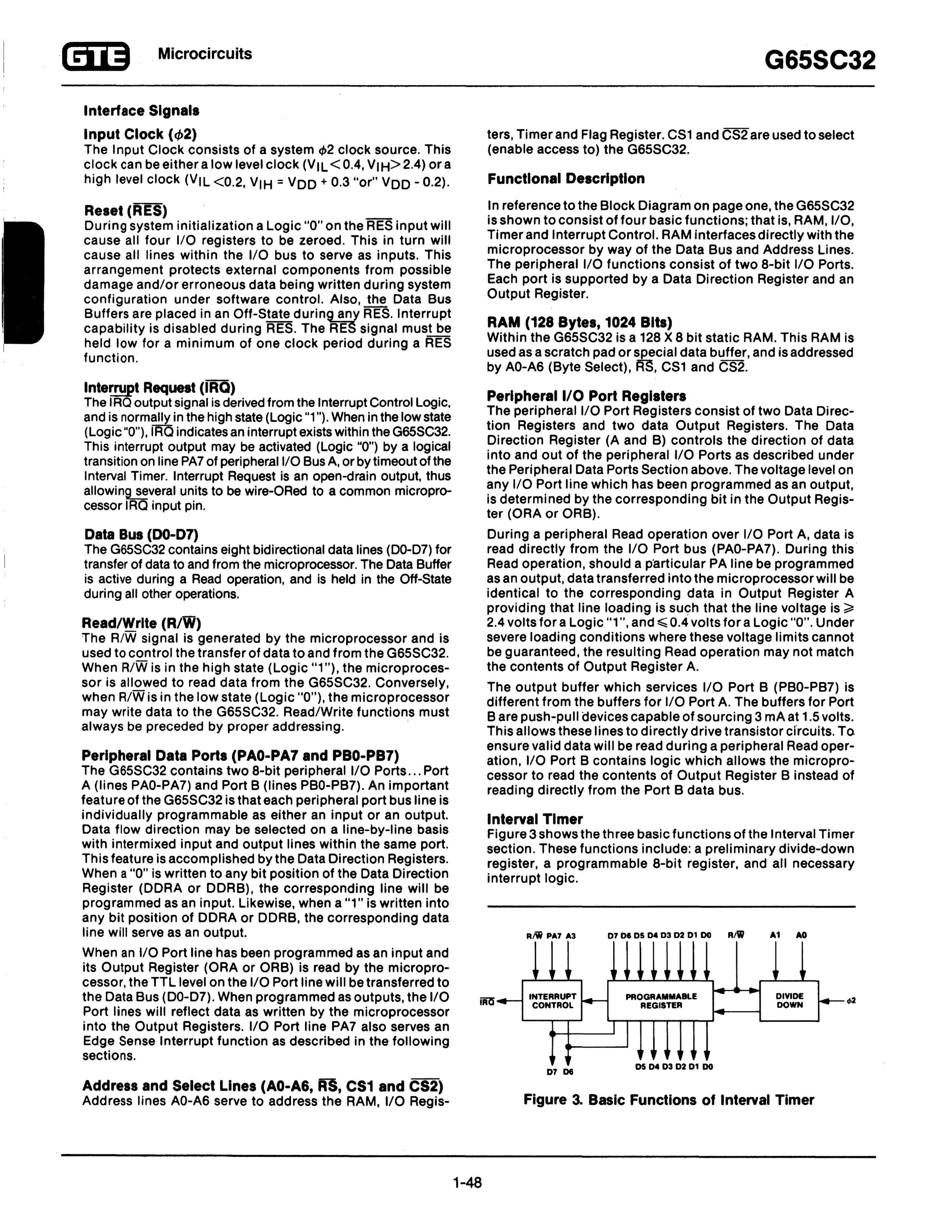
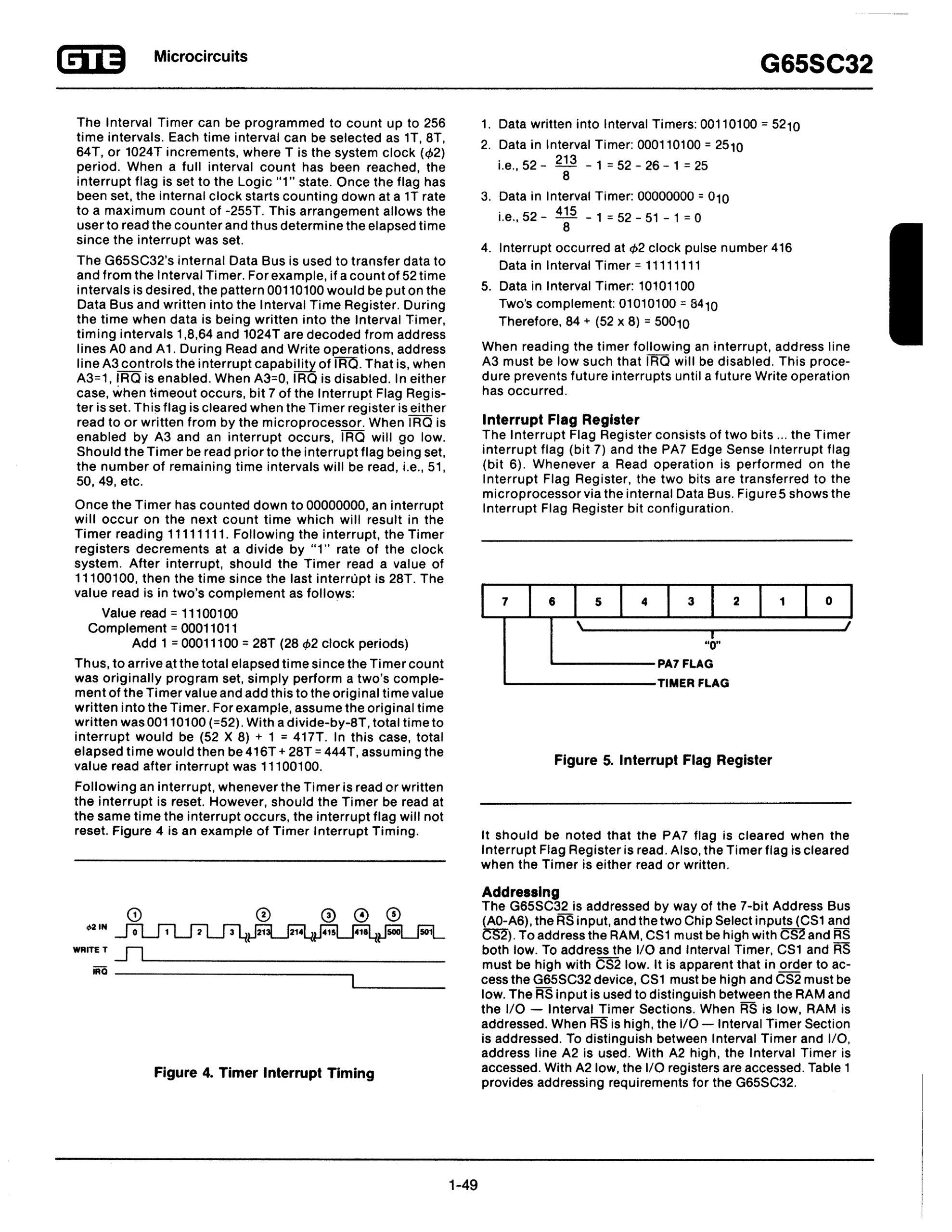
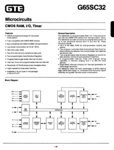
There is a subtle difference between the NMOS 6532 and the CMOS G65SC32 datasheet regarding the timer of 1 in elapsed time.
It is in the paragraph starting at ‘Once the time has counted down to 00000000, an interrupt will occur ….’
On the 6532 that takes 27T (T is the clock tick), on the G65SC32 28T.
That makes in the example the total elapsed time 443T on the 6532 and 444T on the G65SC32.
Look at these pages about the timer from the datasheets of the R6532 and 6G5SC32 (see below and here)
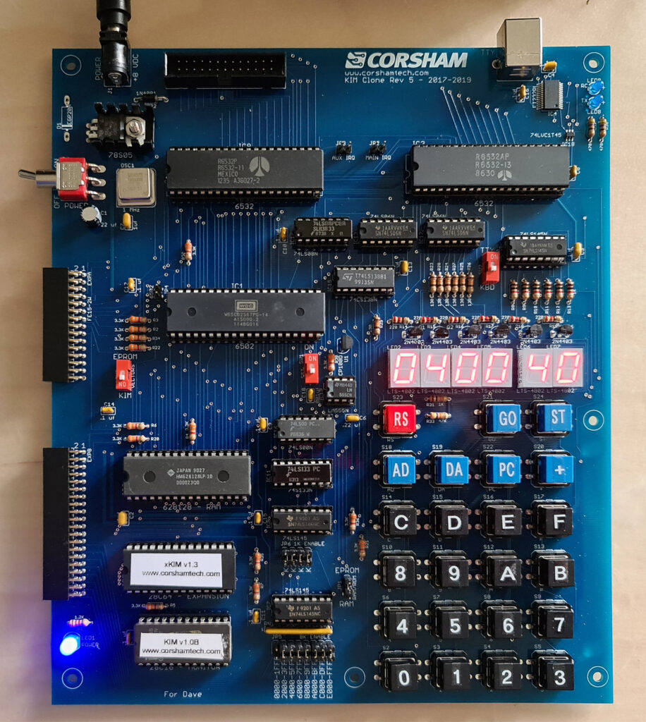
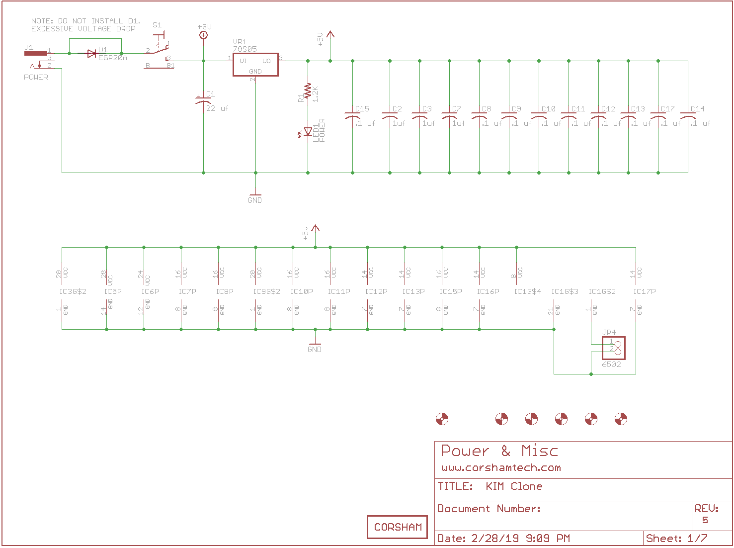
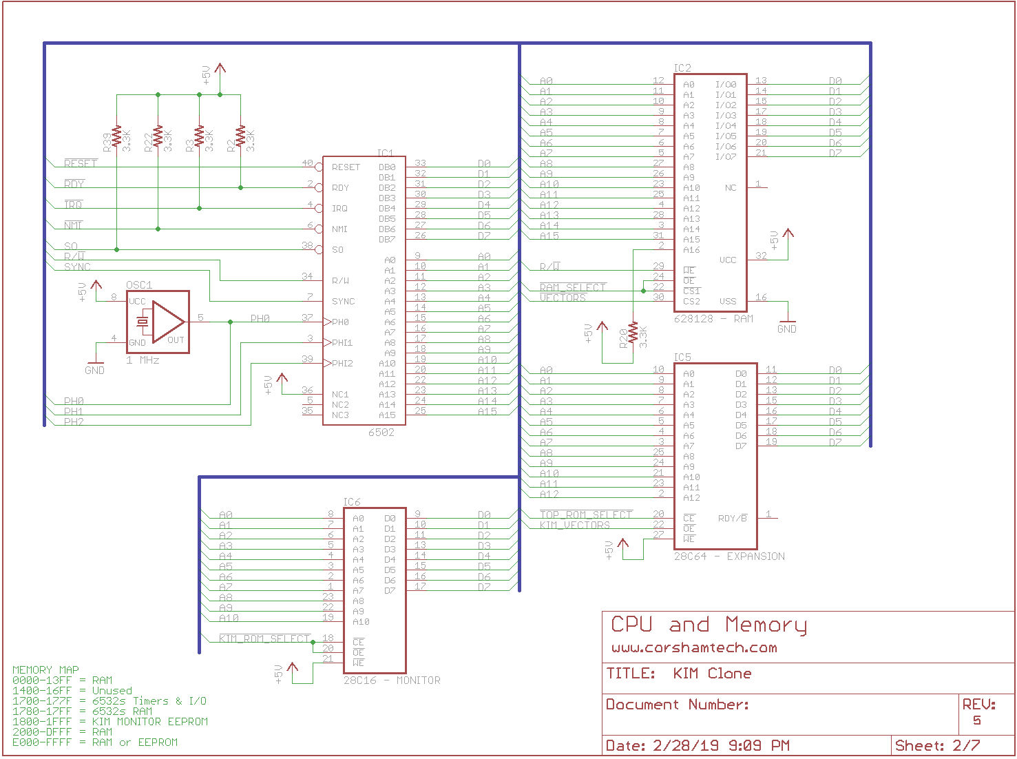
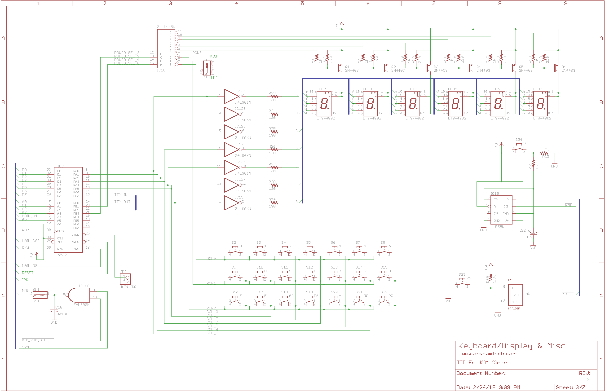
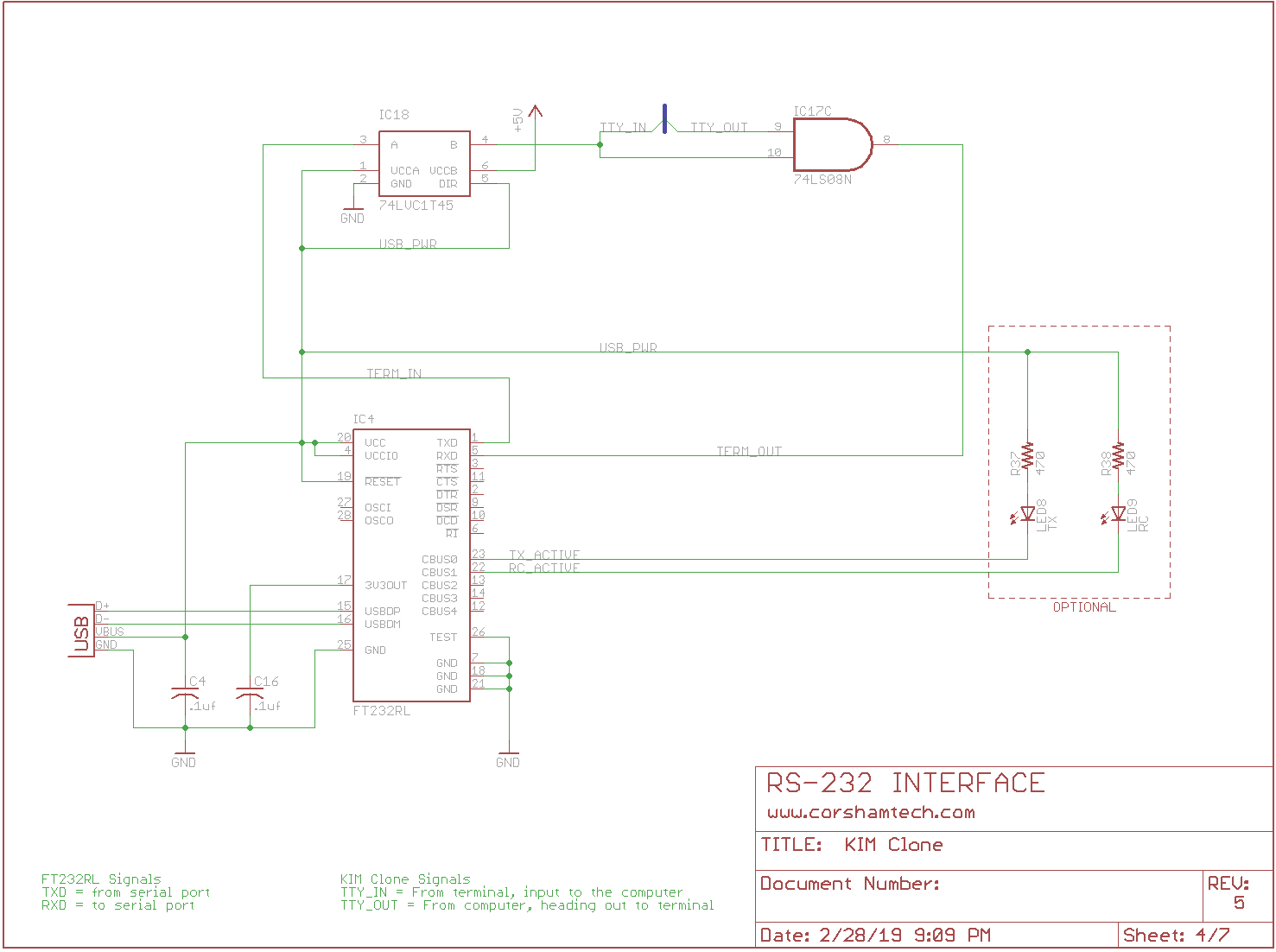
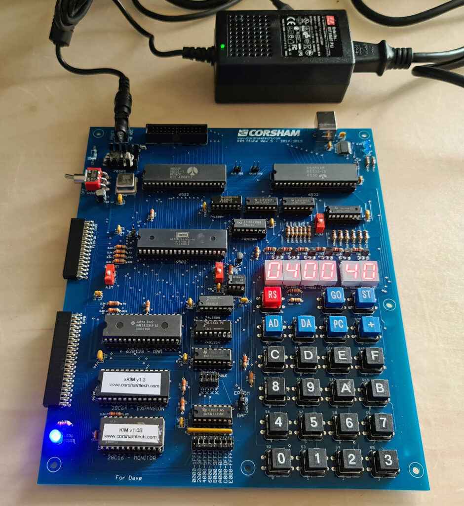
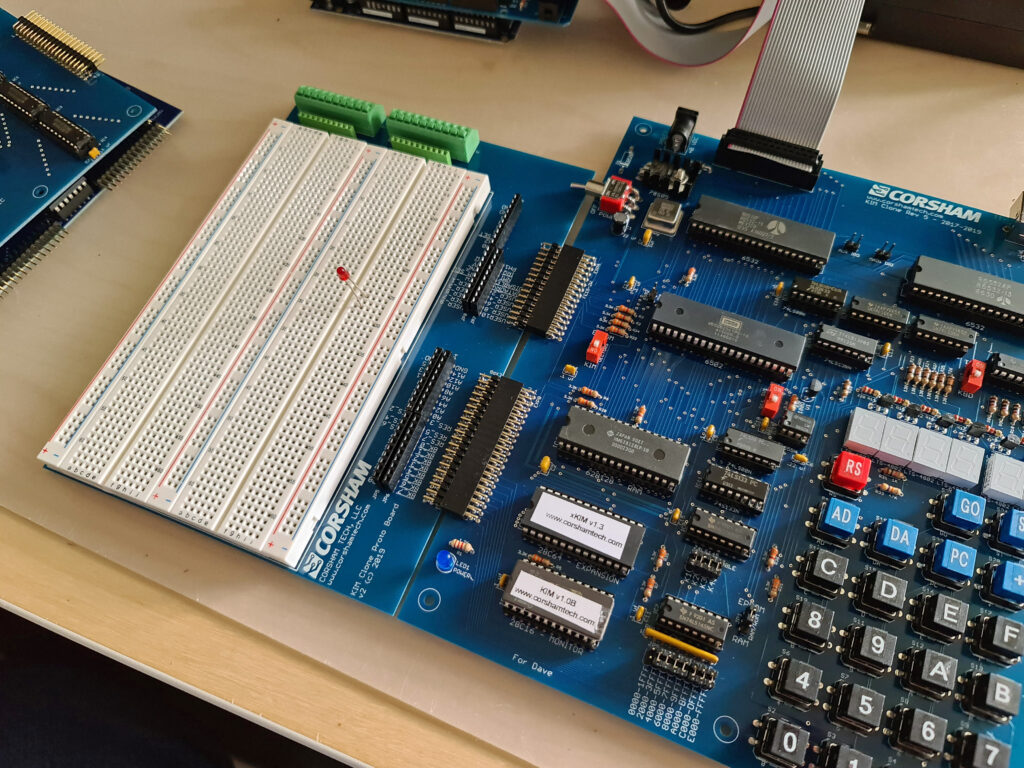
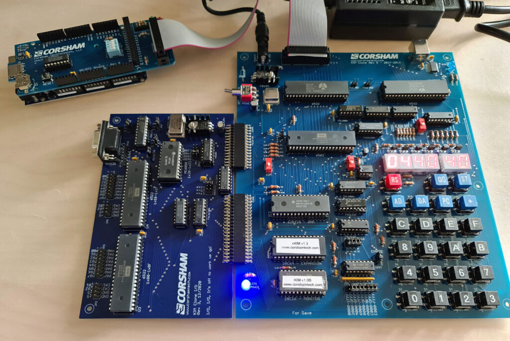
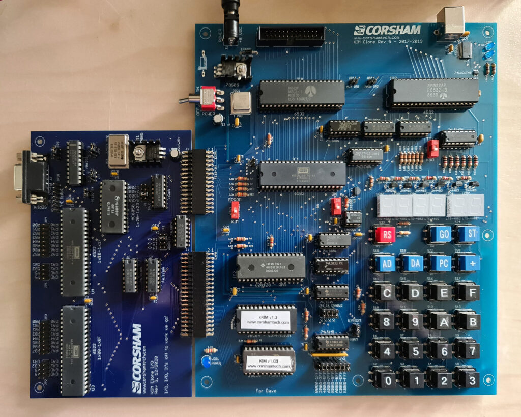
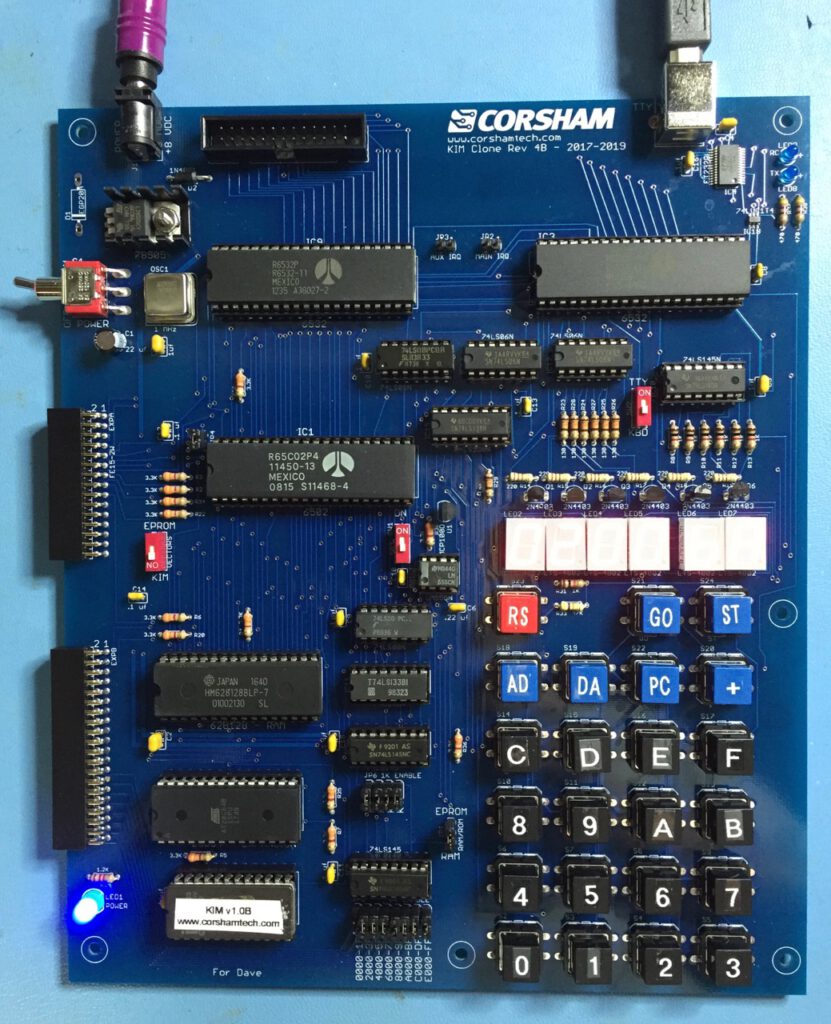
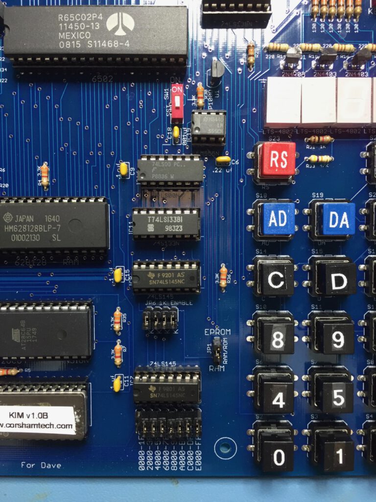
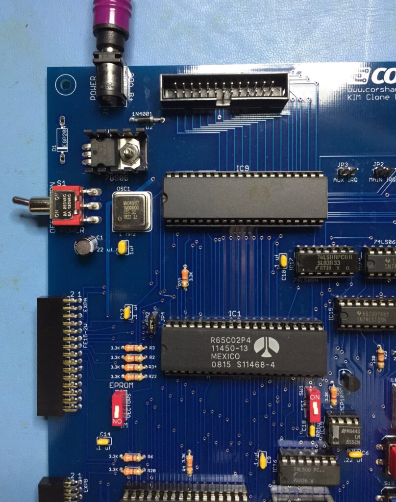
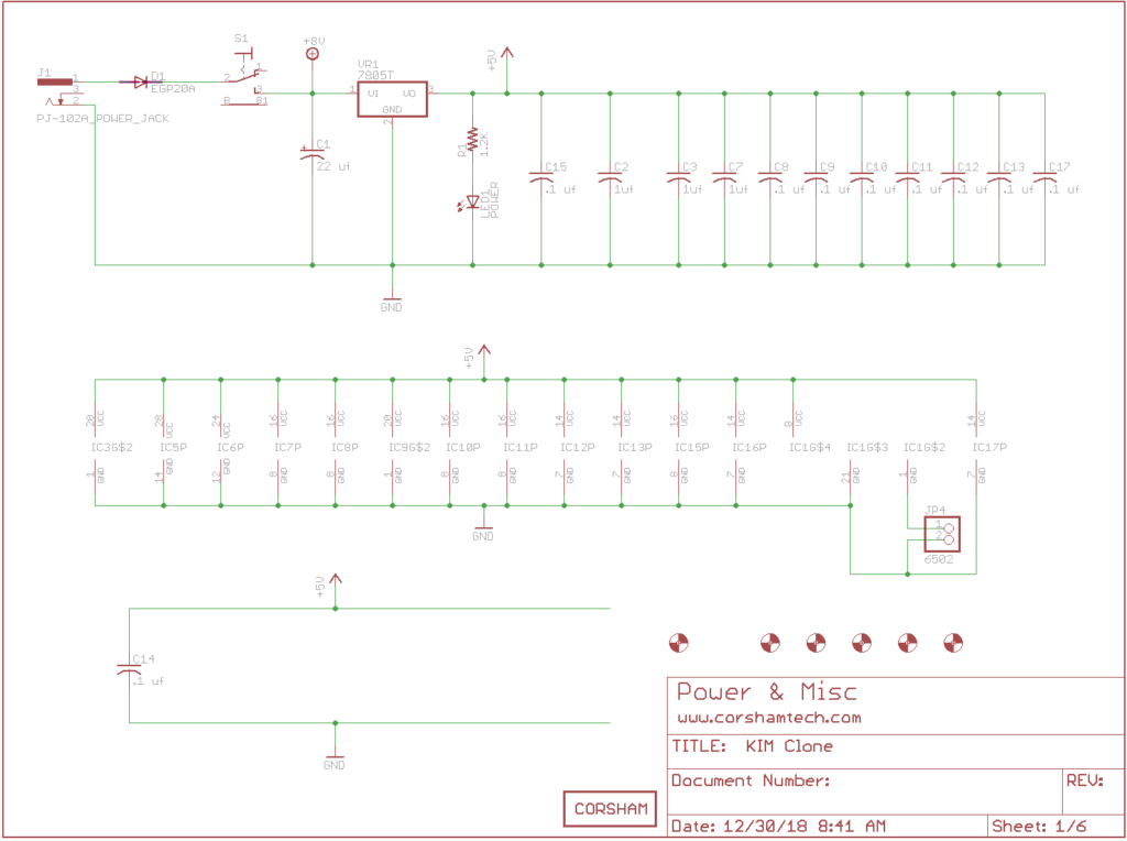
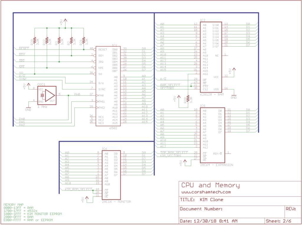
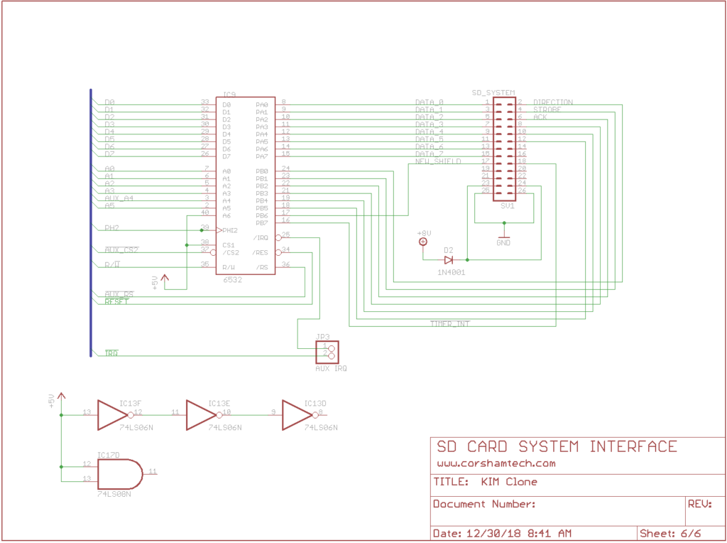
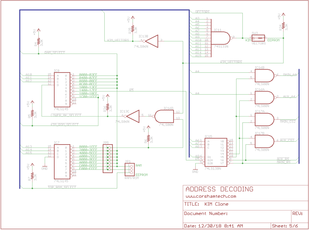
After almost a year (2019)of on-again, off-again, development we finally have a new revision of the KIM Clone.
It has everything the previous versions have, but with a few improvements people have asked for (or I wanted):
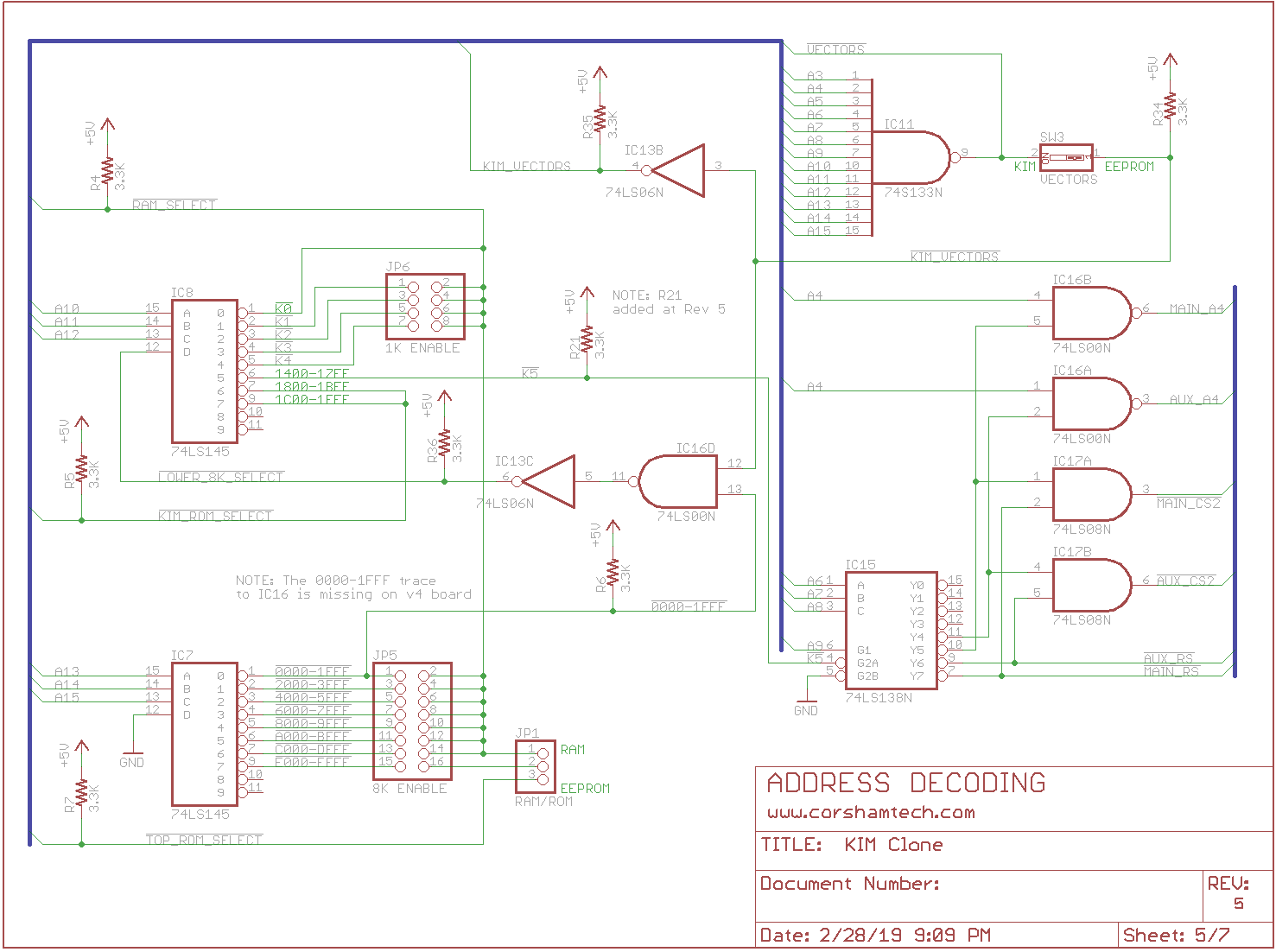
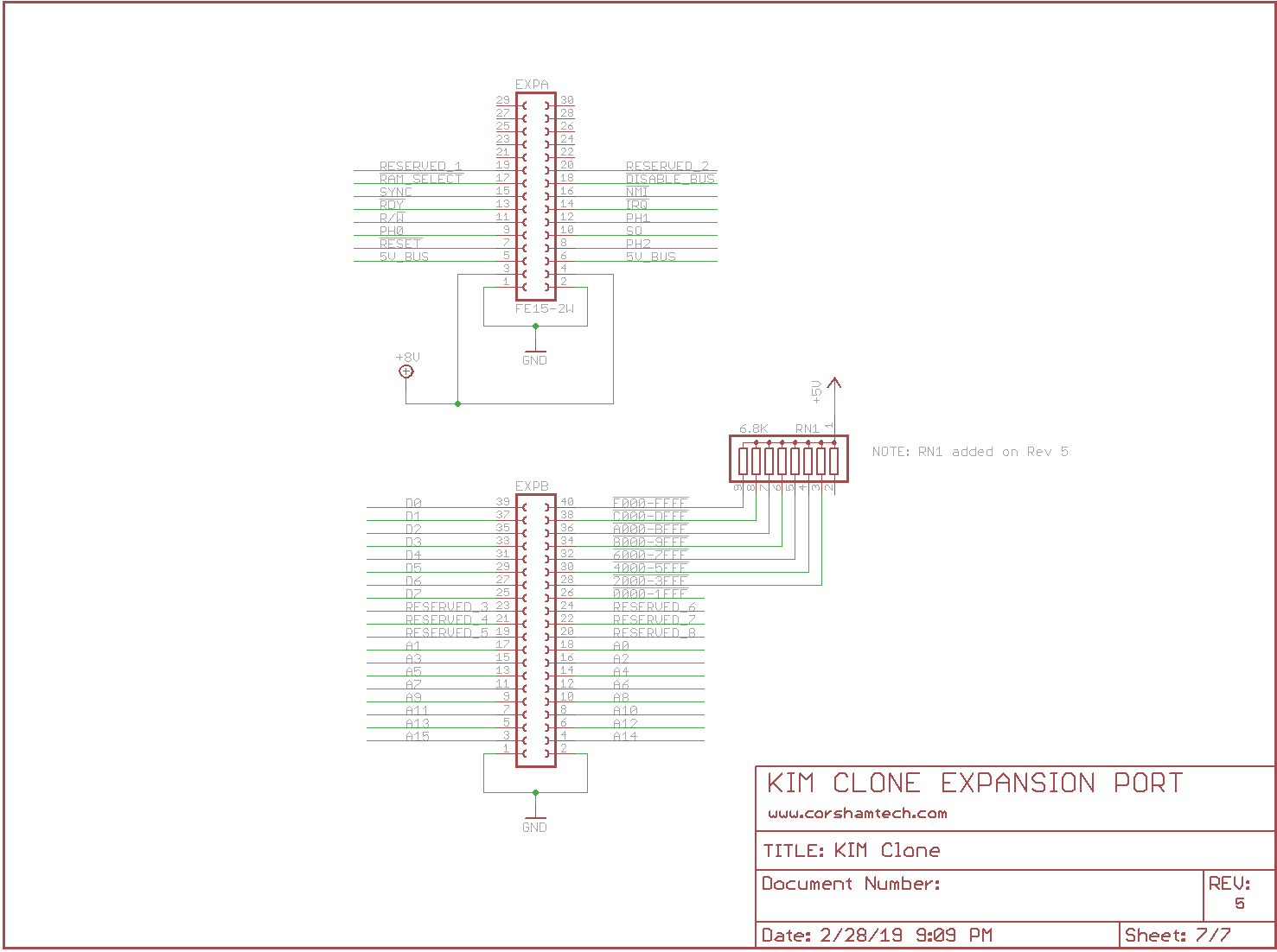
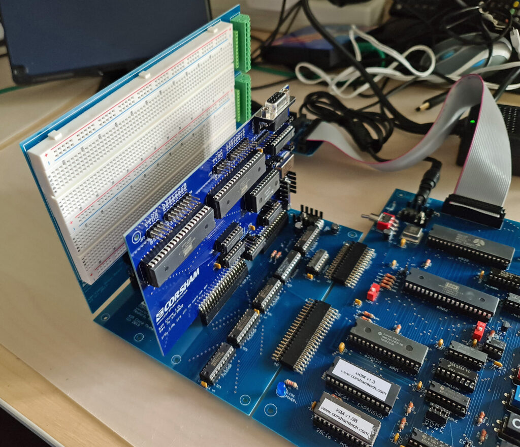
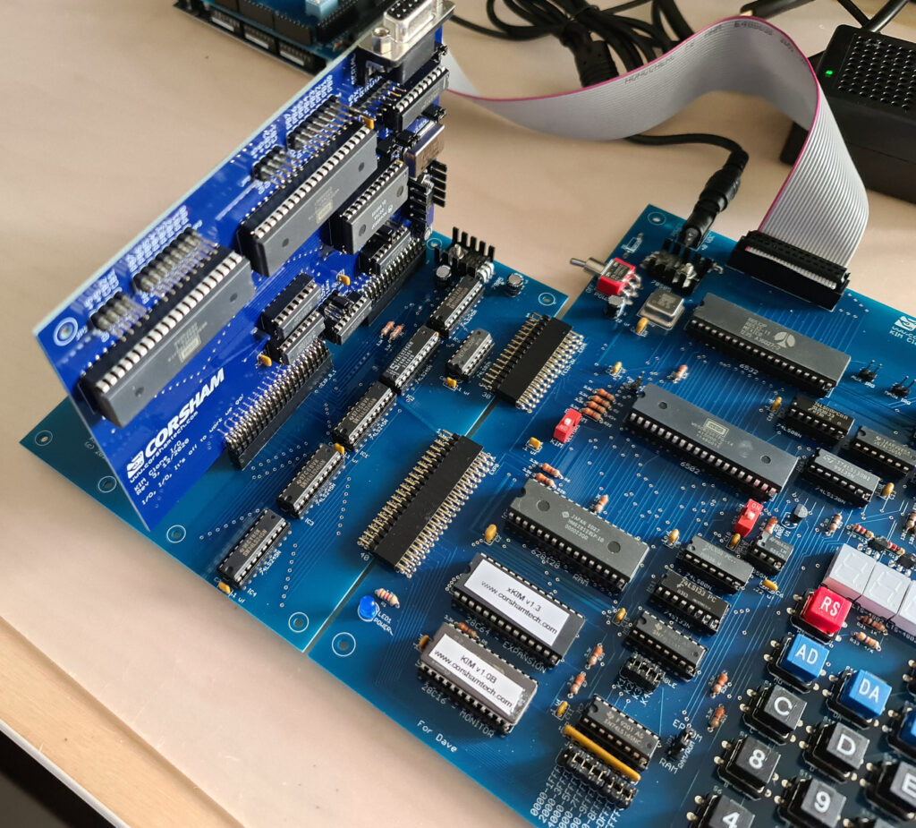
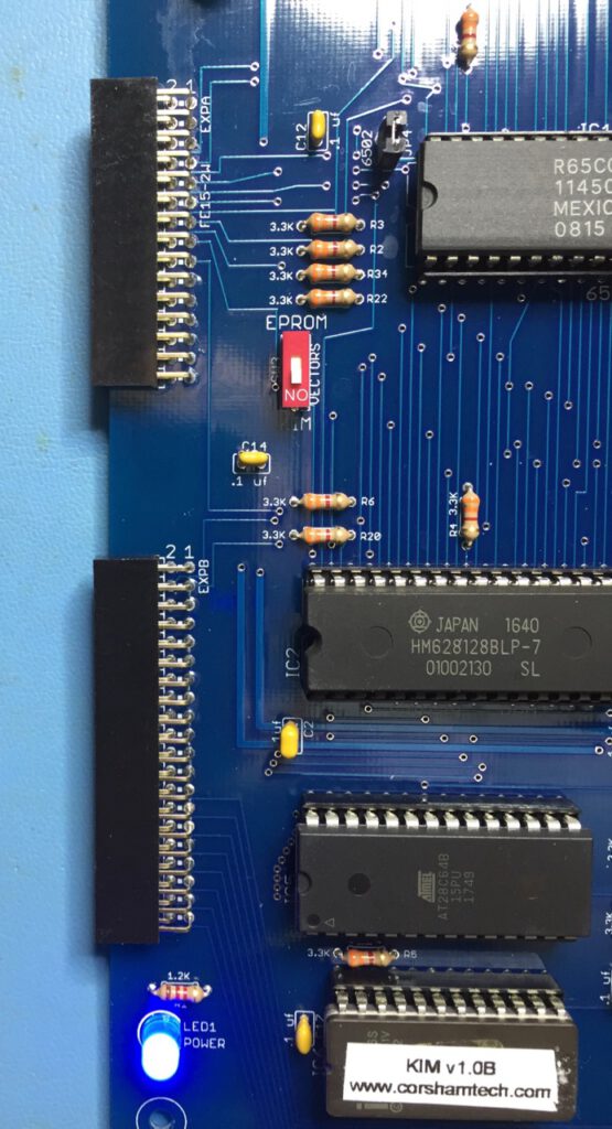
Expansion bus connectors! This was widely requested. Includes most processor signals, address and data buses, along with bank decoding lines. This is intended to plug into either a prototype board (more on this later) or a motherboard (in the works).
More jumpers to enable/disable blocks of RAM from being decoded. K1-K4 each have jumpers, and 8K blocks for the entire memory map have another set of jumpers. This allows blocks to be disabled on-board, then mapped to a user-supplied circuit.
Power on reset. Not a major feature, but I didn’t like having to press RS every time I turned on my KIM-1.
Power connector and the power switch moved to the top edge of the board.
Revision 3 boards had a number of minor changes to fix know issues on Revision 2 boards. No new features or capabilities were added.
– IC19 was removed
–IC18 changed from 74AVC1T45 to 74LVC1T45
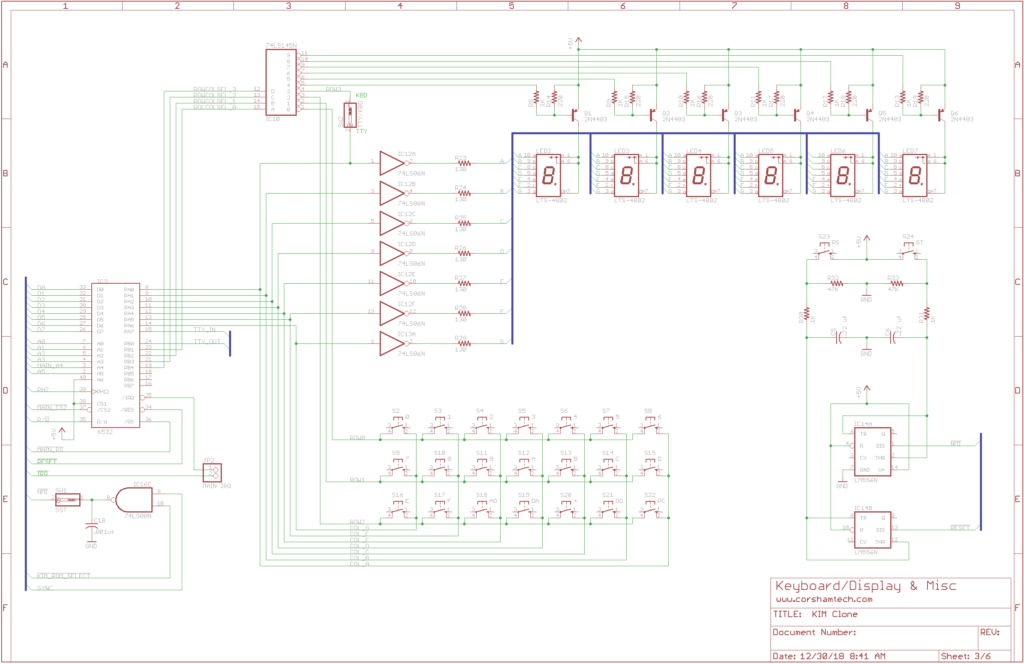
– IC16 changed to 74LS00
– IC7 and IC8 changed to 74LS145
– R37 and R38 changed to 470 ohms
– C18 was added
– IC17 had power routing fixed
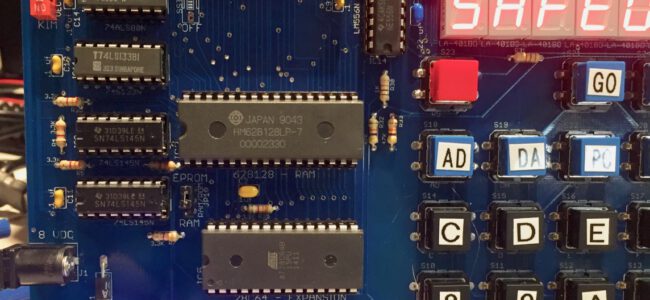
In 2017 Bob Applegate started to design a KIM CLone.
He went to 5 versions.
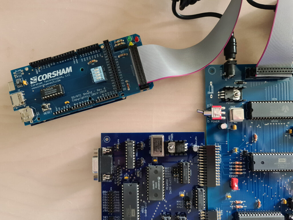
The first were enhanced KIM-1 replica’s without expansion connectors but with lots of RAM and ROM. The later versions and 5 did have expansion connectors, and a Motherboard, I/O board and Protoboard were added.