
Christian Ortner (mister-freeze at the VzEkC e. V. forum build a SBC with expansion around a TIM IC.
Here is his projects description of the TIM-1 SBC.
Text by Christian:
Since the TIM chip is actually not available, the TIM-1 is unfortunately only useful for people who are in possession of a 6530-004. But, there is still the TIM-2 😉 The idea for the project came up when I got a few MPS 6530-004 by chance. Actually I always wanted to have an affordable KIM-1, but so far I haven’t found one. I also wanted to learn how to use KiCad.
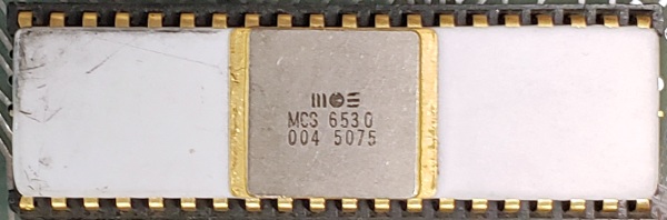
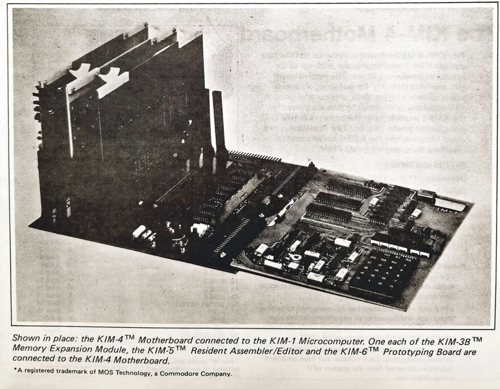
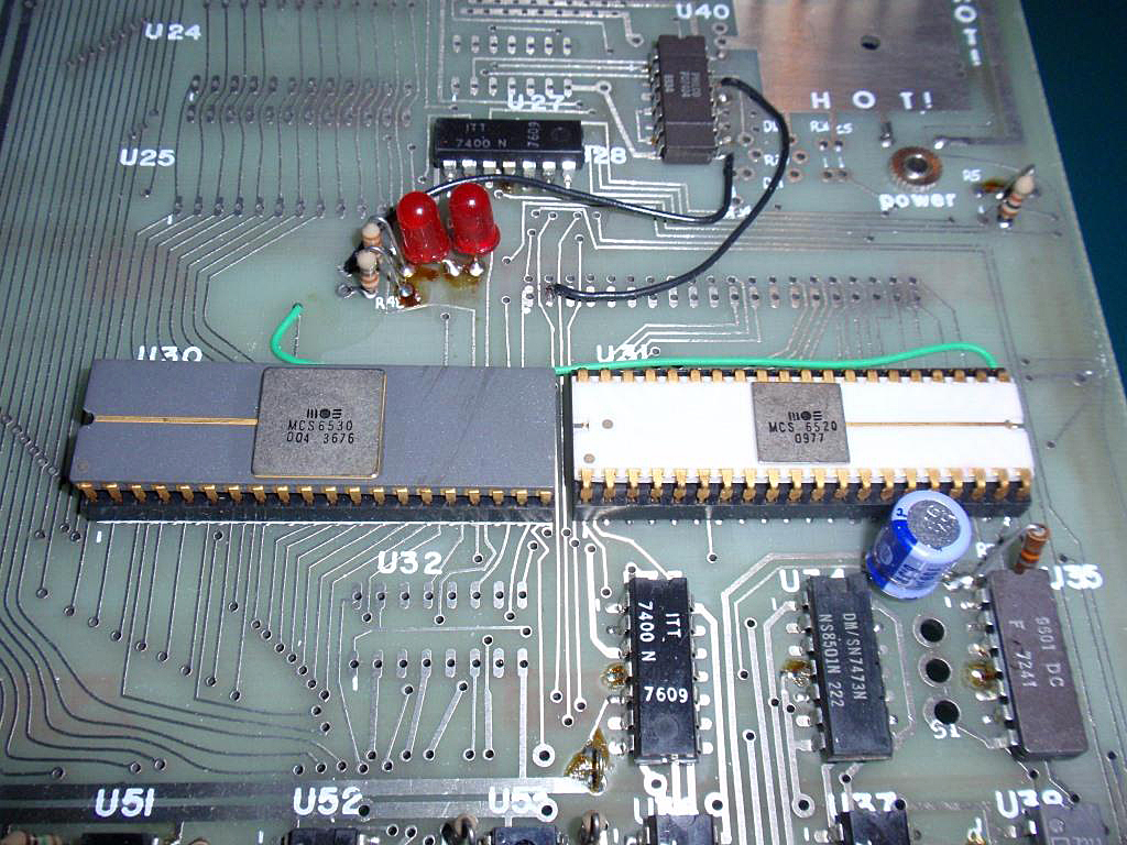
The RRIOT 6530-004 (TIM chip) was sold by MOS only as a kit in the form of the TIM chip, a manual and a schematic. This meant that the computer enthusiast or developer had to assemble the rest of the system themselves. Commercially, the TIM chip was probably only used in the Jolt and Super Jolt. It was not until the KIM-1 that MOS released a complete development and learning system.
TIM-1
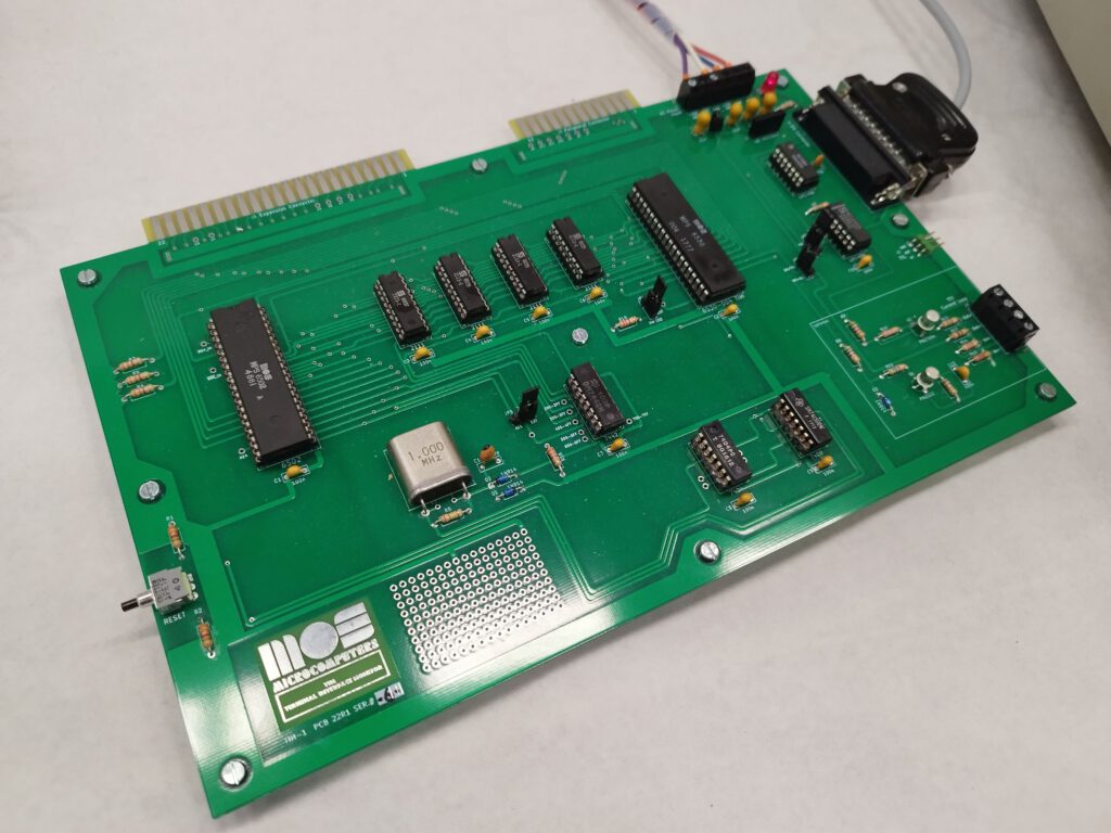
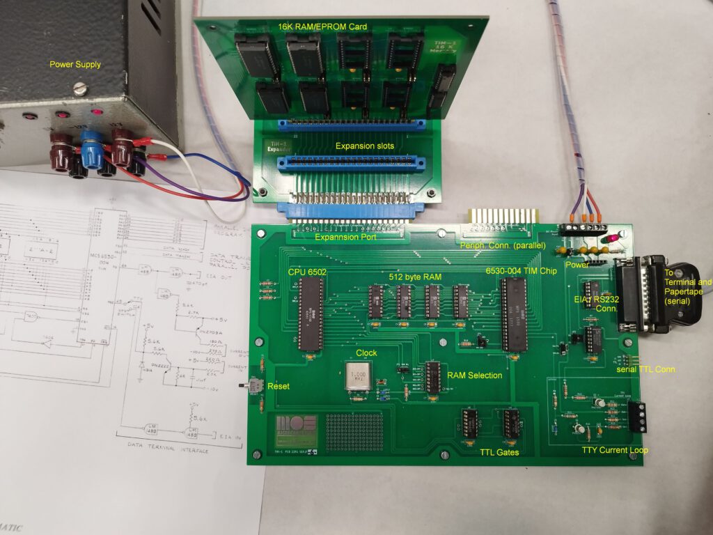
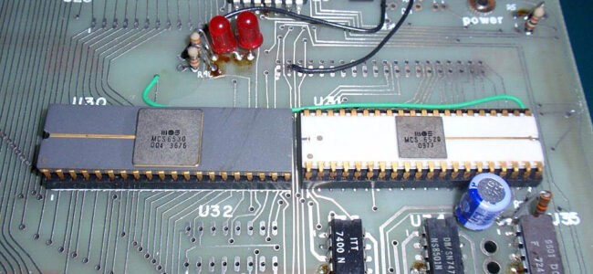
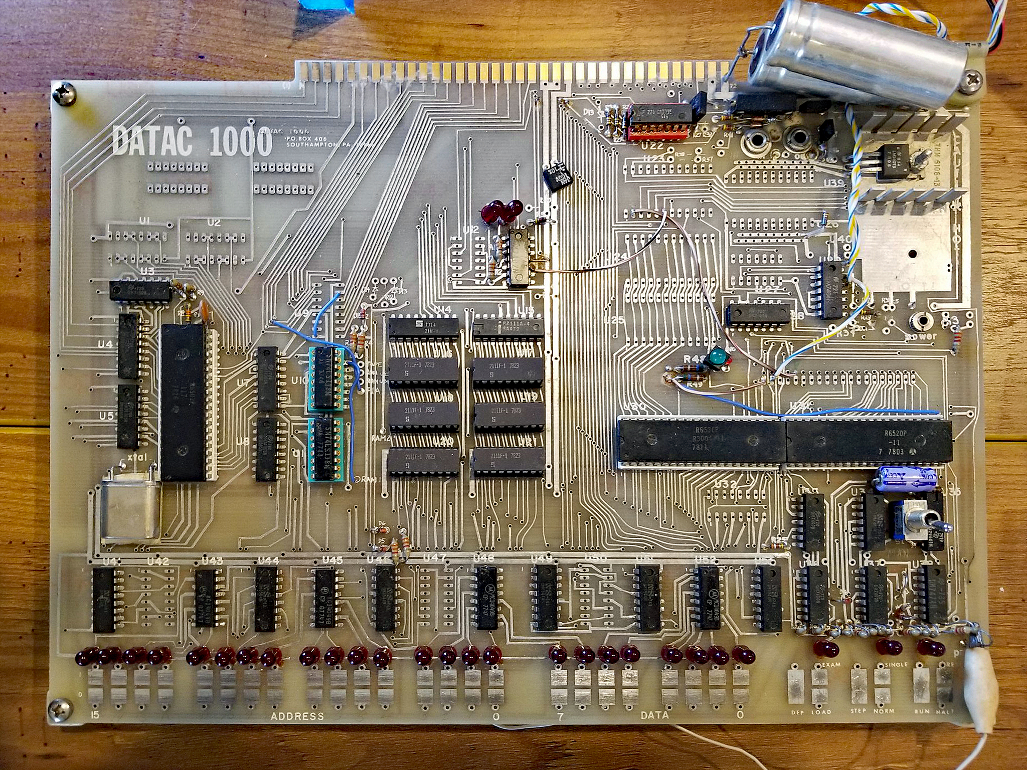
With the TIM-1 project a SBC should be created, as authentic and as exact as possible after the original circuit diagram for the TIM chip of MOS. So for the TIM-1 -at least for the mainboard- only those parts should be used which were included in the MOS schematic and by the way only those parts which were available in the mid seventies. The design is based on the KIM-1 and other SBCs from that time. The layout is adapted to the original schematic, i.e. the parts can be found at the same place where they are placed in the schematic. This makes it easy to understand the system from the schematic. The TIM-1 needs 5 V supply voltage. If you use the EIA (RS232) interface, you have to supply -12V and +12V additionally. For the current loop (Teletype) there is an additional -10V supply required, but it can be assumed that -12V is also possible (maybe a Resistor must be changed). The transistor -according to the original schematic- PN2709A is probably a typing error. The PN 2907A will surely be the correct one. For simplified use with a modern terminal emulator the serial interface is led out laterally as TTl level. This allows the system to operate using only 5V and a USB to TTL adapter. The address decoding for the selection of RAM and RRIOT is incomplete, therefore there is a multiple selection over the whole address range. Therefore, when using the expansion card, an external disabling line for the internal RAM and the TIM chip is necessary to avoid address overlaps. Surely this could have been improved right away, but the TIM-1 should be expandable but, as far as possible, conform to the plan of MOS. The 4 SRAMs 2111 (256×4) on the board provide the user with 512 bytes (page 0 and 1). For small programs and for getting to know the TIM-1 this is very sufficient, but for more extensive programs this is of course too little. Therefore, the TIM-1 has received a simple memory expansion. This external card can be equipped with 8 pieces of RAM or EPROM (probably also modern EEPROM) with standard 2k x 8 (e.g. 2016 RAM and 2716 Eprom). A 4kx8 EPROM 2732 can be used as well, here the upper or lower 2 kB must be selected by jumper.
The operation of the TIM-1 is almost completely covered with the TIM manual from MOS.
Since the TIM chip is actually not available, the TIM-1 is unfortunately only useful for people who are in possession of a 6530-004. But, there is still the TIM-2 😉 The idea for the project came up when I got a few MPS 6530-004 by chance. Actually I always wanted to have an affordable KIM-1, but so far I haven’t found one. I also wanted to learn how to use KiCad.
TIM-1 Overview
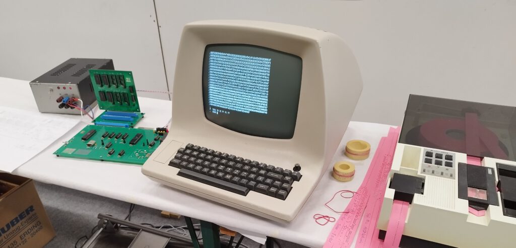
TIM-1 Setup with Terminal and Papertape
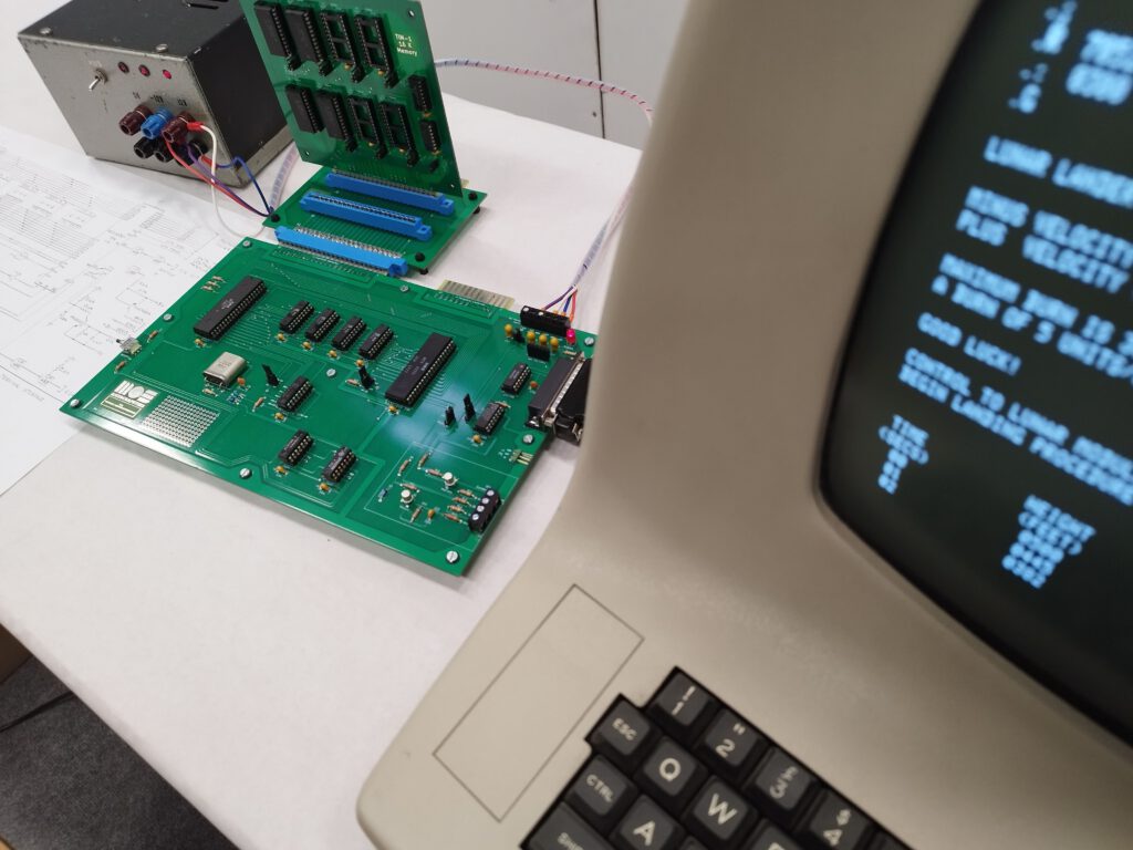
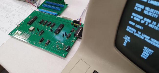
TIM-1 running Lunarlander
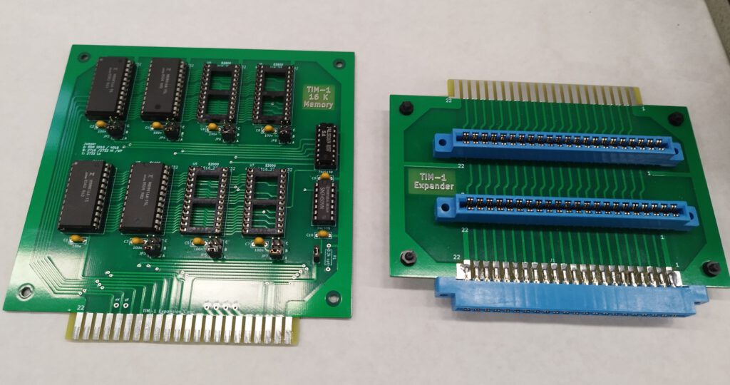
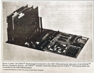
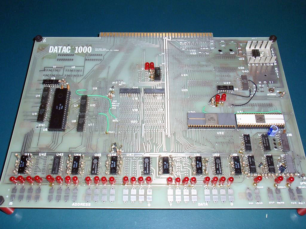
TIM 1 Memory and Slot Card
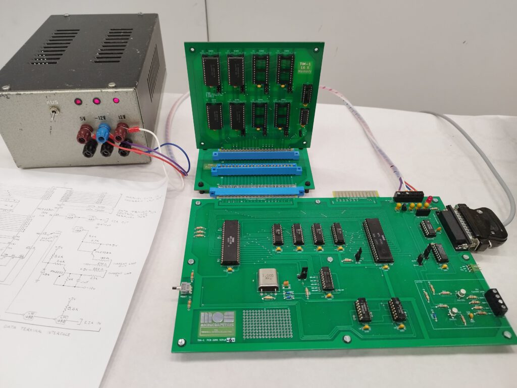
TIM-1 with Expansion
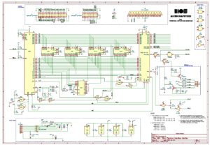 |
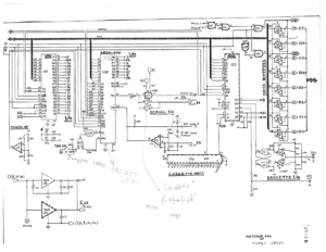
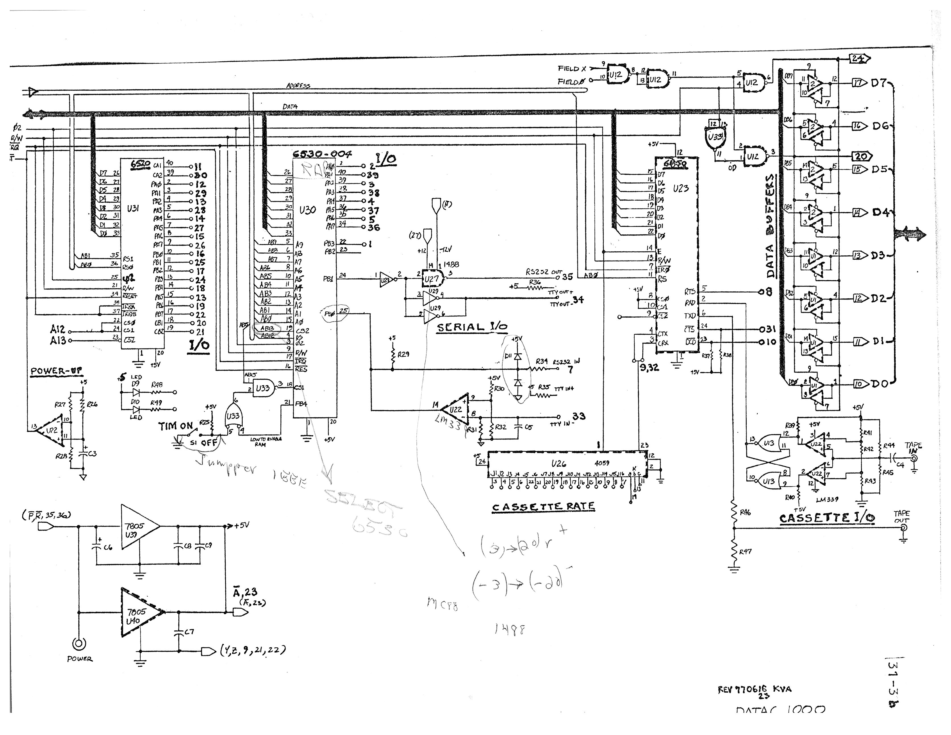
TIM-1 Schematic |
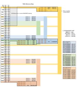 |
TIM-1 Memory MAP |
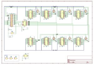 |
TIM-1 Memory Expansion Card |
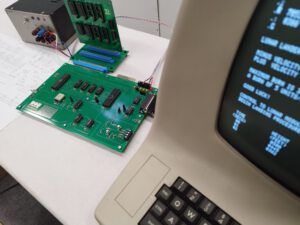 TIM-1 running Lunarlander |
LUNARLANDER for 6502 and TIM |
LUNAR LANDER for the 6502
HEX File from Mark Garetz´s Listing in Dr. Dobb´s Journal (August 1976).
Just typed in with a little debugging by Christian Ortner in 2023
