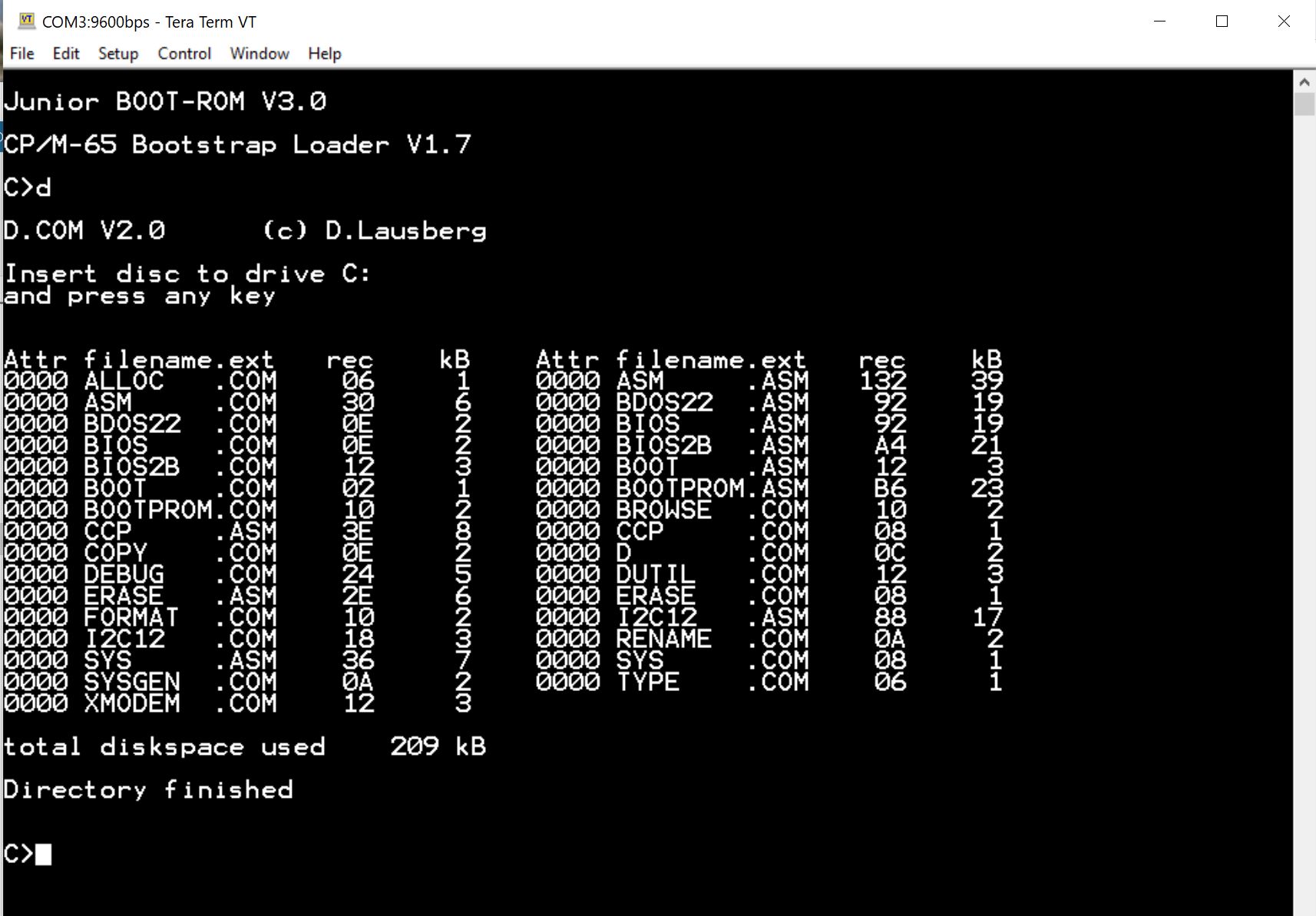
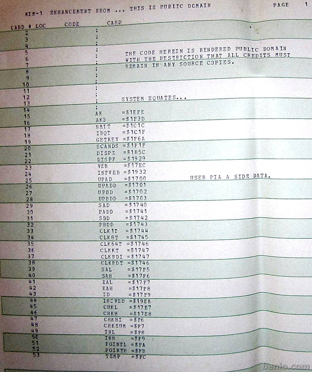
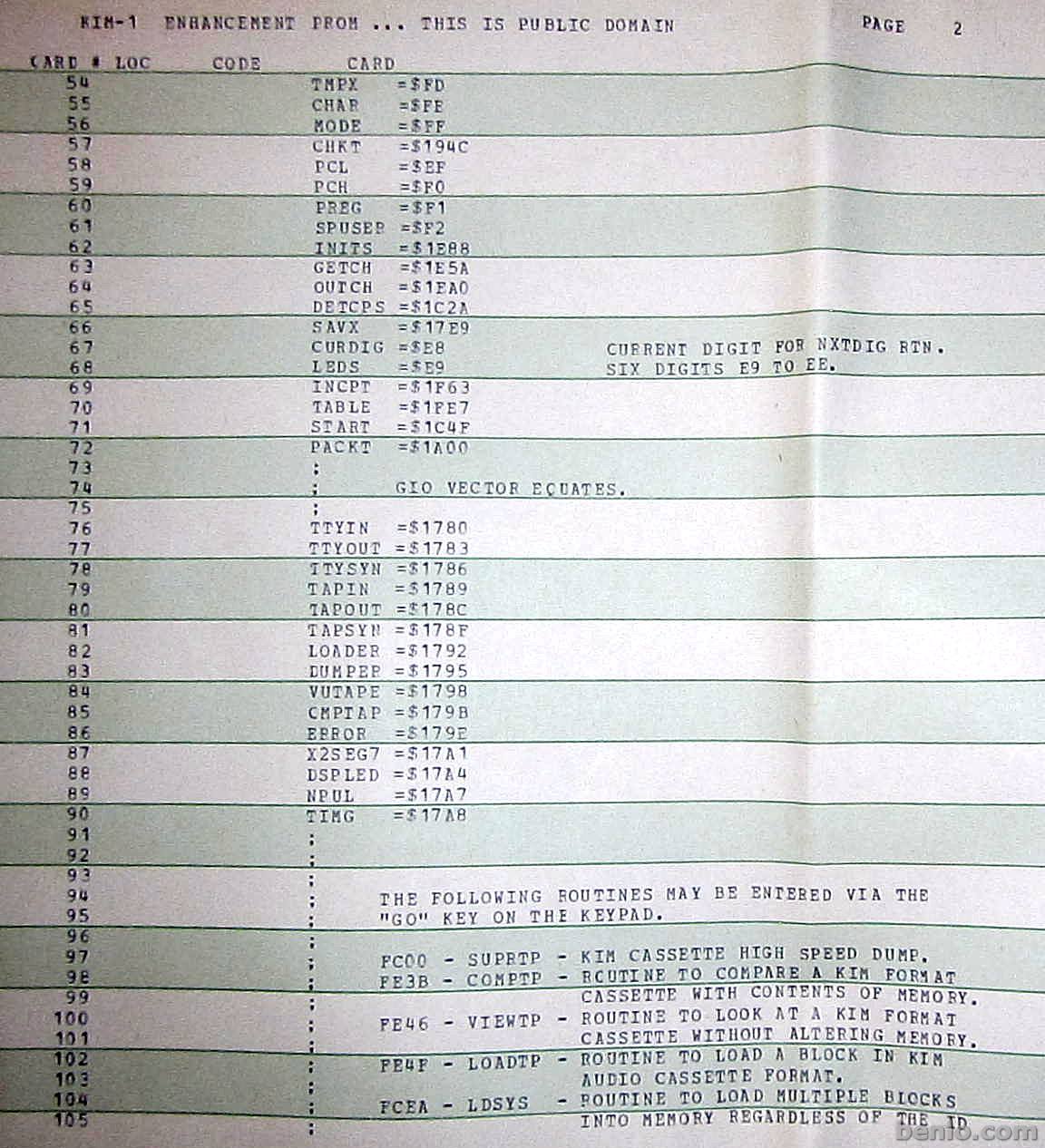
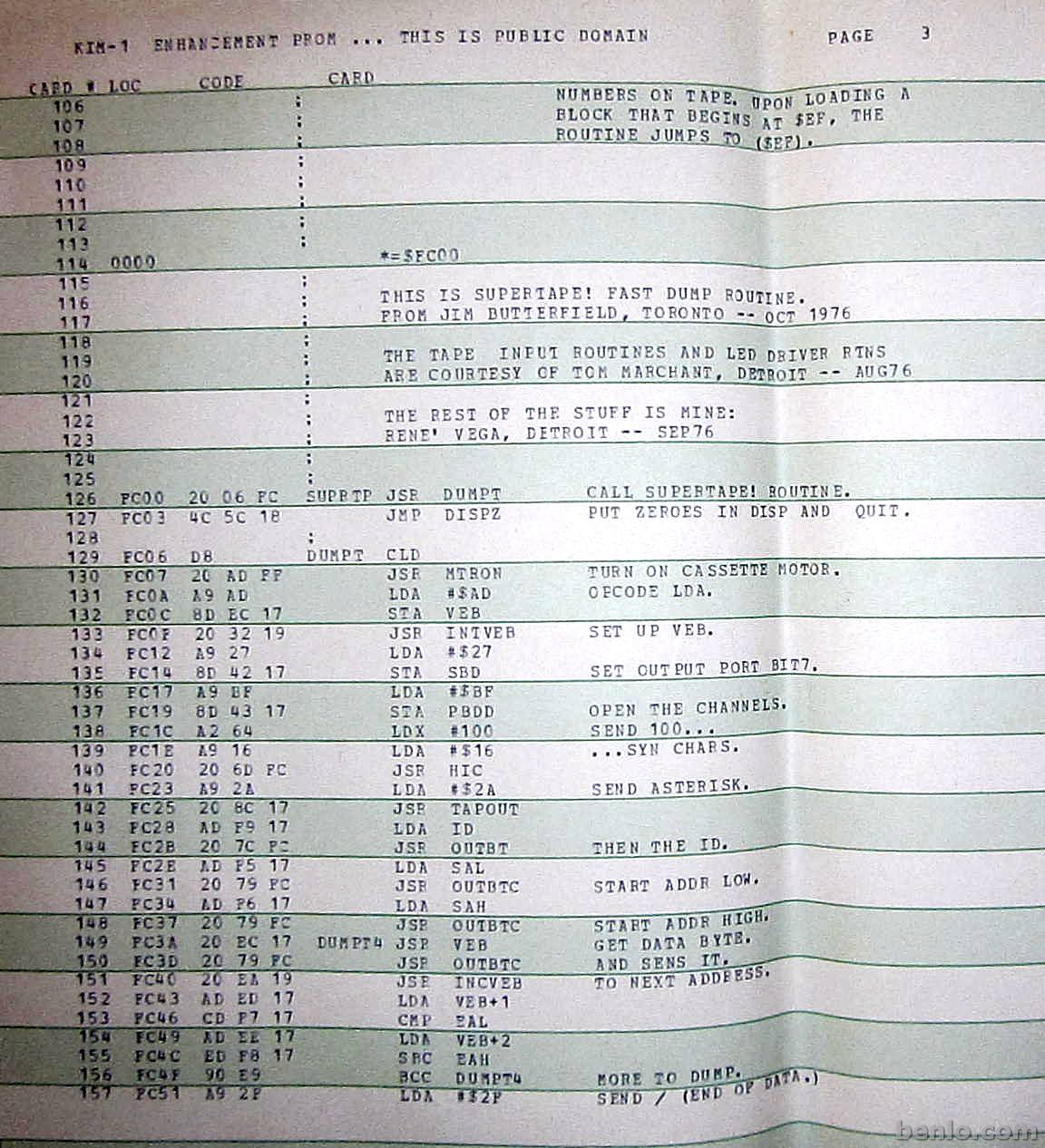
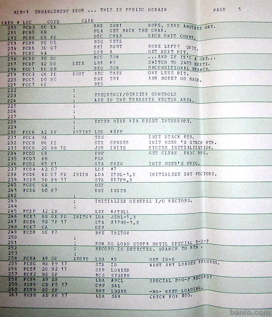
CPM-65, a CP/M-80 analogue operating system for 6502 based microcomputer
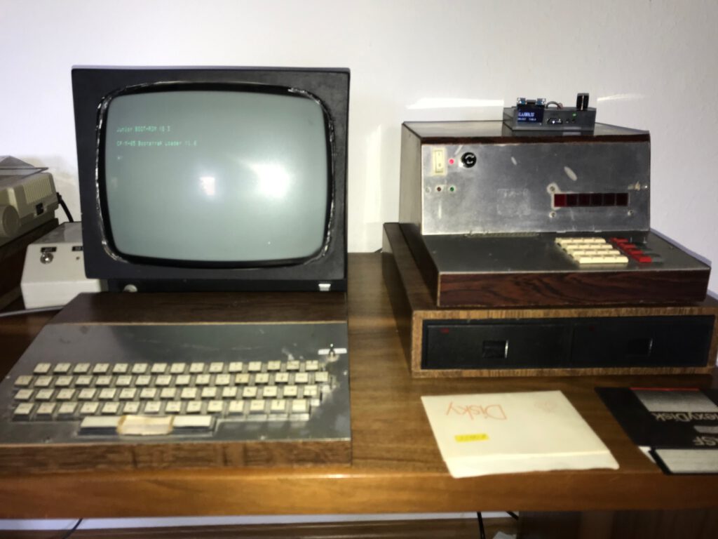
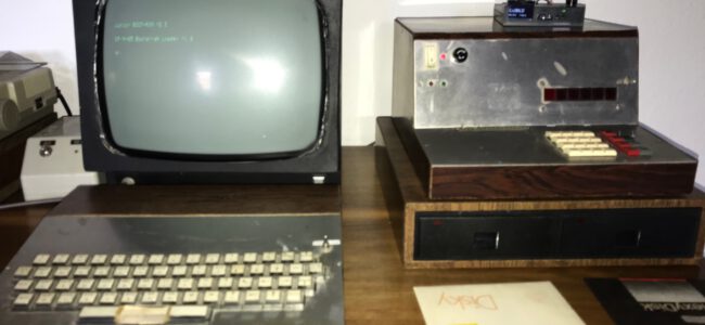
Dietrich Lausberg build a Junior long ago and expanded it to quite a system. He added hardware Elektor components, floppy and hard disk drives and wrote a CP/M inspired operating system, called CP/M-65. He still uses and maintains the system!
All software is published on his github page Dietrich-L
System Requirements
- 6502 processor
- at least 12 kByte RAM
- 6532 I/O chip for the system timer (could be replaced by a 6522 or other)
- minimal 1 Floppy drive
- Serial I/O
The system is a heavily modified and expanded Elektor Junior Computer. For system components and memory map see below.
System Structure
CPM-65 consists of 3 layers:
- BIOS Basic I/O system – currently 3 kB, could be reduced to 2kB by removing SCSI and I2C drivers. Drives can be A-H non consecutive.
- BDOS Basic disc operating system – this is the CPM-65 kernal. Size 2 kB
- CCP Console command program – a simple console which only allows to invoke CPM-65 programs. No resident commands. Size 1 kB
File and Disc Format
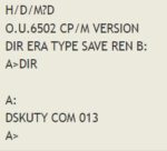
Filenames are CP/M-style d:filename.ext with d
Programs must have .COM as extension and are loaded to $0200 and started there.
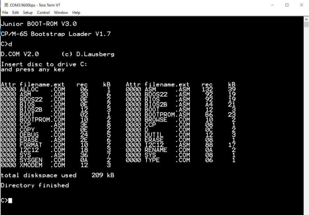
The directory structure is CP/M-compatible and can be read with appropriate tools like CPMTOOLS
The Disc format is typically 40 tracks/ 8 sectors/ 256 byte/sector. It is defined in the BIOS. The BDOS operates on sector numbers. Maximum sector number is $800 blocks with $20 sectors = 65536 sectors á 256 bytes = 16 MBytes
Software List of CPM-65
Name		Version
ALLOC		2.8
ASM	        2.5
BASIC		1.4
BDOS		2.2
BIOS		3.0
BOOT		1.7
BOOTPROM	3.0
BROWSE		1.0
CCP	        1.5
COPY            1.4
D	        2.0
DATETIME	1.1
DEBUG		1.5
DRUCKER		1.0
DUTIL		1.5
EPROMMER	1.2
ERASE		1.5
FORMAT		2.4
FORTH		1.6a
HEXMON		1.1
I2C-UTIL	1.2
RENAME		1.1
RFILE		1.1
SCSIMGR		1.1
STEP		1.0a
SUPERTAP	1.4
SYS 		1.5
SYSGEN		1.0
TYPE		1.6
XMODEM		1.2
Programming
Available software (all written by Dietrich Lausberg)
- Basic interpreter
- Forth interpreter
- Assembler for 6502
All software is supplied as assembler files to be assembled with the CPM-65 assembler.
Hardware
Dietrich Lausberg’s system now has:
- Base Junior
- Interface card
- 64k Universal Memorycard
- 8k RAM/EPROM card
- Universal Disk Controller (Elektor Computing 6) for HD SCSI disk (SD card) and floppy disk
- EPROMmer
- Elekterminal
Modifications made to Elektor cards
- The Junior basecard was mapped to 1K RAM $E000-$E3FF, RIOT at $F600-$F7FF, EPROM was converted to a 2716 and is at $F800-$FFFF
- The Interface card is mapped 1K RAM at $E400-$E7FF, 2K RAM (6116 replacing a 2716) at $E800-$EFFF, the VIA 6522 at $F800-$F9FF.
The tape interface is removed.
- The 64k RAM card from Elektor 83/3-60 (Universelle Speicherkarte) with 48 k RAM (6 x 6264) is mapped to $0000 – $BFFF.
The card has a modification, which allows the Elektor EPROMMER to take over $B000-$BFFF when present on the bus
- The 8K RAM-EPROM card was modified to 4 x 6116 at $C000-$DFFF, 1K RAM $F000-$F3FF
All modifications in the adressing were done with the existing glue logic. I know, its a bit convoluted, but it has evolved over time – actually the last change is from 2021. The system works very stable. So the mapping does not violate the 6502 timing requrements.
The target always was to have as much consecutive RAM from zero page to HIMEM as possible. This is a bit CP/M style and makes it easy for the software to use as much RAM as it can grab until the CCP is met (cwhich is currently at $D800). CPM-65 has up to 53 kB transient memory. The largest program is BASIC, which easily assembles in the RAM to a 10 kB program with 26K to spare. Basic then has 45247 Bytes free.
Drives
- A: and B: 2 x BASF 6108 40 Tracks double density
- C: Gotek with Flashfloppy V3.32 from Keir Fraser emulating another 40 tracks DD drive
- E: and F: SCSI drive SCSI2SD V5.1 by Michael McMaster configured to emulate 2 x 16 MB harddiscs
Serial interface
Serial 1200 – 9600 Baud TTY to ELEKTERMINAL (1200 Baud) or Terminal emulator (600 Baud). As emulator TeraTerm is ued especially for file transfer via Xmodem or a a self-written ELEKTERMINAL emulator. The emulator is necessary, because some of the software, most notably the FORTH screen editor needs the very specific ELEKTERMINAL control codes.
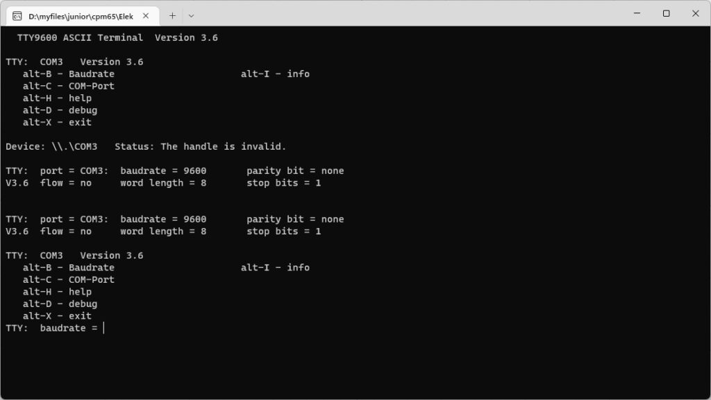
TTY9600 Elekterminal Emulator
This program emulates the ELEKTERMINAL published by the magazine ELEKTOR in November/December 1978.
All software is published on his github page Dietrich-L
The program is written in Free Pascal and compiles in the LAZARUS PASCAL environment. The TTY5.EXE is verified to work under Windows 10 64 bit. No installation is needed, just invoke TTY5
Commands

   alt-B - Baudrate                      alt-I - info
   alt-C - COM-Port
   alt-H - help
   alt-D - debug
   alt-X - exit
Fixed parameters:
	word length = 8
	stop bits = 1
	parity bit = none
	flow = no
These parameters can be changed in the source code only.
ELEKTERMINAL commands
The ELEKTERMINAL uses the SF.F 96364 CRT Controller and some glue logic. The terminal displays 16 lines with 64 characters and interprets some ASCII command codes
Code 	Function
$08	Cursor <--
$09	Cursor -->
$0A	Cursor down
$0B	Cursor up
$0C	Home cursor + clear screen
$0D	Carriage Return
$1A	Clear current line
$1C	Home Cursor
$1D	Cursor to begin of line


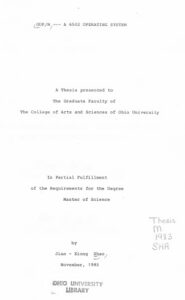
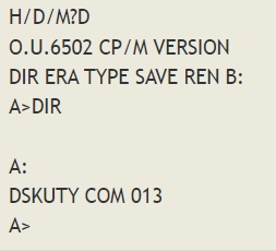 A thesis by Jian – Xiong Shao, 1983, titled OUP/M – A 6502 Operating system, contains a floppy disk based operating system for the 6502. It is modelled after CP/M and follows the same design principles.