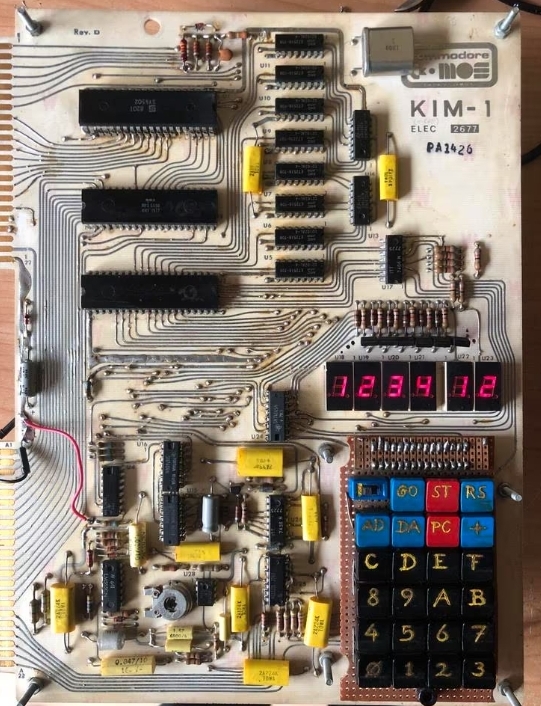
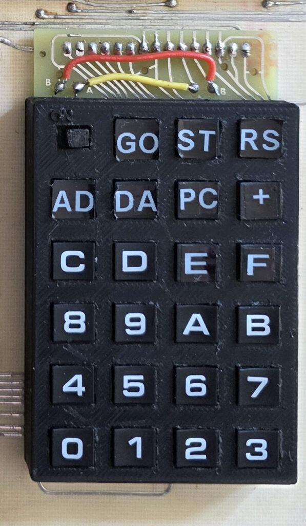
The keypad mounted on a real KIM-1! It fits very well.
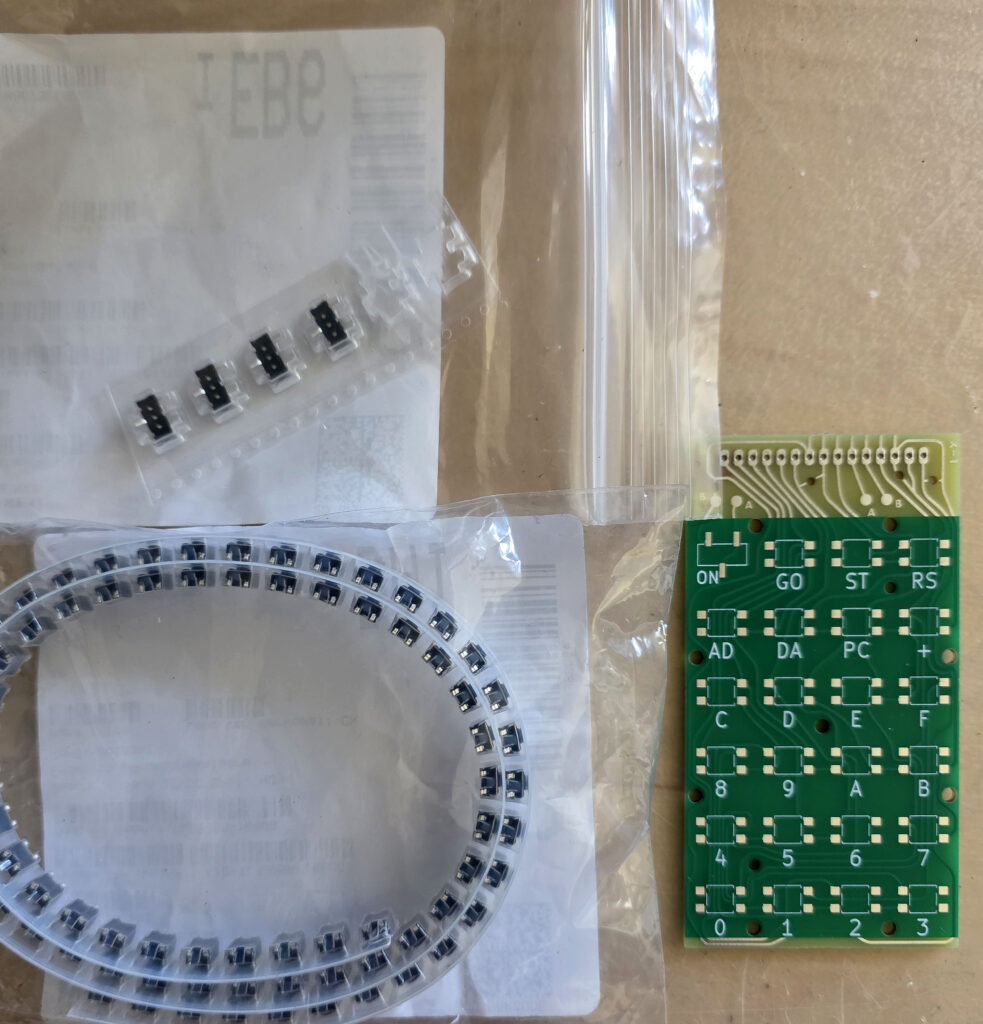
Parts you need
- PCB as designed by Eduardo
- 19 SMD switches TL3305A
- A slide switch JS102011SCQN
- 2 Keypads, as source of keycaps scavenged from keypads sold as AZ-Delivery 4×4 Matrix Keypad, also available cheap on AliExpress.
- 3D STL of frame, either with ON text embossed or without (see below)
- 3D printer, black PLA filament or balck resin, depending on your 3D printer. Or send it off to a 3d printing service. I have used black PLA, my friend Gerben Voort a professional 3D printing service in resin and sanded.
- At least 3 small self tapping screws
- Several self tapping screws to connect the kaypad to the KIM-1 PCB from underneath
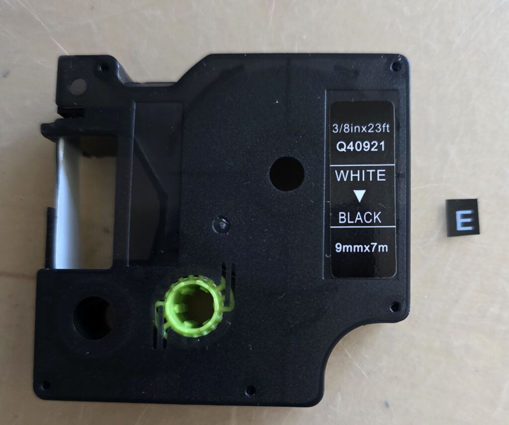
- A label printer like the Dymo Pocket with White on Black tape 9 mm
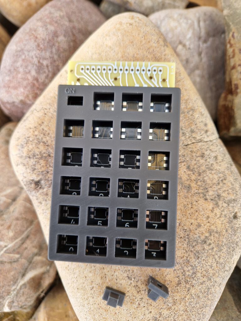
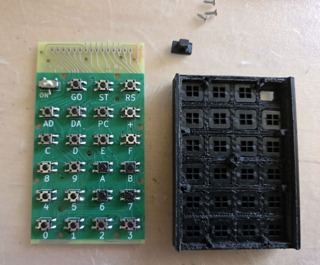
Step 1. Populate the PCB with switches
Get the PCB as designed by Eduardo Casino. The design is available at his github archive. Sent the gerbers to your favorite PCB factory, I use JLCPCB.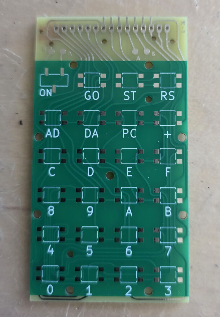
 Surface mount switches and slide switch. Solder one leg first of all switches. Check if the switches are nicely in line with the others. Move if required.
Only when you are satisfied with the position of all switches, solder the other legs. Fine tip, not too much solder.
Surface mount switches and slide switch. Solder one leg first of all switches. Check if the switches are nicely in line with the others. Move if required.
Only when you are satisfied with the position of all switches, solder the other legs. Fine tip, not too much solder.
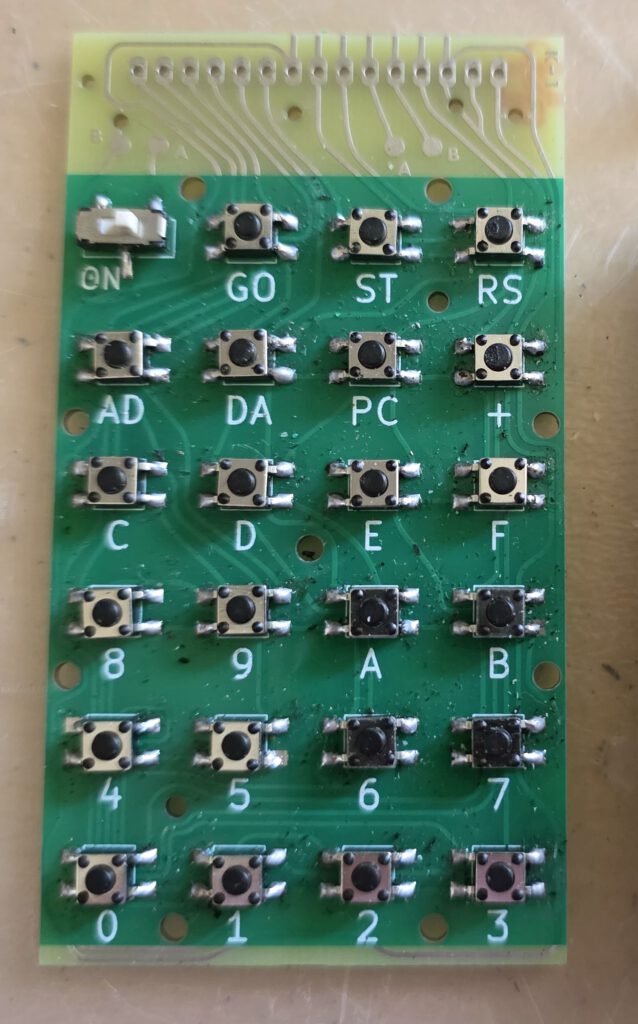 Next solder the two wires (A to A, B to B) on top of the PCB.
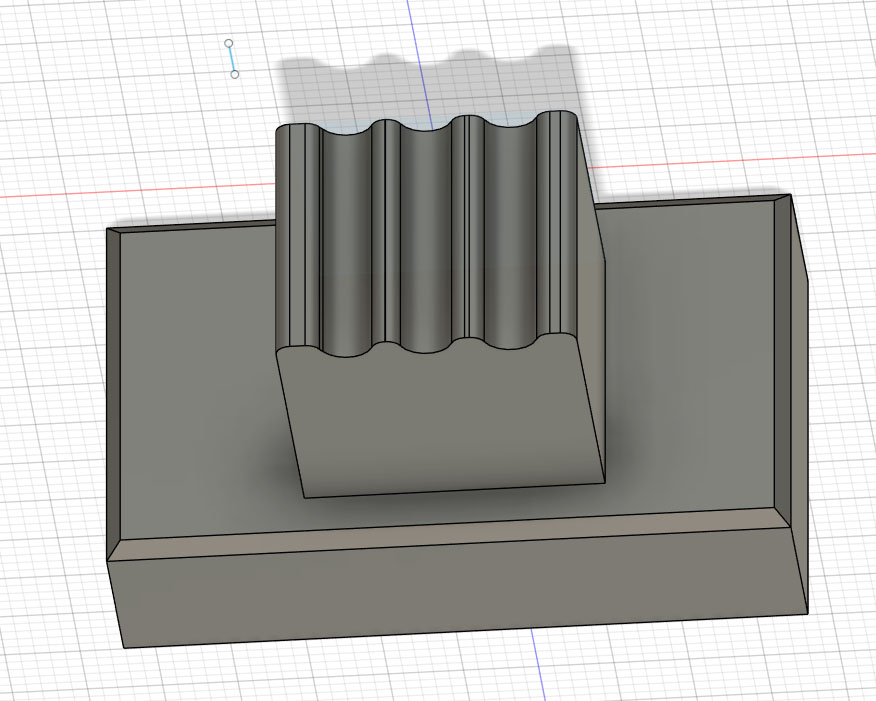
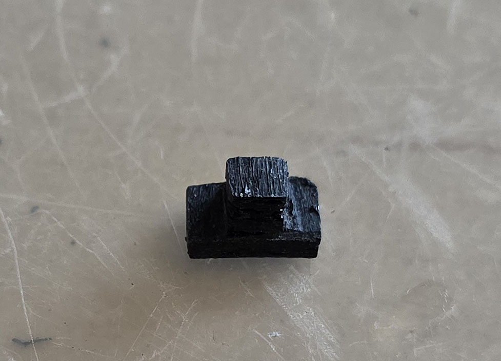
Step 2. Print the frame and the slide switch button
Depending on your printer and wish to be close to the original a choice of two 3D designs has to be made:- The 3D design by Pete (peo2000 on forum64.org) You can print his one with the front on the bottom. No supports required, use fine resolution. That delivered on my 3 printer a quite smooth end result.
- The design enhanced by me with the embossed text ‘ON’ like the original keypad of the KIM. And a small cutout, and ribbles on the SST switch This one needs to be printed with the front of the frame on top due to the embossed text. So it needs supports. This means quite some afterwork to remove the artefacts and the top is not as smooth. The slide switch button is quite small, print in highest quality with a brim.
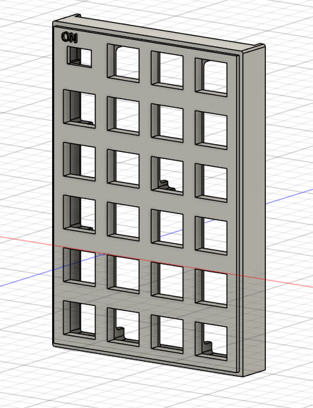
 My friend Gerben Voort uses a 3D printing service. In resin black a near perfect result is achieved.
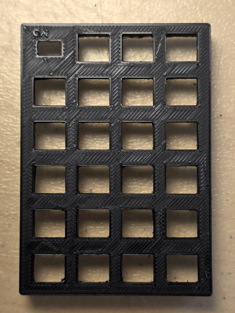
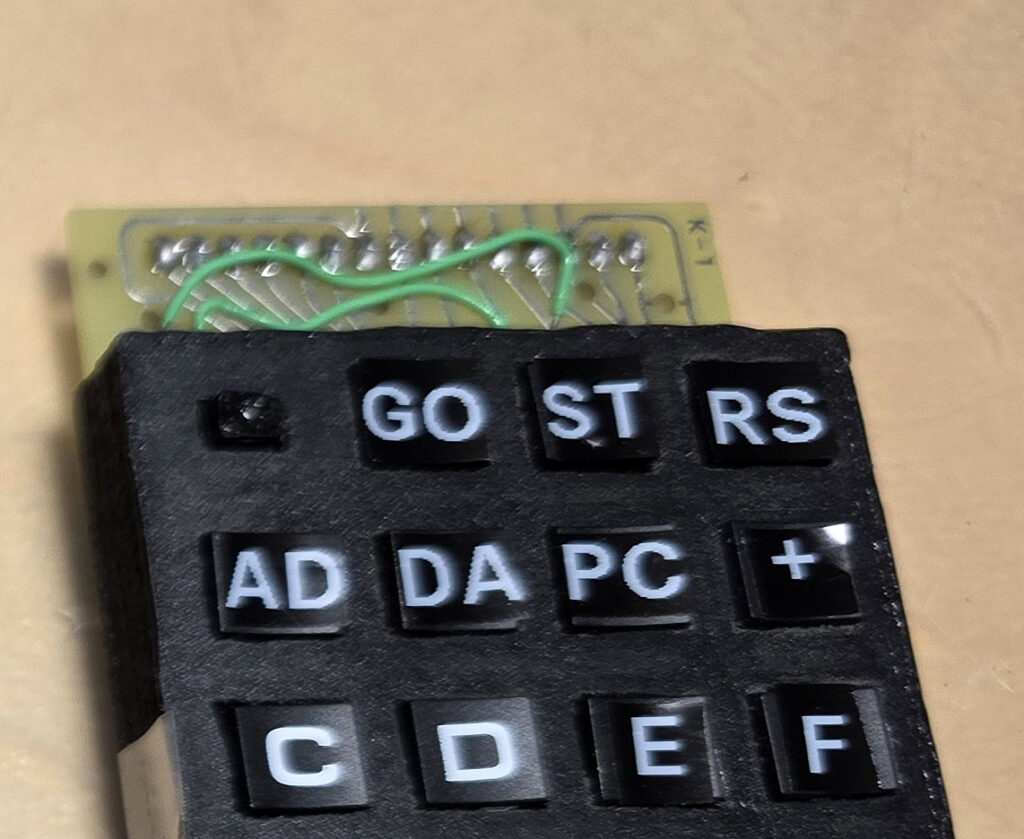
Step 3 Add the keys
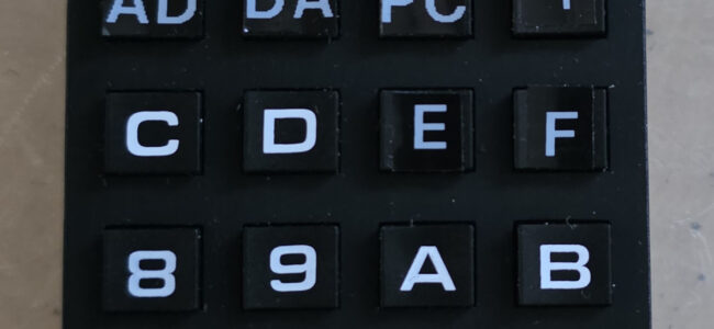
The printed frame is meant to be used with keys scavenged from 4×4 keypads. Break the 4×4 keypad open and take the keys out. As you can see, keys 0,,9 and A..D can be used right away.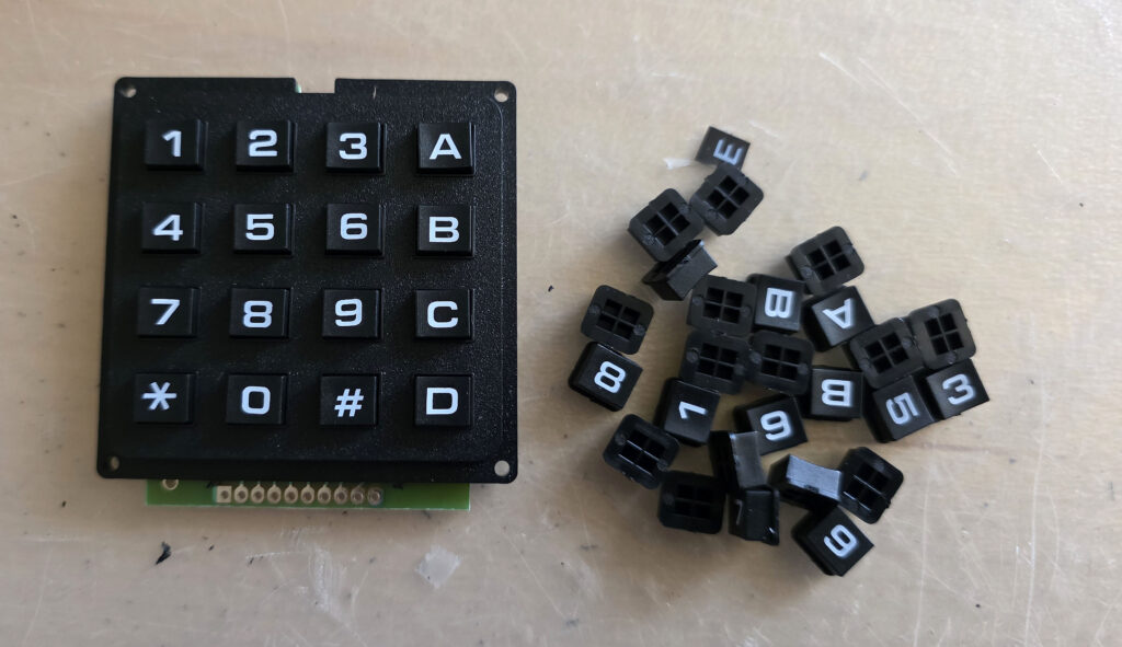 The other keys (E, F, AD, DA, ST, RS, PC, +, GO) need a label. I print those with a cheap Dymo Pocket printer with white on Black 9 mm tape.
The ‘E’ and ‘F’ are printed ‘wide’, the other in normal width.
Cut the label to the right size and put them on the keys.
The other keys (E, F, AD, DA, ST, RS, PC, +, GO) need a label. I print those with a cheap Dymo Pocket printer with white on Black 9 mm tape.
The ‘E’ and ‘F’ are printed ‘wide’, the other in normal width.
Cut the label to the right size and put them on the keys.
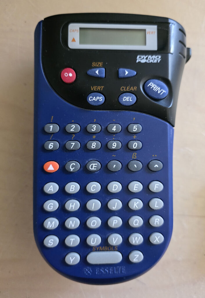 I wish the color white was a bit more white, and the font more like the the other keys, but it is the best I can do with this label printer.
Insert the keys in the frame with the frame top on the table. Put the slide switch button on the slide switch.
I wish the color white was a bit more white, and the font more like the the other keys, but it is the best I can do with this label printer.
Insert the keys in the frame with the frame top on the table. Put the slide switch button on the slide switch.
Step 4 Combine PCB and frame
You now have a PCB with switches and a frame with keys. Put the PCB on the frame and screw some small self tapping screws in the PCB into the frame.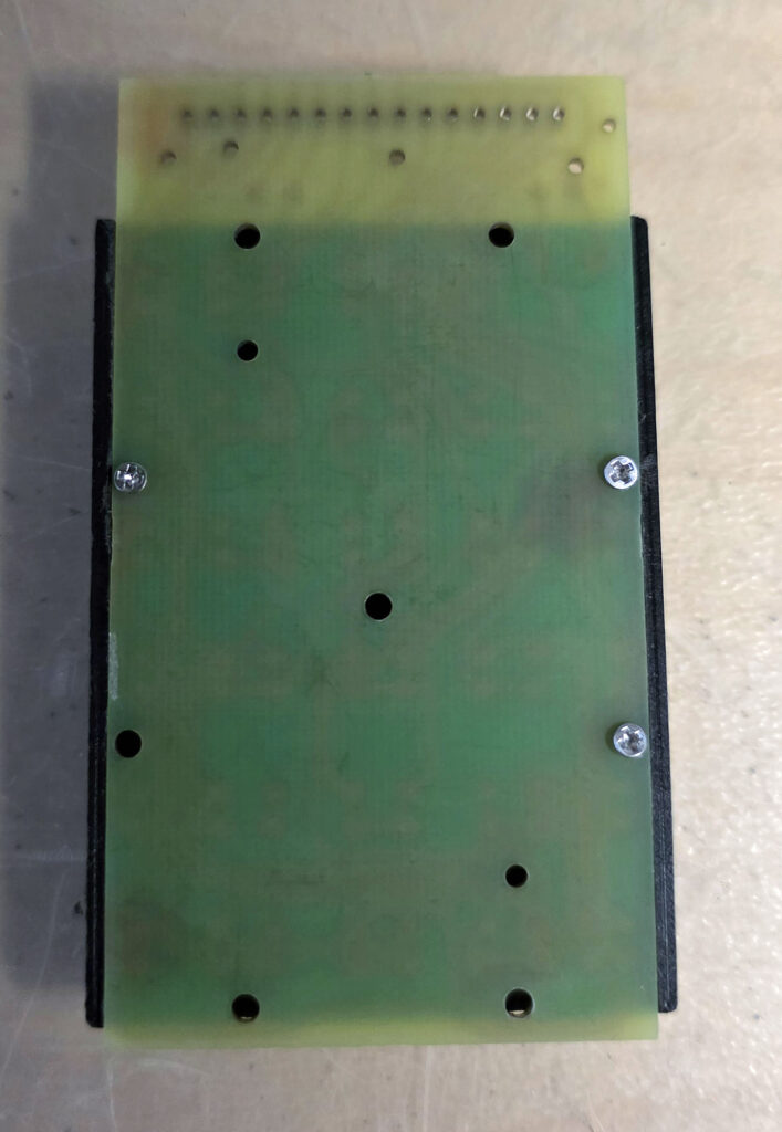
The last step
Check if all keys ‘click’, as in this video.See also:
TERC KIM-1 Interface set
A recent acquisition, the TERC (Technical Education Research Centers) KIM-1 Interface set. An educational tool to work w...
6502 tester NMOS CMOS 1-8MHz
The 6502 W65C02 6502C CPU tester NMOS / CMOS 1-8MHz is a CPU tester for 40 pin 6502/65C02 and WD65C02 and Sally.
The...
680x/650x Test system
The 680x/650x Test system allows to test, with the CPU itself performing the test, the MC680X and MCS650X families.
T...
Backbit Chip Tester PRO V2
A simple tio use and effective component test and ROM dump can be done with the wonderful Backbit Chiptester Pro V2.
...