
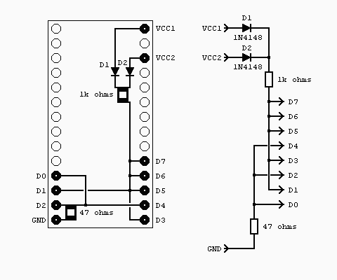
6502 NOP generator circuit.
Here’s a simple circuit, built from bits in the junk box, that has saved many hours of head scratching when that just finished new 6502 circuit failed to work first time.
What does it do? Well nothing much, in fact a lot of nothing much’s as it pulls the data lines on a 6502 to the NOP ($EA) opcode.
The circuit is built on a small piece of stripboard that has been soldered onto a 28 pin turned pin I.C. socket. This is the only important part of the project, use decent (i.e. stiff and thin) pins. Don’t be tempted to use IDC header type pins, as they are too thick and will ruin the socket you push them into. If you have them use I.C. header pins, I didn’t but a turned pin socket, used as a header, is just as good.
The two diodes, I used 1N4148s but any small signal or shottky diode will do, are to allow the use of this generator in either 24 or 28 pin sockets. If you are only ever going to use one type then the diodes can be omitted and the 1k resistor tied directly to the +5v pin.
The 1k resistor is used to pull up the five data lines that need to be at logic 1, I could have used five 4k7 resistors but I’m lazy. This works just as well.
The 47R resistor in the pull down path is just there to limit any possible ground path fault current to around 100mA, while still providing a firm logic 0 to the data bus. Any value from 33 to 100 ohms should do just as well.
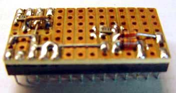
The finished board.
Using it
So your latest 6502 whizzymajig is DOA. Even a short test program doesn’t seem to work. So how will this help?
Replacing the system ROM with the NOP board, and with the help of a logic probe, allows you to verify that you at least got all the data lines connected and in the right order. While you’re there you can also check the data lines to the RAM, I/O and any other chips that connect to the data bus.
So the data lines are all connected ok, now on to dynamic testing. With just the CPU and the NOP gen the CPU should do a read cycle at all 65536 addresses in sequence. If you have a scope with at least an external trigger, or better yet with two channels, you can trigger from some known signal and see if other signals are behaving as expected.
Example signals
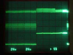
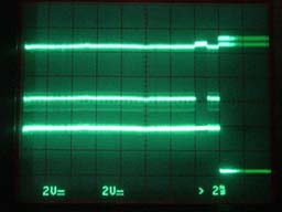
For example, if you trigger off the falling edge of A15 and set your scope to display the whole A15 low/high cycle in eight divisions of your scope screen then each division becomes 8k wide. From this you can easily see if chip select and other decode signals are at least in the right part of the address range.
If you trigger of an edge of A15 and set your scope to display the low, or high, half of the cycle in eight divisions then each division becomes 4k. With this you can easily see the 2k block of memory that is NOT decoded for the ROM because that is where the I/O lives.
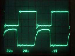
You can also trigger off faster signals, such as phase 02, and check individual access cycles to particular devices.
Even if you don’t have a scope you can still do some basic dynamic tests. Using a piezzo sounder connect between A15 and ground, you should (just) hear a low pitch buzz. This will be about 15Hz on a 1MHz 6502 and 30Hz on a 2MHz 6502. You can then step through each line in turn and the pitch should double each time. Once the pitch gets too high to hear you can use a lower clock to check the lower address lines. You can also check the connection of other devices to the address bus by connecting one wire from the sounder to an address line on the CPU and the other wire to the corresponding address on the ROM, RAM or I/O chip. If all is well you should hear nothing, if there is a wrong connection you should hear a tone.
If you need to test write cycle decoding then lift the R/W pin on the CPU and tie the R/W line to 0v. The processor will still do read cycles but the decode logic will see them as write cycles.
There are probably many ways to improve this circuit but it was built from scrap, to do one thing, in about twenty minutes. I’ve found it very useful, I hope you do too.