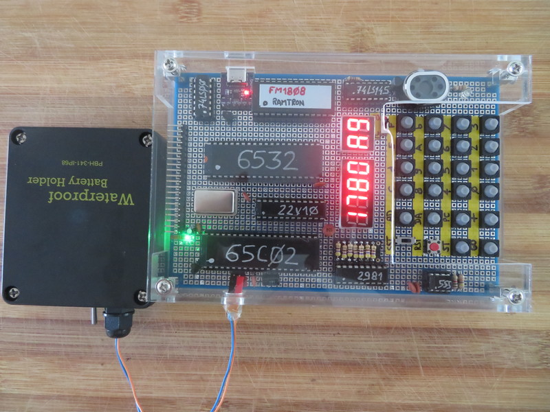
Small enough to take with you traveling, battery powered and thanks to the FRAM the contents of RAM are kept when powered off.
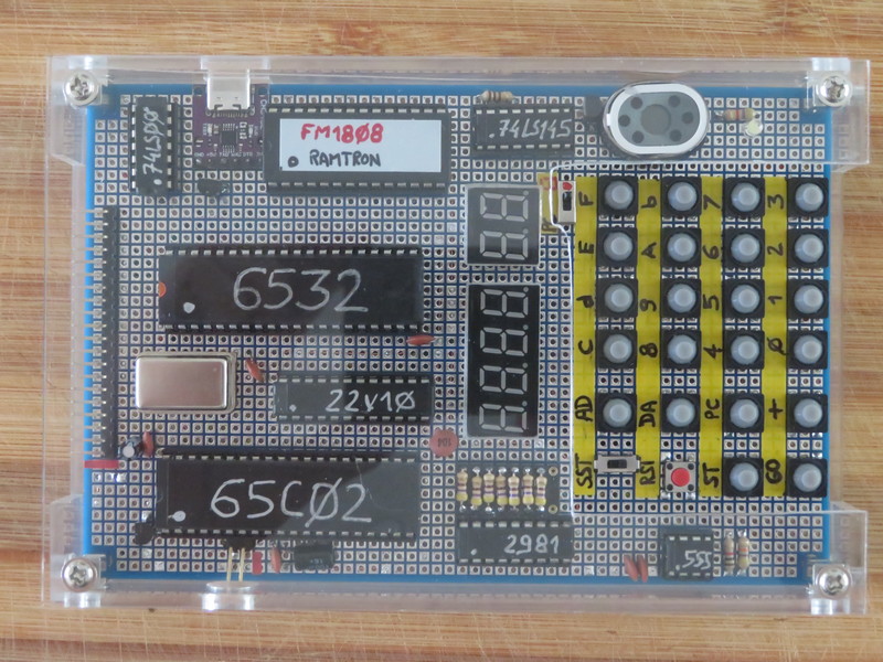
The FM1808 used is a non-volatile RAM (32Kx8), used here for ROM and RAM. Datasheet here.
This design appeared in the Google group devoted to the PAL-1 and PAL-1 (and the KIM-1 of course).
The design is by Voyageur.
And this is how Voyageur describes it:
A modified replica, created for travel and easy to use. The acrylic case is supposed to protect the plate.
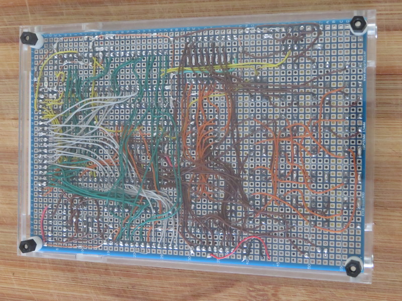
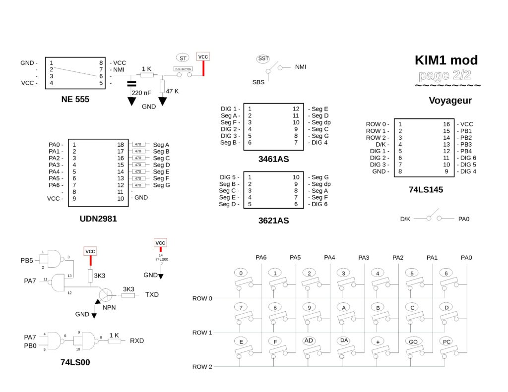
Board format 10 x 15 cm, 32 KB of RAM and/or ROM, an expansion connector for daughter-boards, a speaker and a white LED for debugging purpose.
Some other explanations :
The original casing comes from a ‘Schumann wave generator’ sold on eBay as is.
I therefore decided to use this casing for my KIM1 travel project. It had to be cut down a bit to allow access to the keyboard.
- my version of the Memory Map (see below) or here ‘MemoryMap.txt’
- the GAL manages all addresses between RAM, ROM and I/O (from $0000 to $FFFF).
See here the ‘KIM1mod.pld’
and it’s easy to change the addresses with WinCUPL and to adapt to any need… - the FRAM RAMTRON FM1808 can keep out of power all the contents of the ROM and the RAM
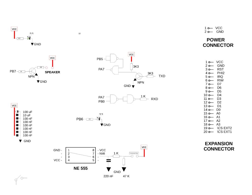
(here is a 32 KB capacity). - the speaker is linked to PB7 of the RIOT 6532 (which is not used for Tape).
- the white LED is linked to PB6 of the RIOT 6532.
- the Monitor location (ROM as specified in KIM1mod.pld) has the KIM-1 6530-002 (I don’t plan to use the TAPE storage) and the WozMon.
- the small USB TTL is a CH340E module, non expensive and easy to find a place on a board. I use a USB C retractable cable.
- the portable power supply is fit with a 5V Step-Up/Step-Down small module from Pololu and can accept four rechargeable or Alkaline batteries.
- the KIM-1 MOD current used is less than 175 mA
- the NE555 has the same function as half the 556 in the KIM-1 circuit diagram (about the \NMI STOP switch).
- the 20 pin expansion connector accepts any daughter-board equipped with 65(C)22, 6821, 82C55, 6850, or ….
- the RESET circuit is a DS1813-10.
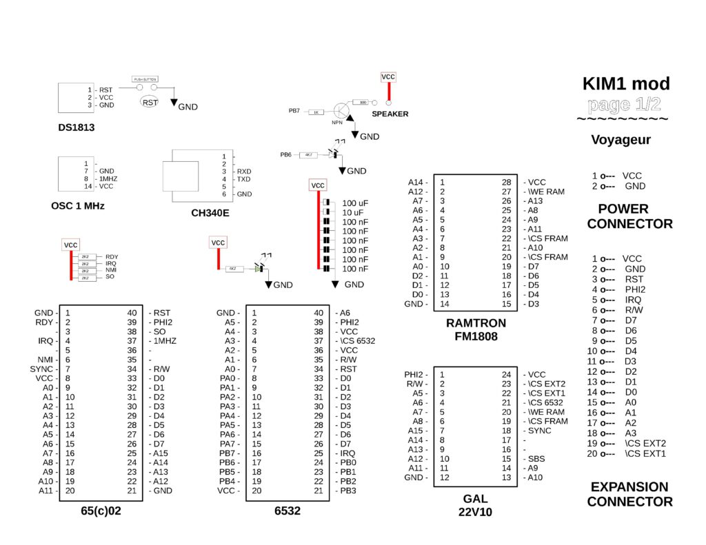
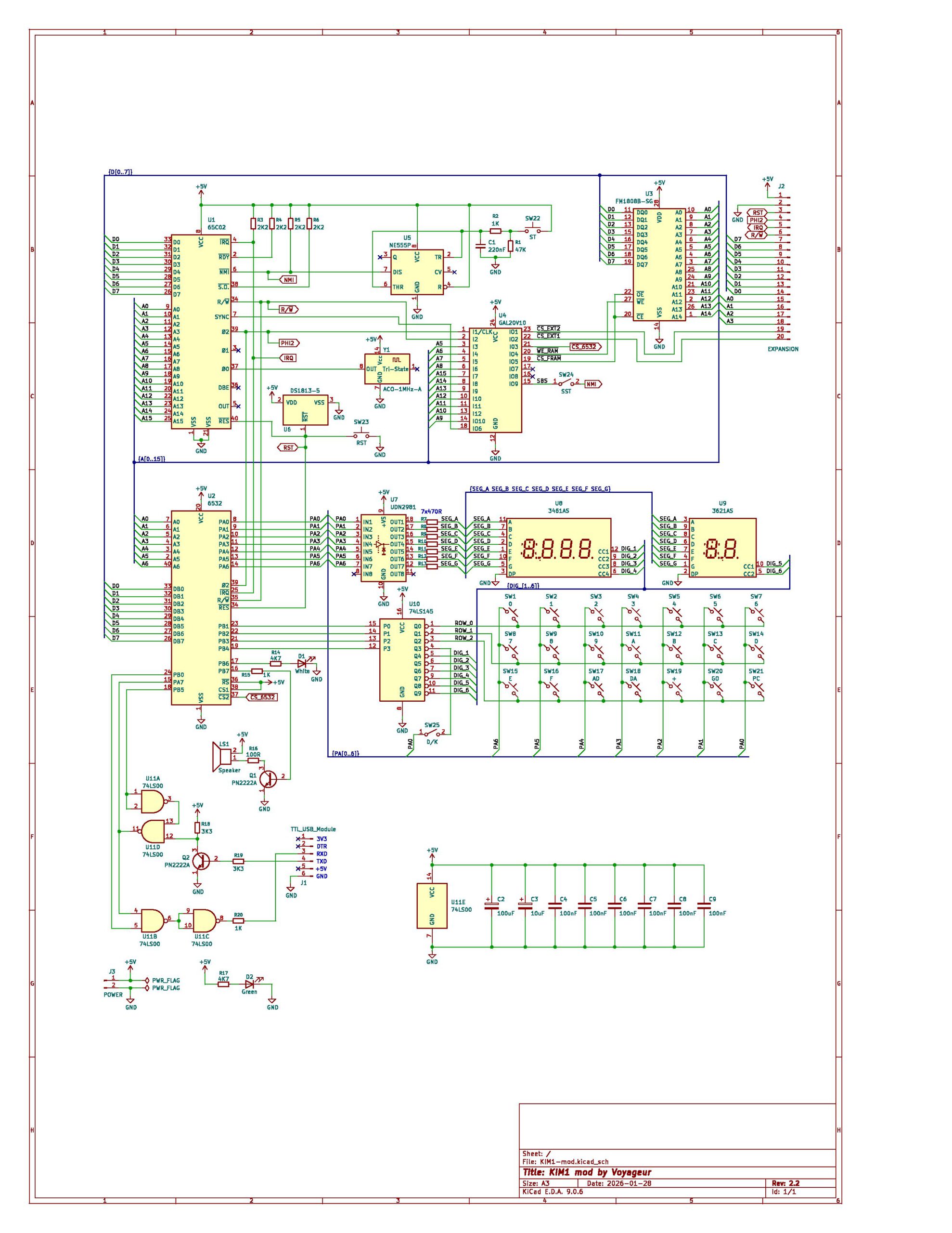
Circuit diagram entered in Kicad, by Eduardo Casino, untested!
  ---------------------------------------------
  |                MEMORY MAP                 |
  |				              |
  |  $E000...$FFFF       ROM User        8 K  |
  |                      and 6502 vectors     |
  |                                           |
  |  $6000...$DFFF       not used       32 K  |
  |                                           |
  |  $2000...$5FFF       RAM3           16 K  |
  |                                           |
  |  $1800...$1FFF       ROM Monitor     2 K  |
  |                                           |
  |  $1780...$17FF       RAM2          128 B  |
  |                                           |
  |  $1740...$177F       \CS RIOT       64 B  |
  |  $1720...$173F       \CS EXT2       32 B  |
  |  $1700...$171F       \CS EXT1       32 B  |
  |                                           |
  |  $0000...$16FF       RAM           < 6 K  |
  |                                           |
  ---------------------------------------------
Software
The ROM part of the KIM-1 MOD in the FM1808 consist of the KIM ROM (in the 6530-002), and Wozmon adapted for the KIM-1, placed at the empty space of the 6530-003 audio tape routines.
You find Wozmon at $1AA0 and the KIM monitor at $1C00.
Also the 6502 vectors at $FFFC-$FFFF are set to the KIM-1 -002 ROM.
There is enough space in $E000-$FFFB for other software.
To write to the FM1808, use the TL 866-II Plus or the XGecu T48.
Attached the complete dumb of the FM1808 in binary.
Download here 32K contents of the FM1008
The KIM ROM has a small modification
 747                  ;       ** INITIALIZATION FOR SIGMA **
 748  1E88  A2 01     INITS   LDX   #$01      SET KB MODE TO ADDR           1E88
 749  1E8A  86 FF             STX   MODE
 750  1E8C  A2 00     INIT1   LDX   #$00
 751  1E8E  8E 41 17          STX   PADD      FOR SIGMA USE SADD
 752  1E91  A2 FF             LDX   #$FF      was #$3F PB0..PB5 output, PB6 & PB7 input
 753  1E93  8E 43 17          STX   PBDD      FOR SIGMA USE SBDD now PB0..PB7 output
 754  1E96  A2 07             LDX   #$07      ENABLE DATA IN
 755  1E98  8E 42 17          STX   SBD       OUTPUT
 756  1E9B  D8                CLD
 757  1E9C  78                SEI
 758  1E9D  60                RTS
to manage the outputs to speaker (PB7) and the white Led (PB6).
The white Led is off during normal use of the board, except for RESET or High level to PB6
PLD file
Download here the ‘KIM1mod.pld’
Name     KIM1mod ;
PartNo   00 ;
Date     22/01/2026 ;
Revision 01 ;
Designer Engineer Voyageur;
Company  dC ;
Assembly None ;
Location Australia ;
Device   g22v10 ;


/*  for NEW SBC KIM_1_mod                 */
/*                                        */
/*                      compiles   OK     */
/*                      works      OK     */


/* *************** INPUT PINS *********************/
PIN 1   =  PHI2                   ; /*                                 */
PIN 2   =  ERW                    ; /*                                 */
PIN 3   =  A5                     ; /*                                 */
PIN 4   =  A6                     ; /*                                 */
PIN 5   =  A7                     ; /*                                 */
PIN 6   =  A8                     ; /*                                 */
PIN 7   =  A15                    ; /*                                 */
PIN 8   =  A14                    ; /*                                 */
PIN 9   =  A13                    ; /*                                 */
PIN 10  =  A12                    ; /*                                 */
PIN 11  =  A11                    ; /*                                 */
PIN 13  =  A10                    ; /*                                 */
PIN 14  =  A9                     ; /*                                 */
PIN 18  =  SYNC                   ; /*                                 */

/* *************** OUTPUT PINS *********************/
PIN 15  = !SBS                    ; /*                                 */
PIN 19  = !CSROAM                 ; /*                                 */
PIN 20  = !WERAM                  ; /*                                 */
PIN 21  = !CS6532                 ; /*    $1740 - $177F      64 B      */
PIN 22  = !CSEXT1                 ; /*    $1700 - $171F      32 B      */
PIN 23  = !CSEXT2                 ; /*    $1720 - $173F      32 B      */

/*  DECLARATIONS AND INTERMEDIATE VARIABLES DEFS  */

field ioaddr = [A15..5] ;
RAM_eqn = (ioaddr:[0000..16FF]) ;
EXT1_eqn = (ioaddr:[1700..171F]) ;
EXT2_eqn = (ioaddr:[1720..173F]) ;
RIOT_eqn = (ioaddr:[1740..177F]) ;
RAM2_eqn = (ioaddr:[1780..17FF]) ;
ROM_eqn = (ioaddr:[1800..1FFF]) ;
RAM3_eqn = (ioaddr:[2000..5FFF]) ;
ROM2_eqn = (ioaddr:[E000..FFFF]) ;

ROAM_eqn = RAM_eqn # RAM2_eqn # RAM3_eqn # ROM_eqn # ROM2_eqn ;
TOTRAM_eqn = RAM_eqn # RAM2_eqn # RAM3_eqn ;
SBS_eqn = TOTRAM_eqn & SYNC ;


/*   LOGIC EQUATIONS   */

CSROAM = ROAM_eqn & PHI2 ;
WERAM = TOTRAM_eqn & (!ERW & PHI2 ) ;
CS6532 = RIOT_eqn ;
CSEXT1 = EXT1_eqn ;
CSEXT2 = EXT2_eqn ;
SBS = SBS_eqn ;