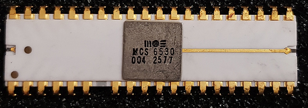
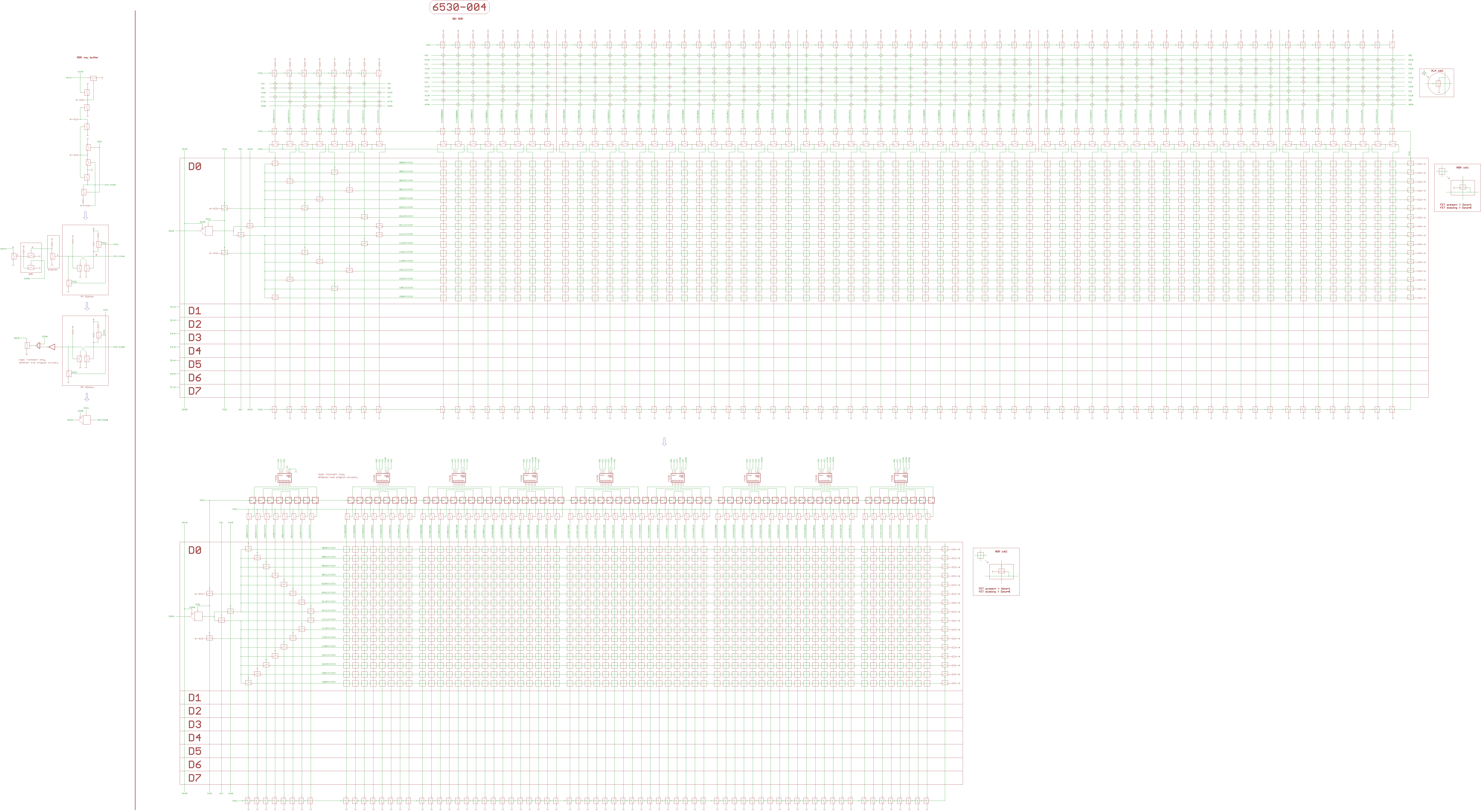
This page about the 6530-004 dissection is about a transistor level dissection of the 6530-004 (TIM edition), brought to you by Frank Wolf and Dieter a.k.a. ttlworks. Published, as before at the 6502.org forum, with permission by Frank Wolf and ttlworks.
Contents
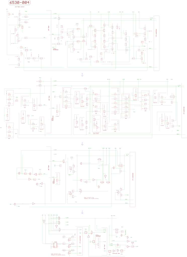
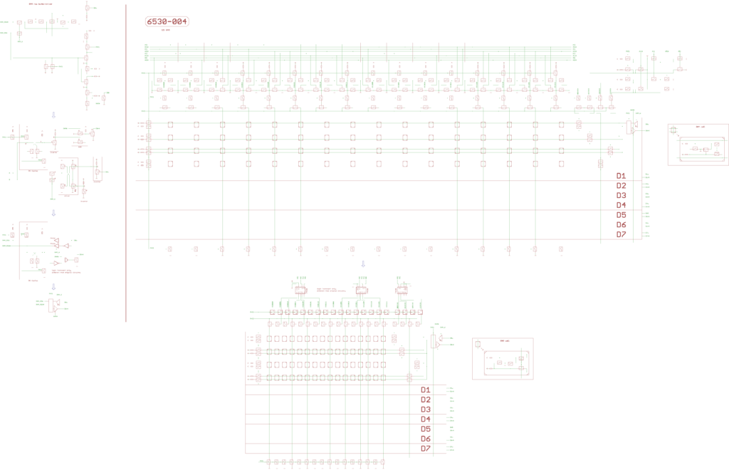
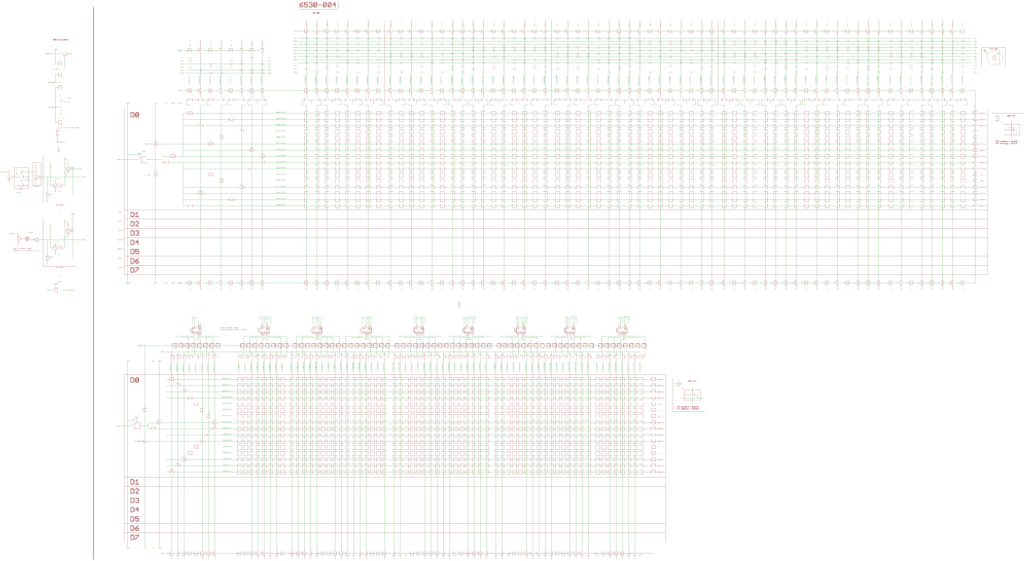
EagleCAD schenatics archive download
Imported in Kicad, exported as SVG images on this page:
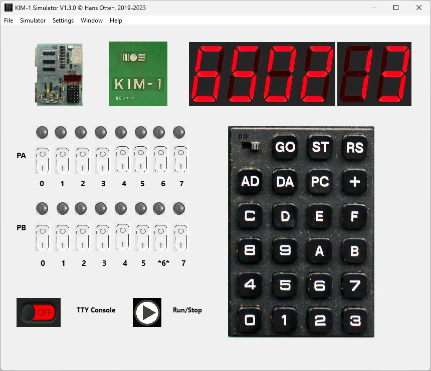
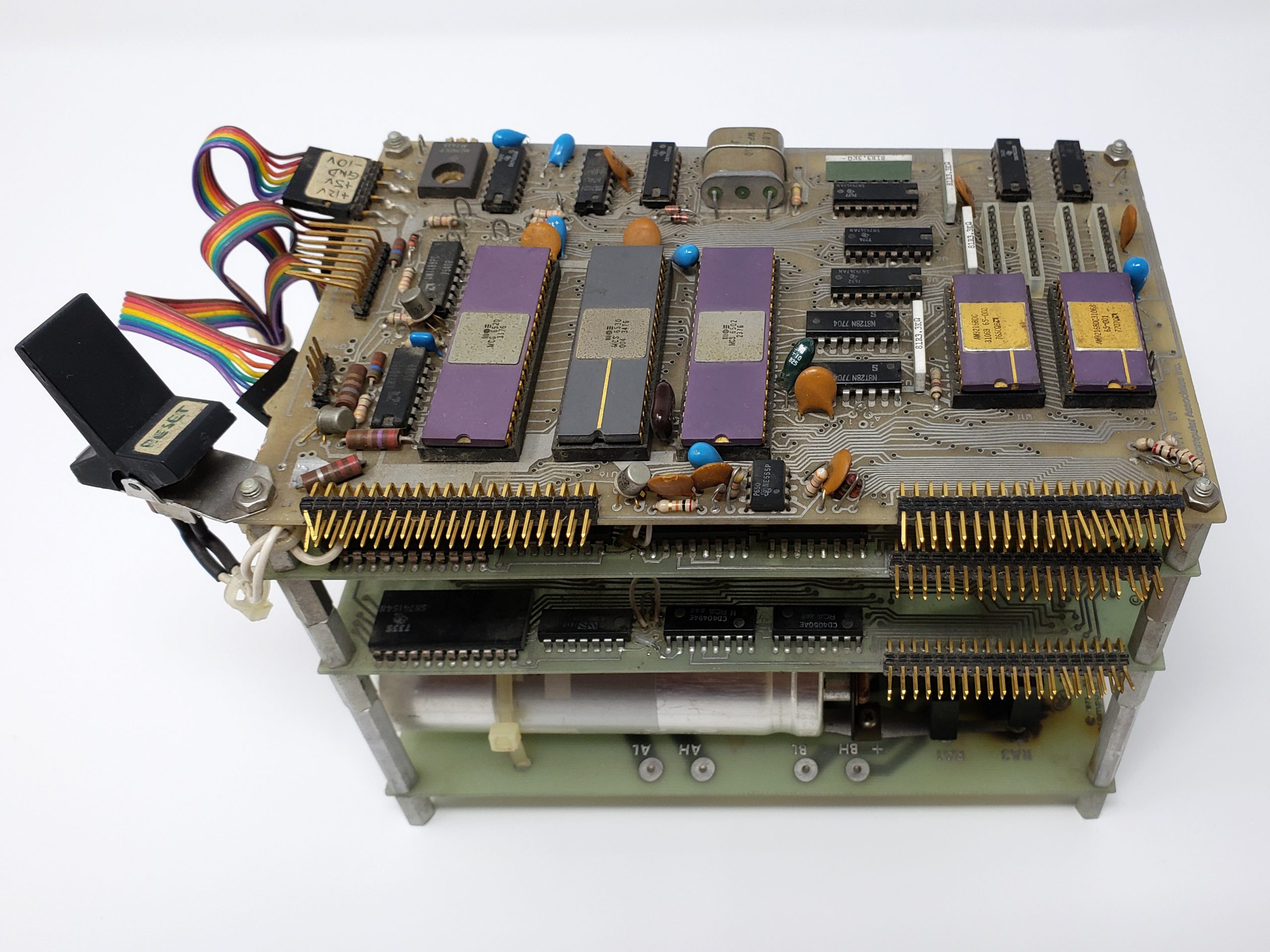
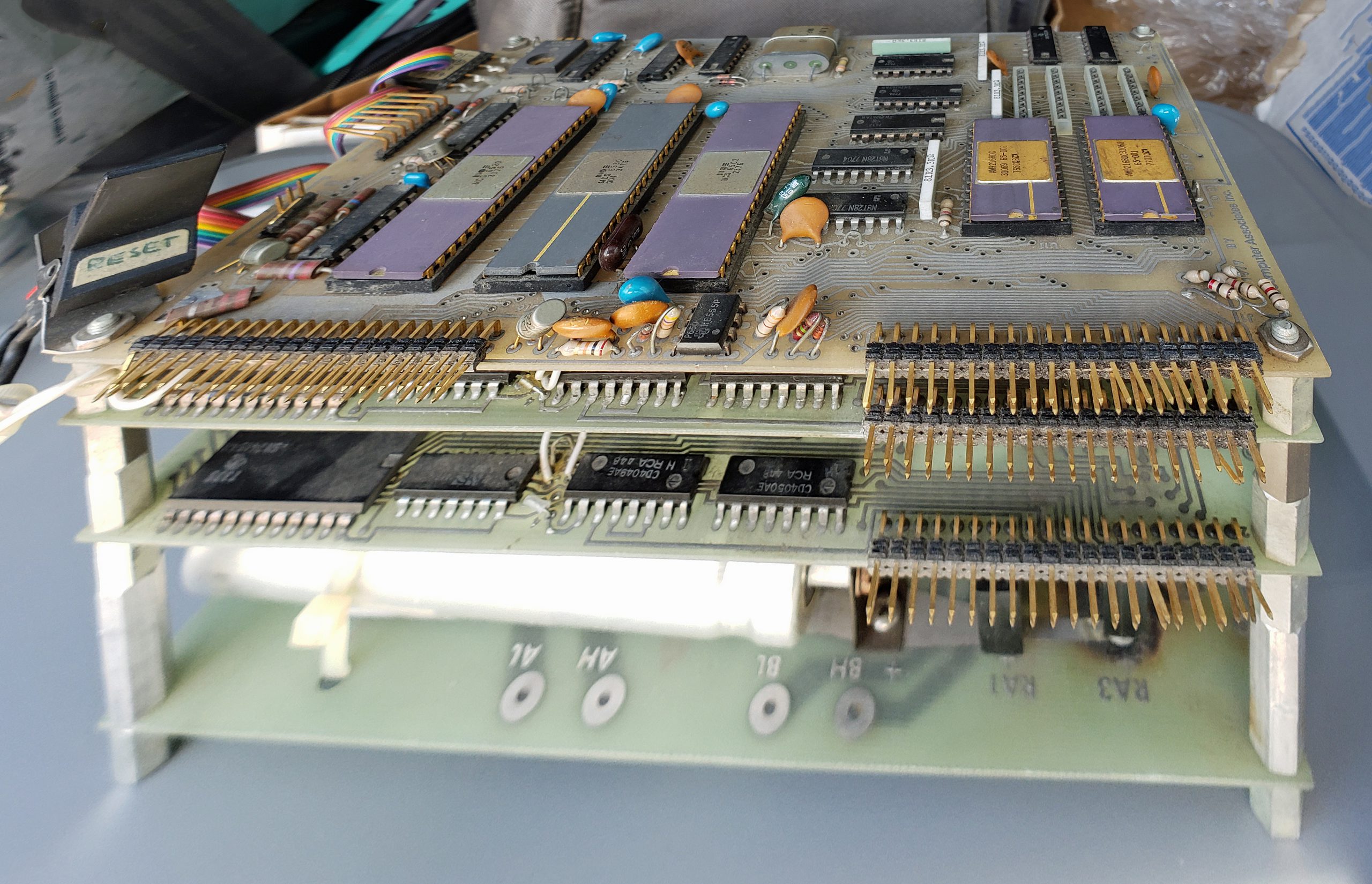
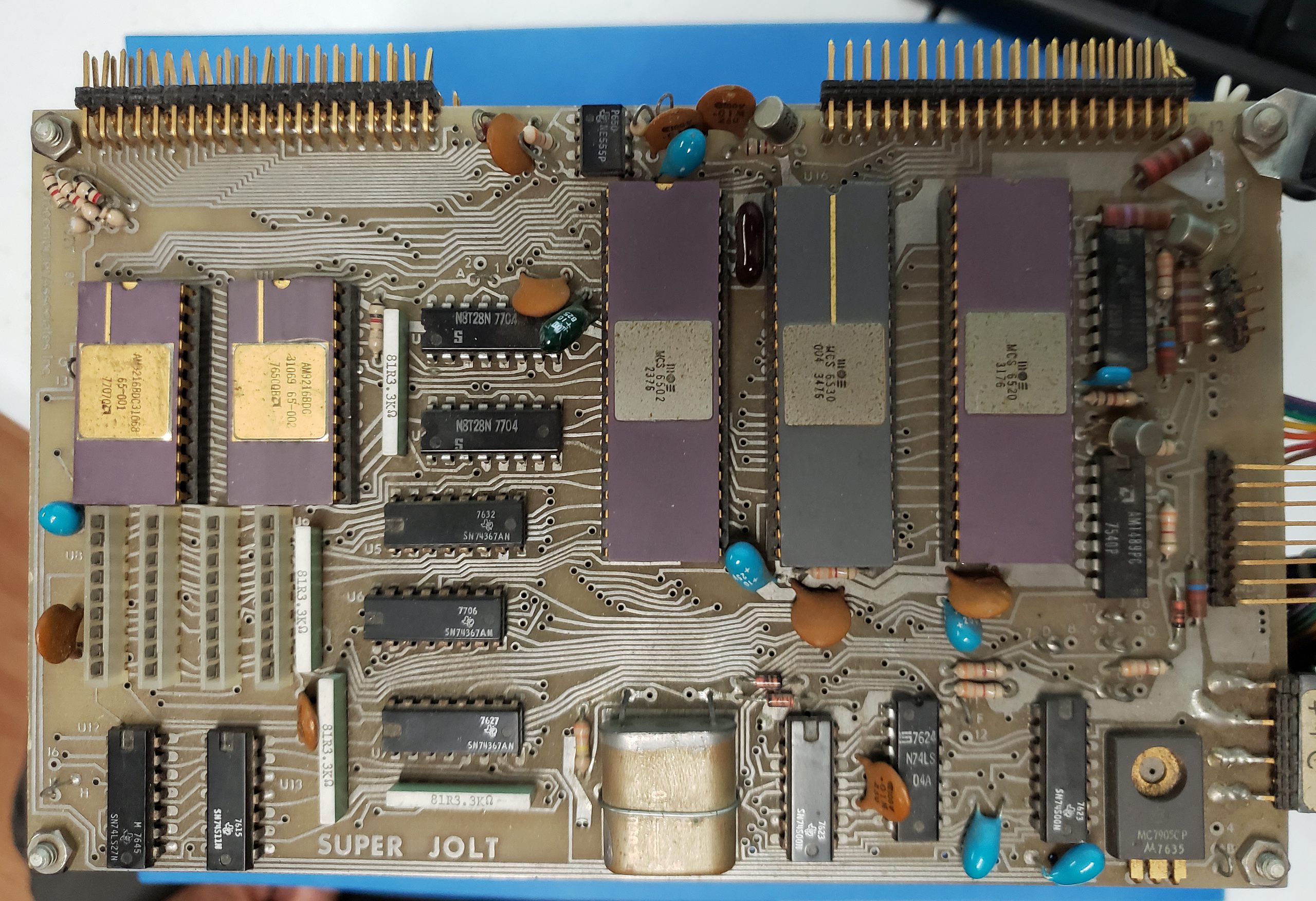
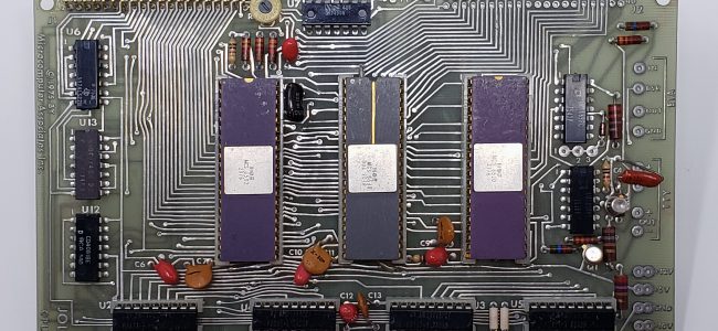
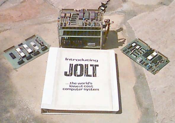
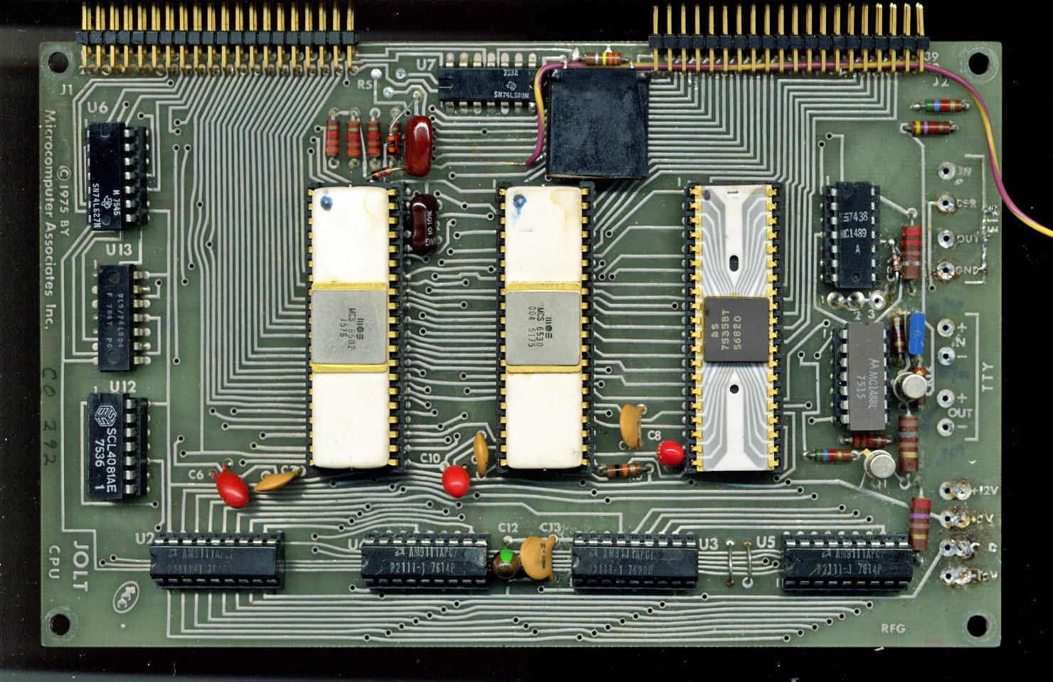
The 6530 was used in the KIM-1, in Commodore disk drives, and in pinball machines.
The 6530 RRIOT (RAM, ROM, IO, Timer) is a special chip in the 6502 family.
6530 contains 64 Bytes of RAM, 1kB of mask programmed ROM, two 8 Bit IO ports, and a Timer.
//Timer is an 8 Bit down counter with pre-scaler factors 1, 8, 64, 1024.
It also contains a mask programmed address decoder.
The idea at MOS Technology was, that a microcontroller could be built from just two chips: 6502 plus 6530.
And that up to seven 6530 (each chip containing a different address decoder and different ROM contents)
could be used in a 6502 system.
And that’s where trouble starts:
Because of custom address decoder and custom ROM contents, when replacing a defective 6530, you can’t just buy any 6530, plug it into the socket and hope that it works. Even replacing a 6530 with a 6530 pulled from another socket from the same PCB probably won’t work.
It has to be a 6530 which fits to a specific socket on a specific PCB, and you need to look out for obscure chip markings and part numbers.

6532 seems to be based on the 6530, it lacks the address decoder and the ROM, but it has 128 Bytes of RAM.
6532 was used in the Elektor Junior computer and in the Atari 2600.
6530 contains some circuitry you probably won’t expect to see in other 65xx peripheral chips (except for 6531 and 6532).
When I was a kid, I did two layer PCB layouts on transparent foil with tape and rub-on dry transfers,
and I think I know how the game goes when things are starting to get a bit dense and complex.
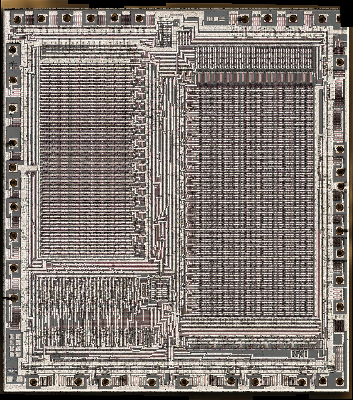
The 6530 chip layout has that “hand routing smell” all over, it’s incredibly dense/compact and complex,
and I feel a need to salute to the designers (Bill Mensch et al.): it truly is a beautiful/amazing work of art.
Again: my thanks to Frank Wolf, because not many out there could polygonize a beast of that sort.
Now for some oddities of that 6530 “Wolpertinger”:
RESET is fully asynchronous, it’s not sampled with the clock.
PHI2_in has 30pF typical input capacitance, because it directly and unbuffered feeds quite some circuitry on the chip.
Signals from PA0..7 and PB0..7 are not latched at PHI1, the CPU reads them directly.
Bus interface uses fully static latches for data writes, but read data bus uses a dynamic pre-charge mechanism.
Bus interface uses fully static latches for the address, IO logic uses fully static register Bits,
and the logic which sits in between and controls said IO logic uses dynamic latches.
//That mix of static and dynamic logic started to make me wonder,
//at which point of the 6530 design phase the specification for the 6502 bus timing had rolled out.
//It would be interesting to read a “the making of the 6530” story.
Some features:
PA0 and PB0 have push/pull outputs for driving Darlington transistors etc.
PA1..PA7 and PB1..PB7 have open_drain outputs with integrated pull-up resistors.
However, there is a mask programmed option to disable the PB5 and PB6 output drivers
and to use PB5 and PB6 as inputs for the address decoder.
PB7 is supposed to be used as a Timer underflow IRQ# output, and it lacks the pull-up resistor.
Note:
For consistence with Frank’s notation, low-active signals are named foo#, not /foo.
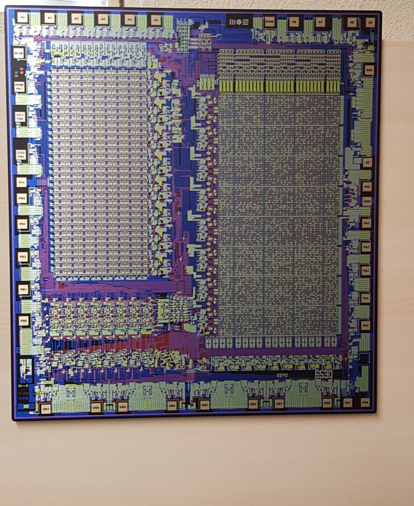
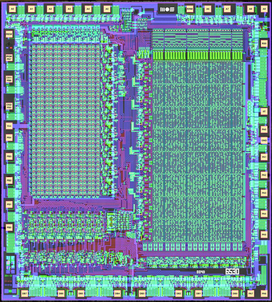
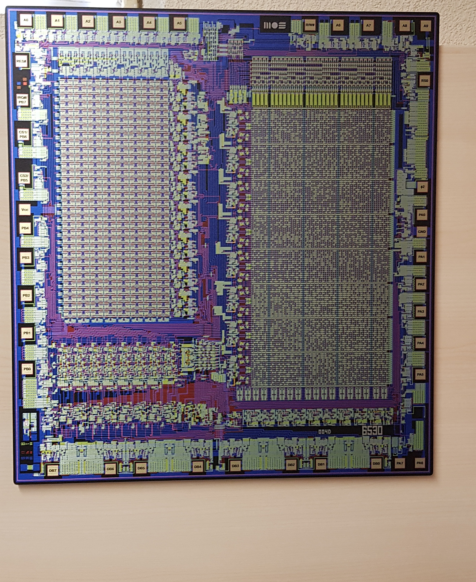
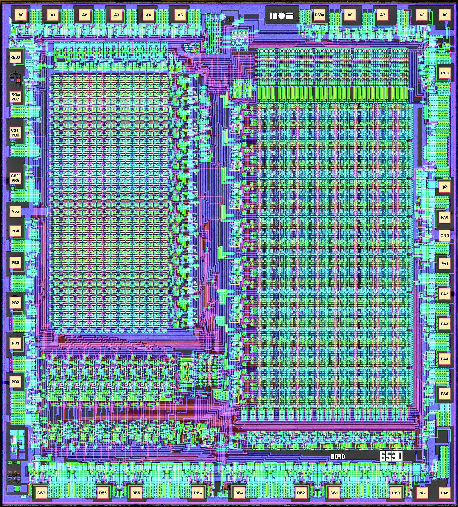
Orientation for all the chip pictures: A5 and R/W# pads are North.
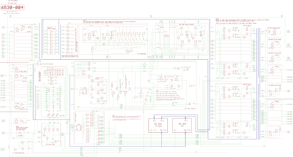
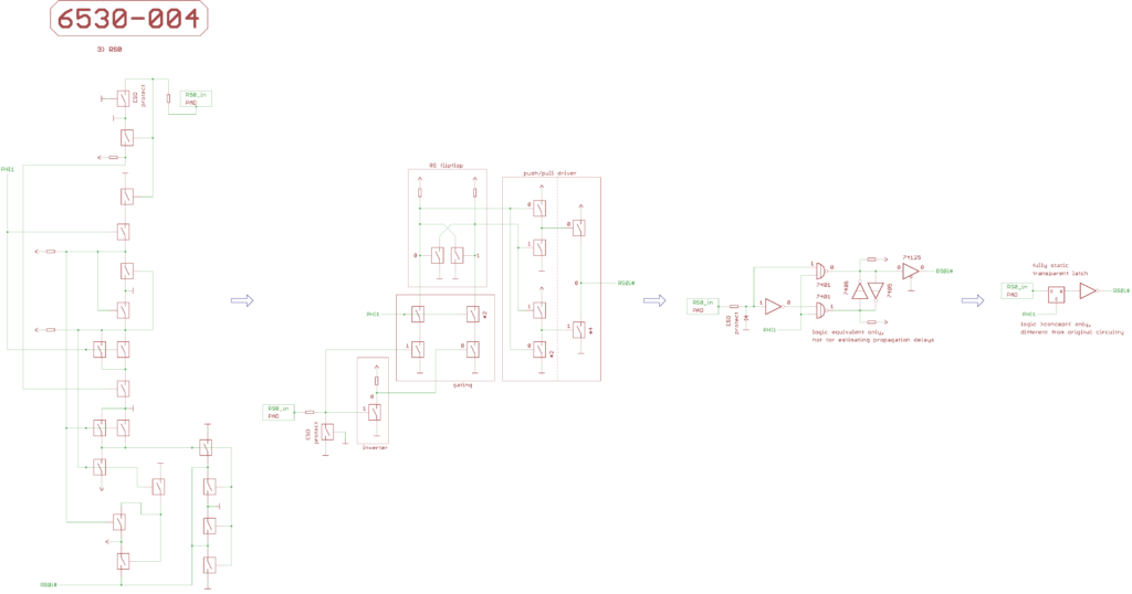
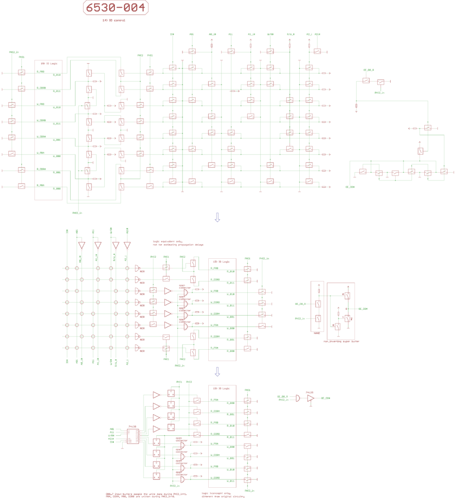
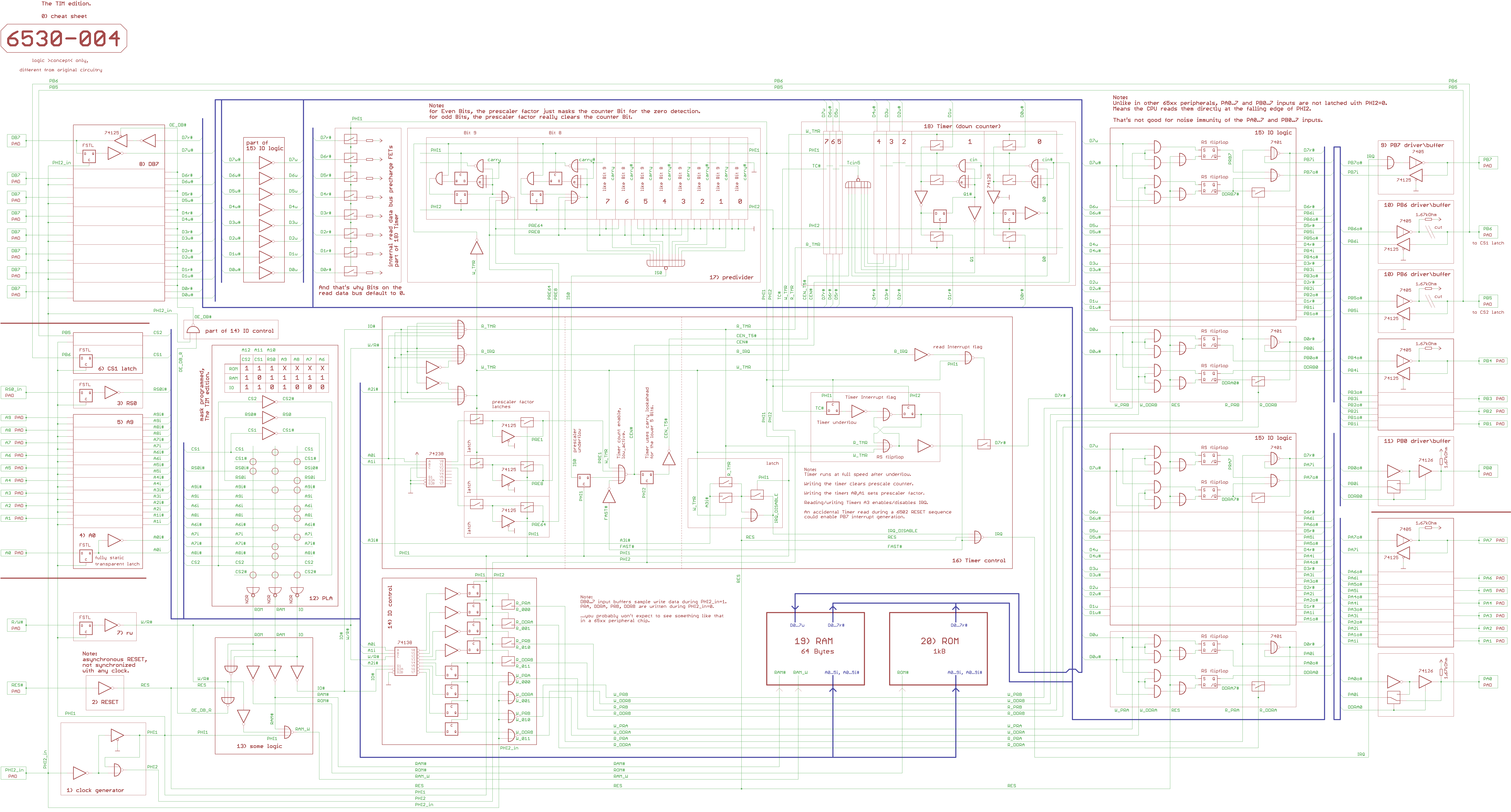
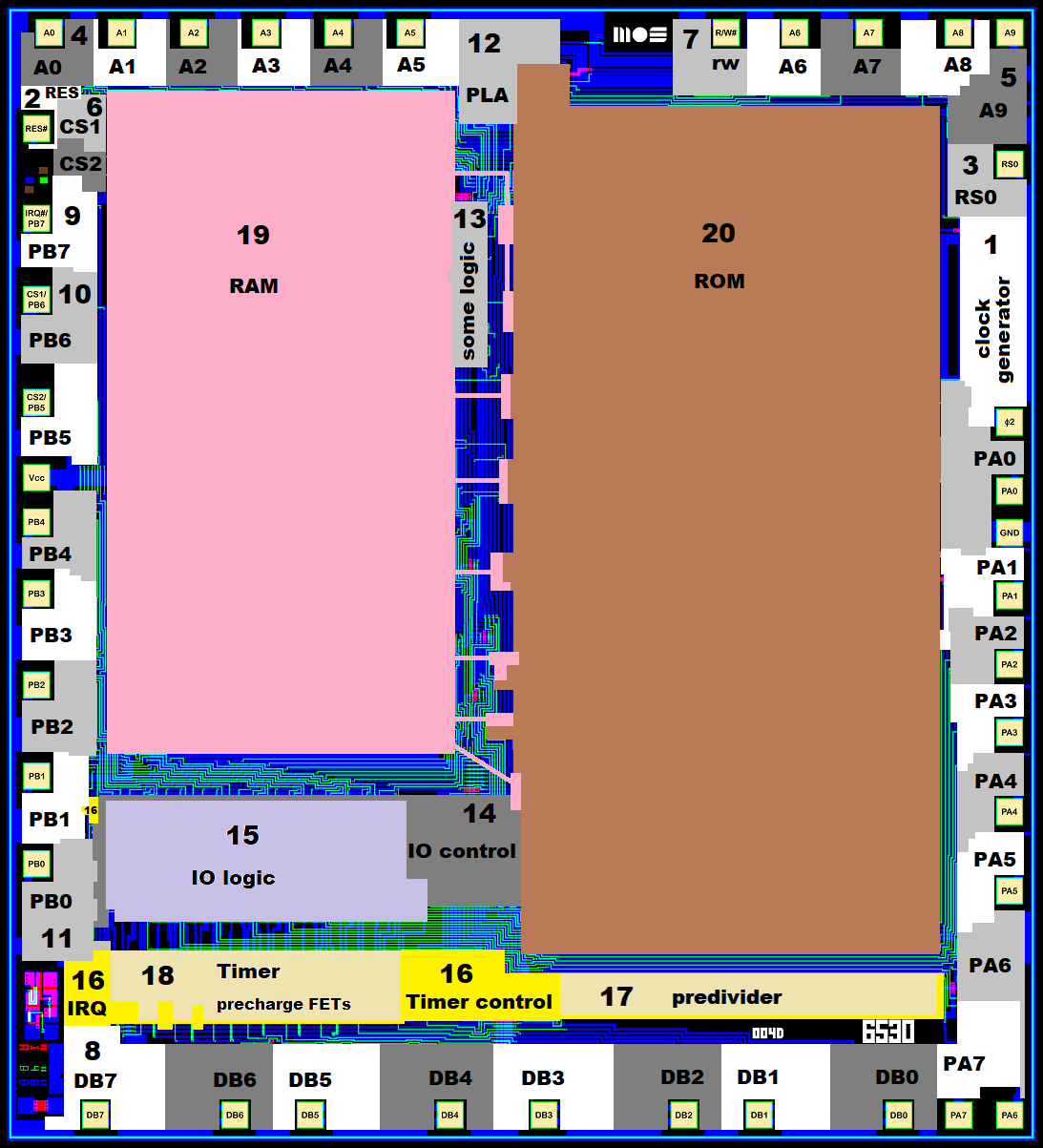
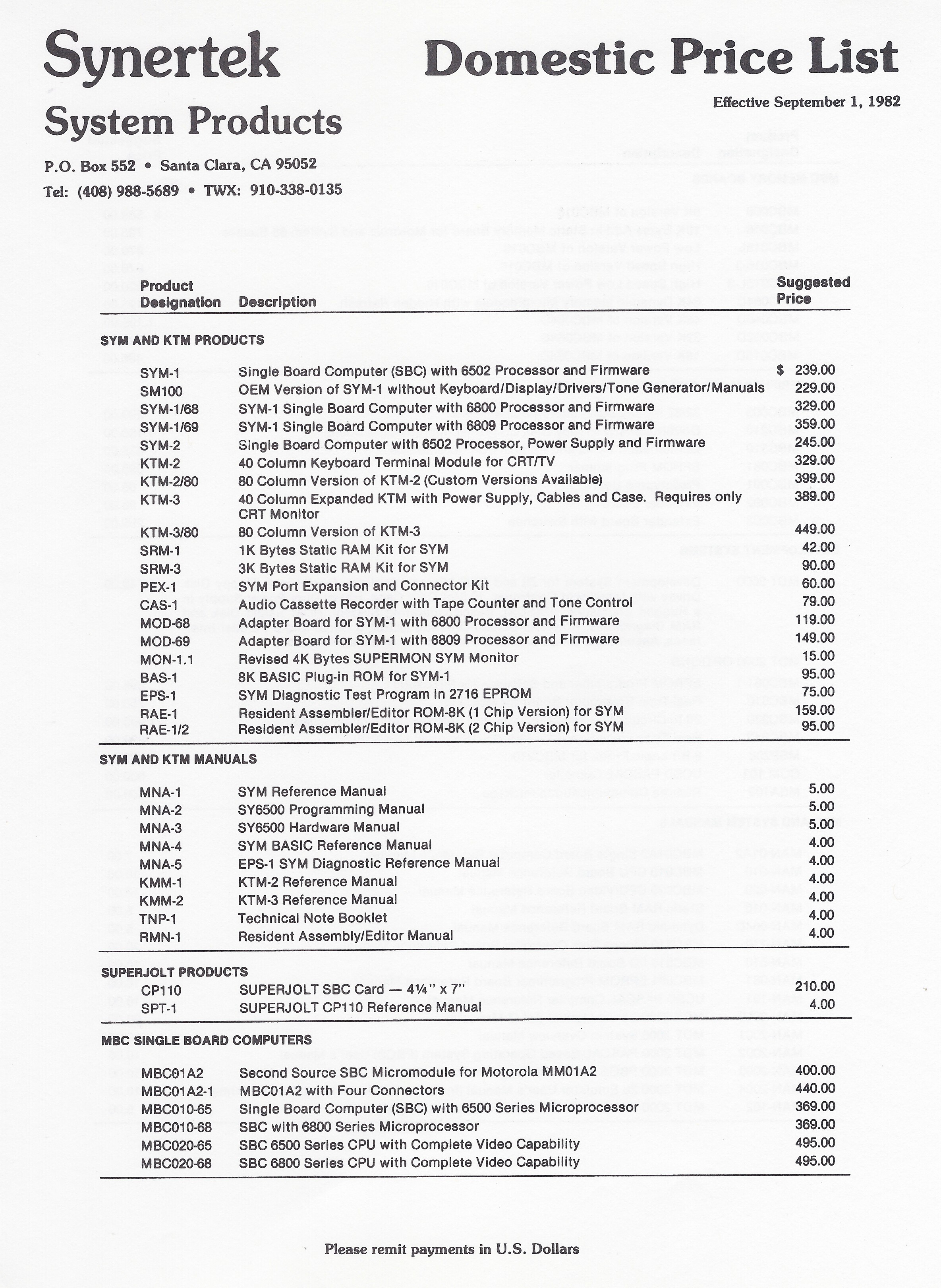
0 cheat sheet
A very simplified schematic to give an overview about what came out during the dissection.
Note:
Latches labeled FSTL are fully static transparent latches (built around a RS flipflop).
Latches not labeled FSTL are dynamic transparent latches (just a FET switch plus some trace capacitance).
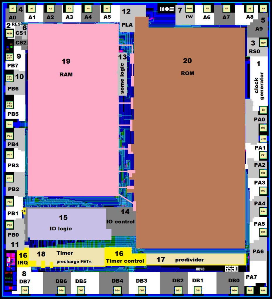
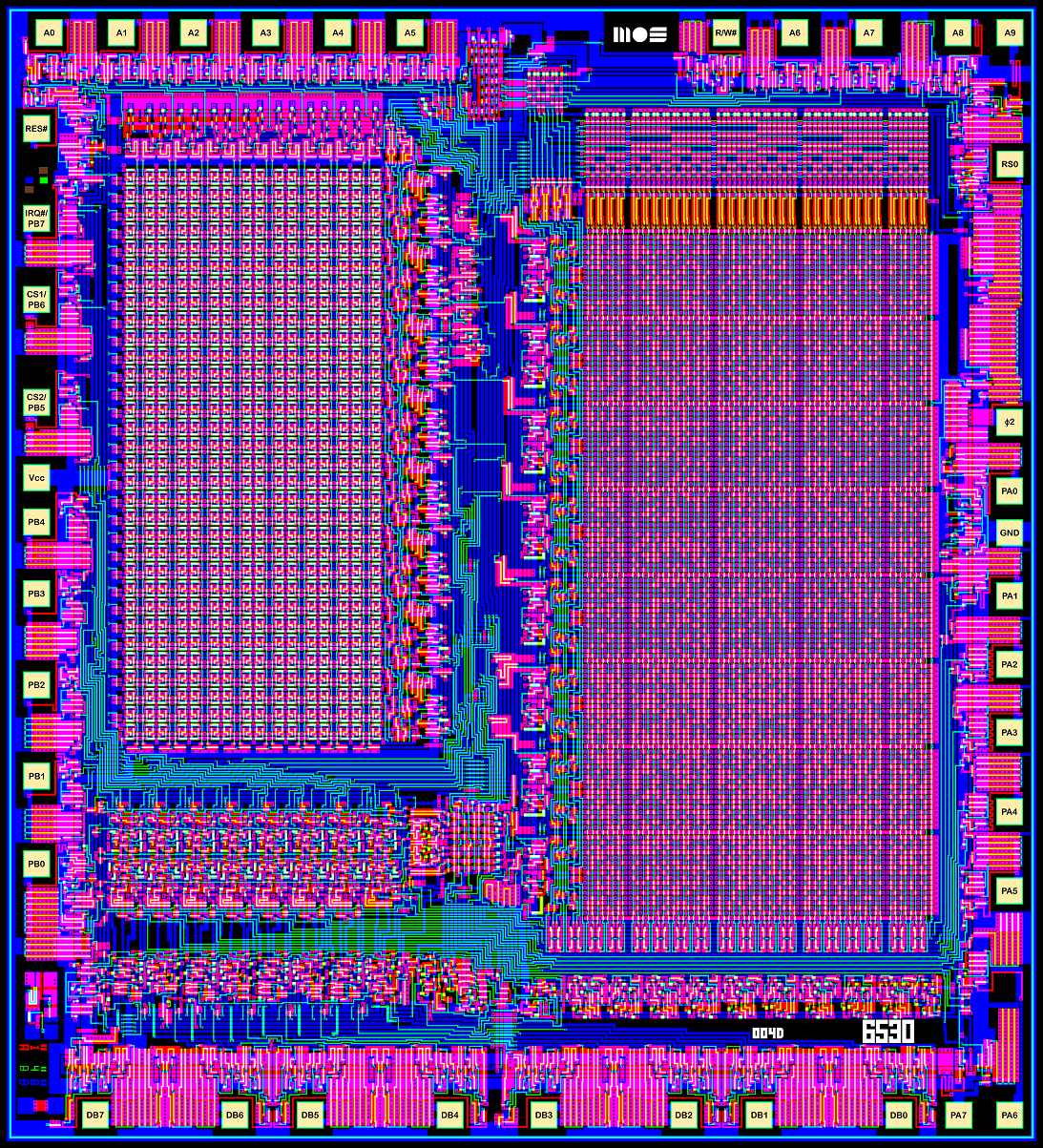
A picture of the 6530 silicon, with the interesting areas marked according to the cheat sheet.
Don’t worry because the RAM and the ROM lack any details in the cheat sheet and in this picture,
we are getting there later.
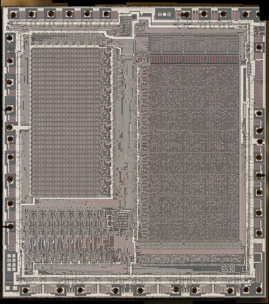
Just as a reference, another picture of the 6530 silicon without the markings.

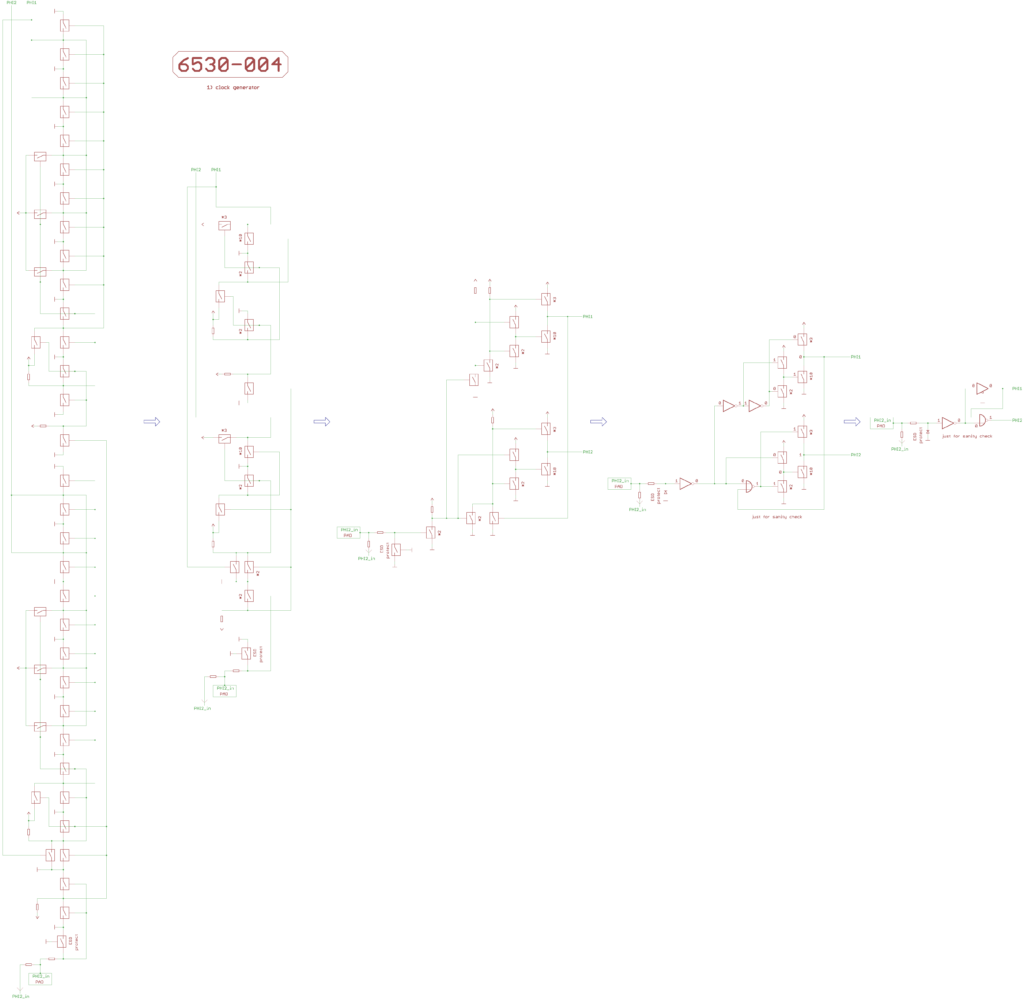
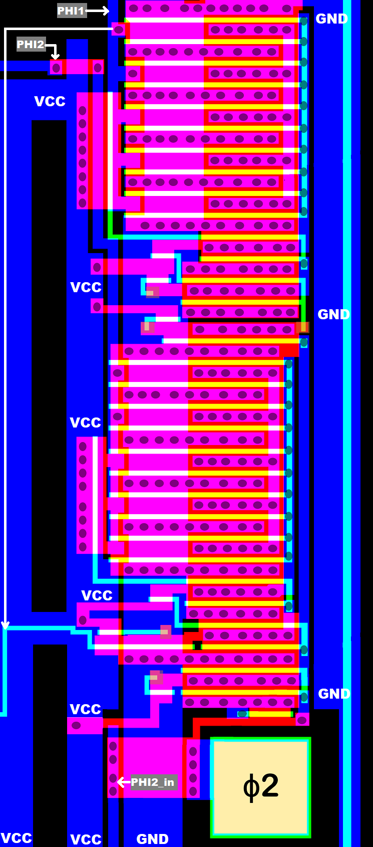
1 Clock generation
Nothing special in there.
However, it should be noted that PHI2_in also directly and unbuffered drives quite some circuitry on the chip.
6530 PHI2_in has 30pF typ. input capacitance, for a NMOS 6522 20pF typ. would be normal.
When using multiple 6530 (or 6532) chips in a system,
it probably would be a good idea to keep an eye on the total capacitive load of the 6502 PHI2 output driver
(and on the 6502 propagation delay PHI0_in to PHI2 output, which might be different for rising and falling edge of the clock).
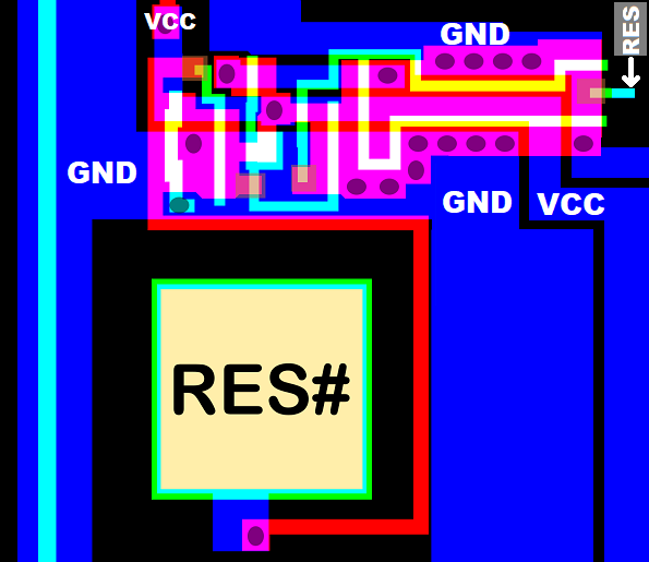
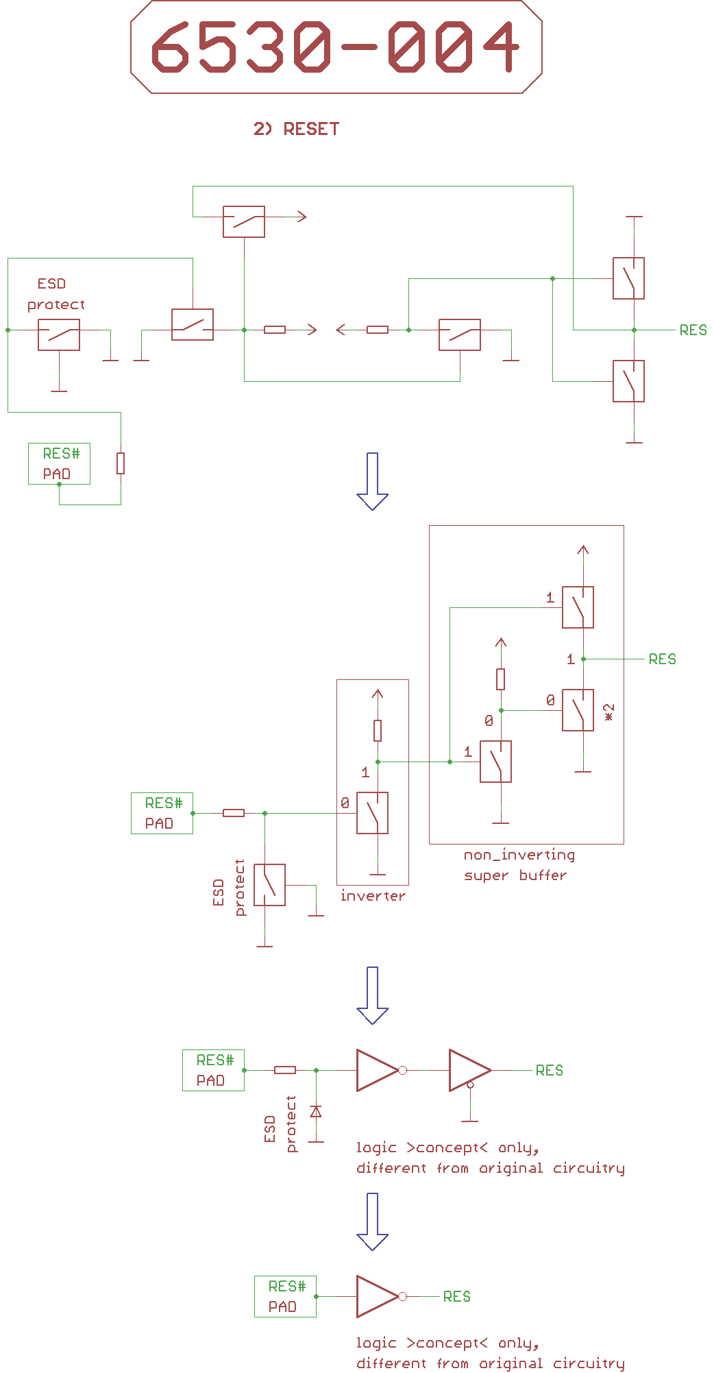
2 RESET
The low-active RES# signal from the pad goes through an inverter, then through a non-inverting super buffer,
and becomes the high_active RES signal (which puts the chip into a RESET).
Note, that the 6530 RESET is fully asynchronous, and not sampled with the clock.
Means, a glitch on RES# to logic low level at any time most likely will cause a RESET.
RES clears the PRA and PRB IO port data registers.
RES clears the DDRA and DDRB IO port data direction registers, configuring the PA0..7 and PB0..7 IO port pins as inputs.
But be aware: RES [b]does not[/b] affect the timer, the Timer Interrupt flag, the pre-scaler, and the pre-scaler factor.
RES makes sure that PB7 is not pulled low while RES is active.
RES also sets the latch for the PB7 interrupt generation to “disabled”.
But if there is something like an accidental Timer read during the RESET sequence of a 6502,
A3i could enable PB7 interrupt generation, and then there might be a falling edge on PB7 in the wrong moment…
For more details, please see “16) Timer control”.

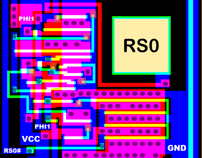
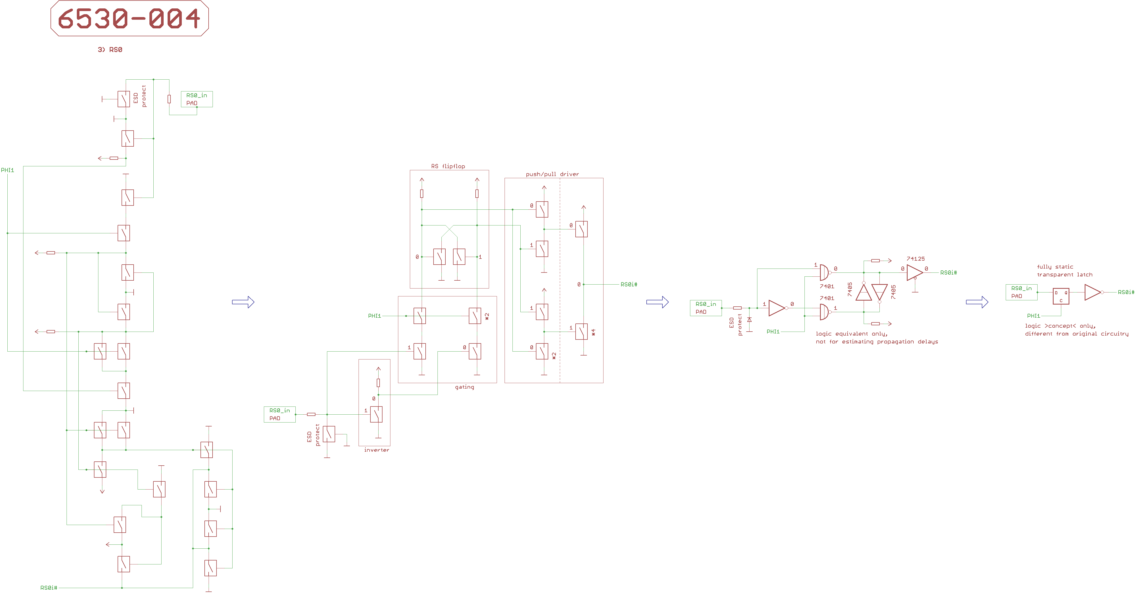
3 RS0
RS0 is an address decoder input signal.
The high-active RS0 input is sampled with PHI1 into a fully static transparent latch,
which gives out the low-active RS0i# signal that goes to the address decoder PLA.
//’i’ like in ‘Input’.
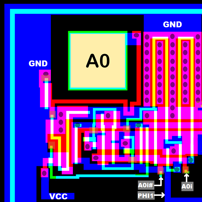
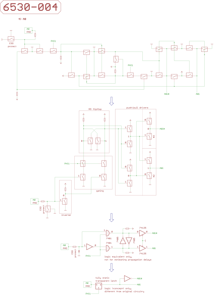
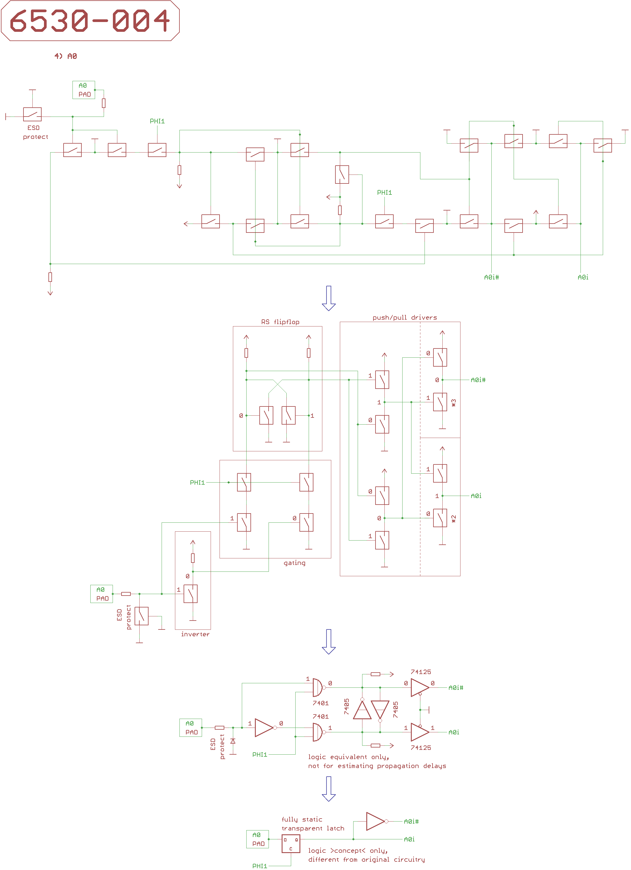
4 A0
Like RS0, high-active A0 from the pad is sampled with PHI1 into a fully static transparent latch.
A special thing is, that the latch feeds push/pull output drivers which generate
the low-active A0i# and the high-active A0i.
When taking a look at the chip layout, it appears that big transistors are located between the address pads.
They somehow look like output drivers (for external signals) to be found in other chips,
but they are driving the internal address lines inside the chip instead.
I think it’s a good/clever idea to re-use an output driver structure/topology for driving internal address lines
to deal with the capacitances build up by the RAM and ROM address decoders.
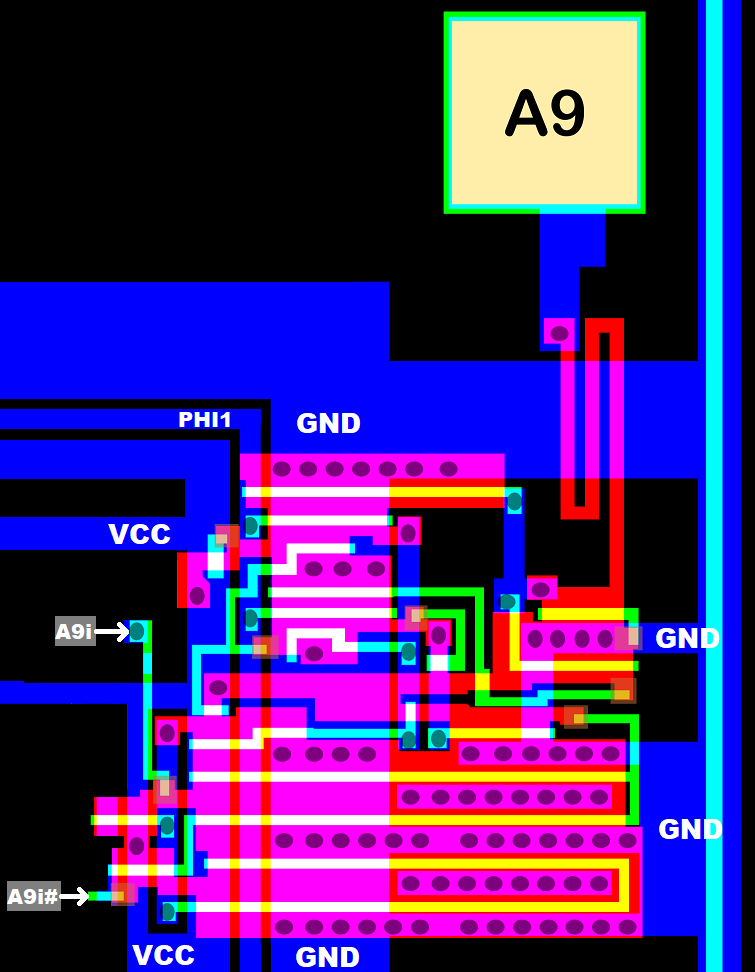
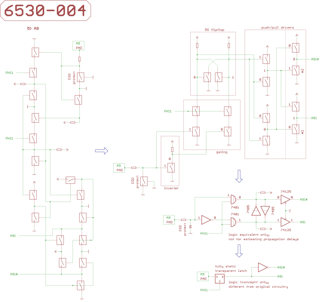
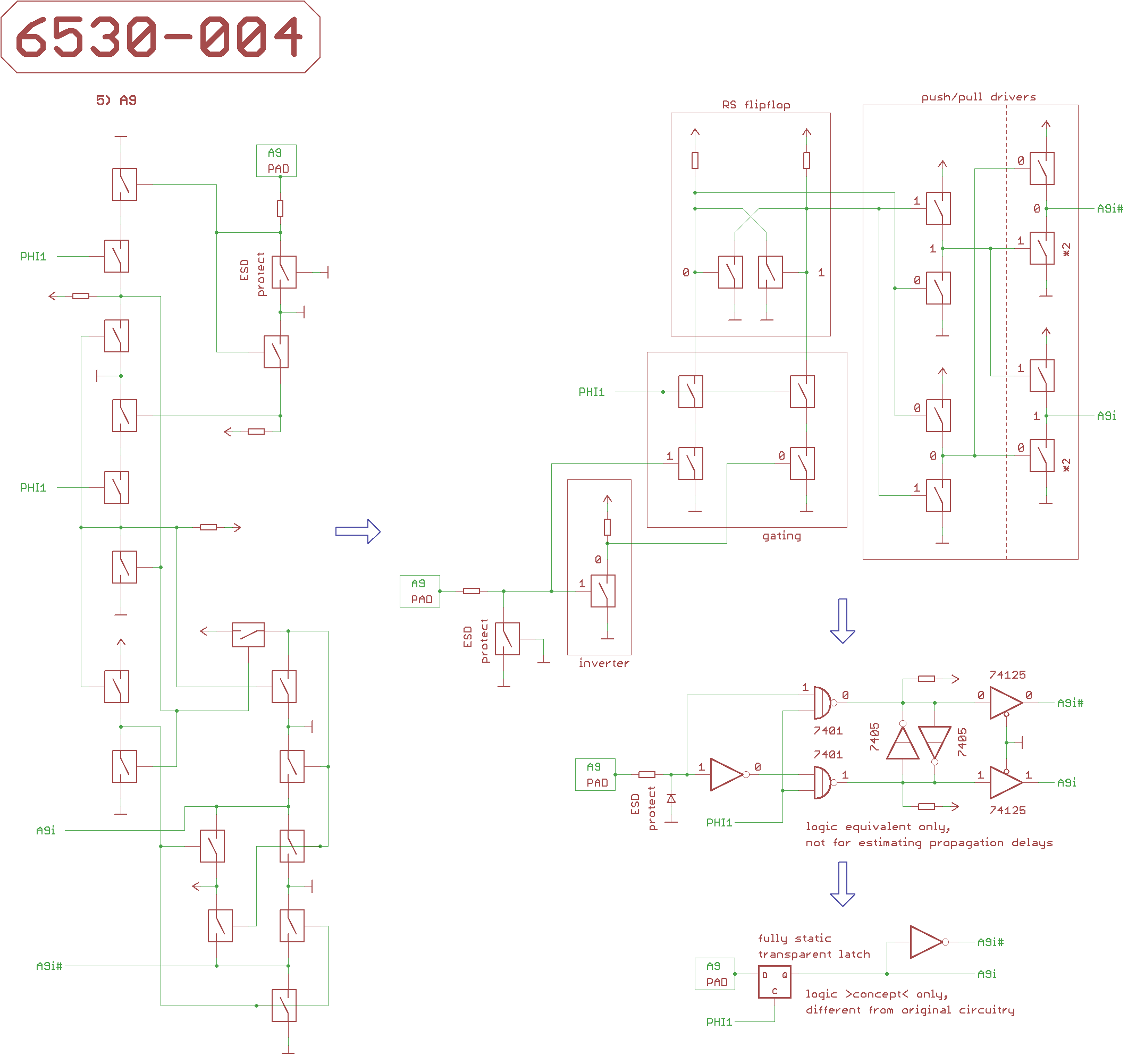
5 A9
Since the A9 input buffer circuitry layout is different from A0,
I felt a need to take a closer look at it,
but from the logic design point of view the input circuitry for A0 and A9 is identical.
Layout of the A1..A5 input circuitry is identical to A0.
Layout of the A6, A7 input circuitry is identical to A0, but it’s mirrored to make better use of chip space.
Layout of the A8 input circuitry is a variation of A9.
Now for a list of signals generated by the A0..A9 output drivers:
West to East: A0i#, A0i; A1i#, A1i; A2i#, A2i; A3i#, A3i; A4#i, A4i; A5i#, A5i; A6i, A6i#; A7i, A7i#; A8i, A8i#;
North to South:
A9i,
A9i#
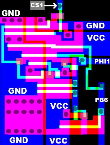
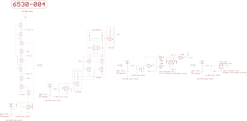
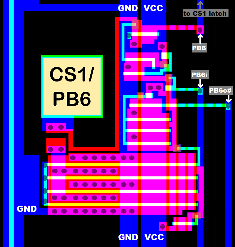
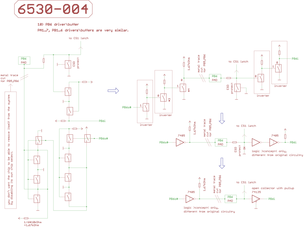
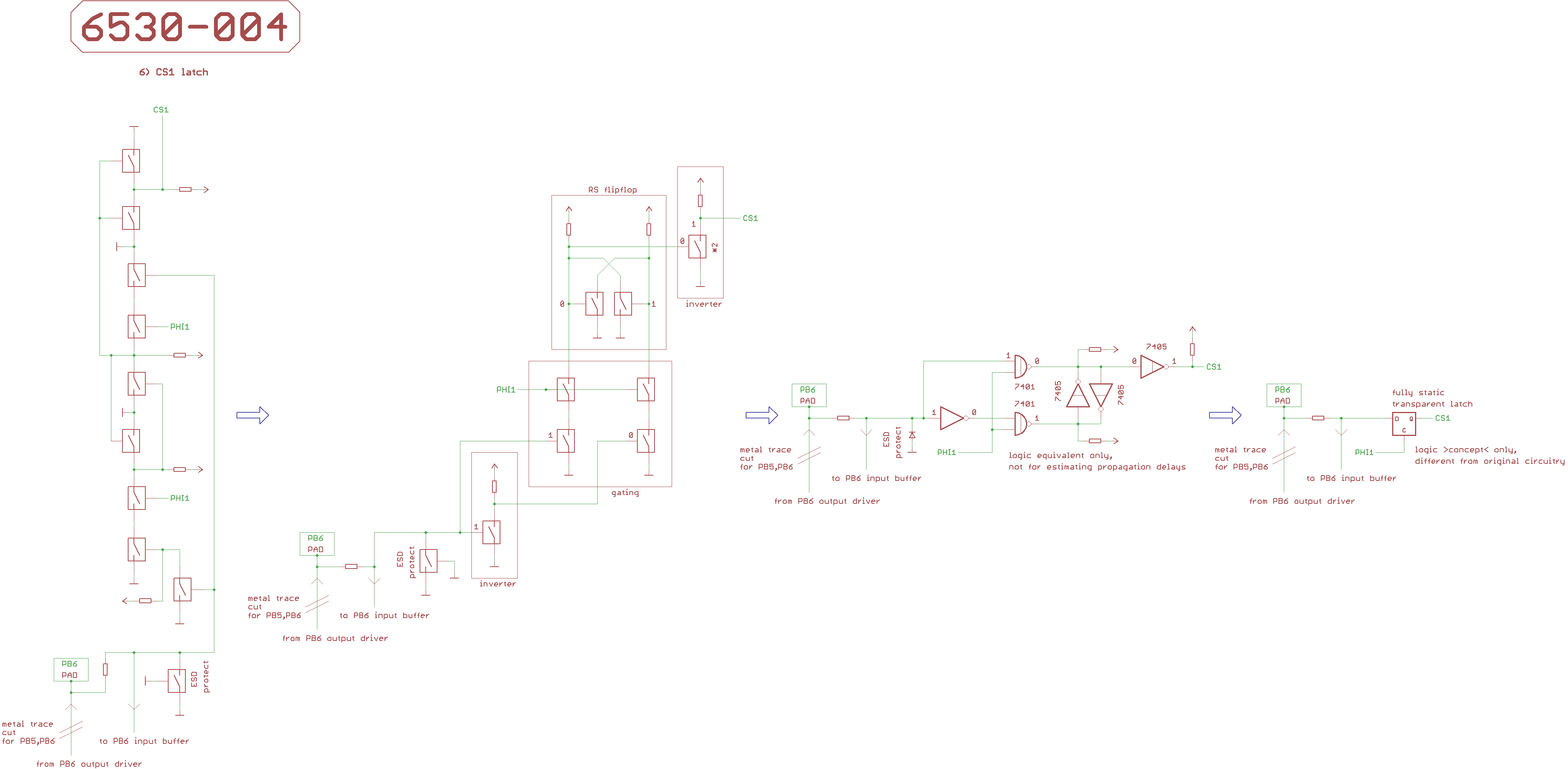
6 CS1 latch
The CS1 latch is a fully static transparent latch, which samples PB6 at PHI1,
and gives out the high_active CS1 signal to the address decoder PLA.
Similar to the CS1 latch,
the CS2 latch also is a fully static transparent latch, which samples PB5 at PHI1,
and gives out the high_active CS2 signal to the address decoder PLA.
Both latches are located between the RES# pad and the RAM block
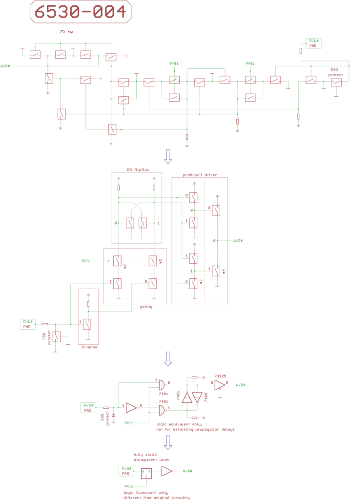
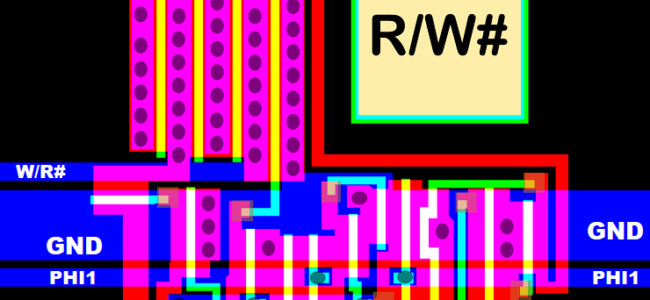
7 R/W#
R/W# (high=read, low=write) is sampled with PHI1 into a fully static transparent latch,
which feeds a push/pull driver generating W/R# (high=write, low=read)

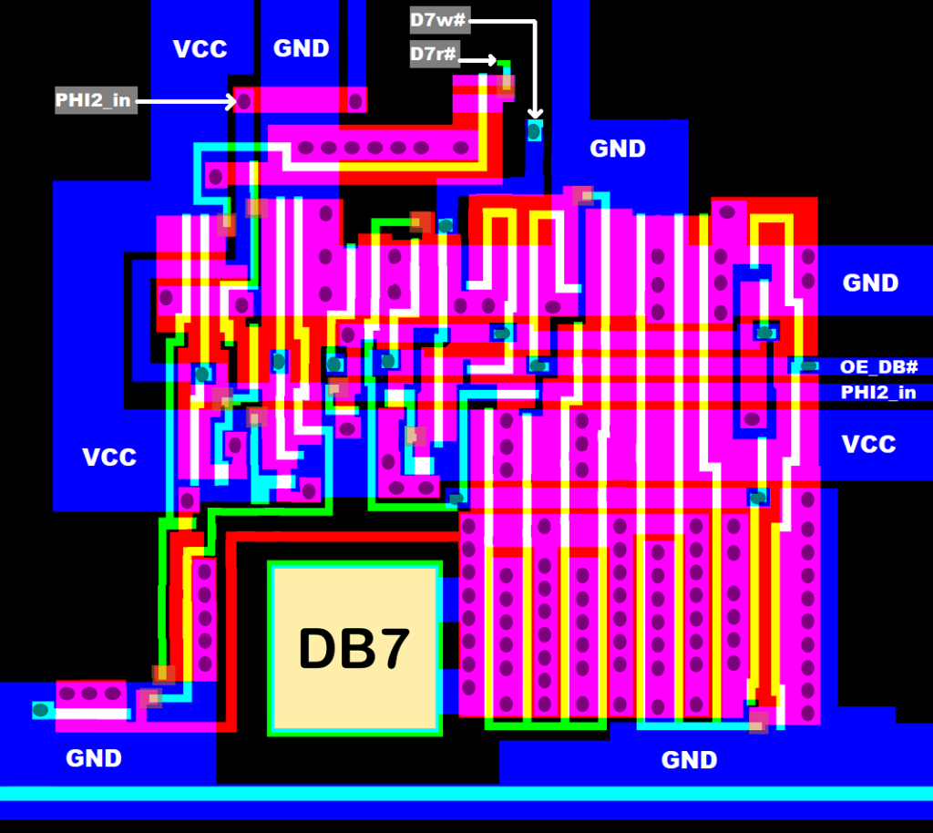
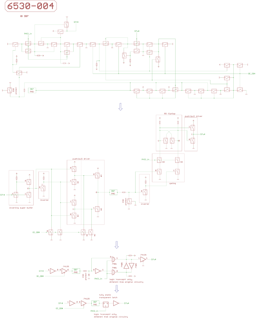
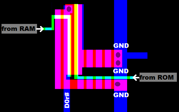
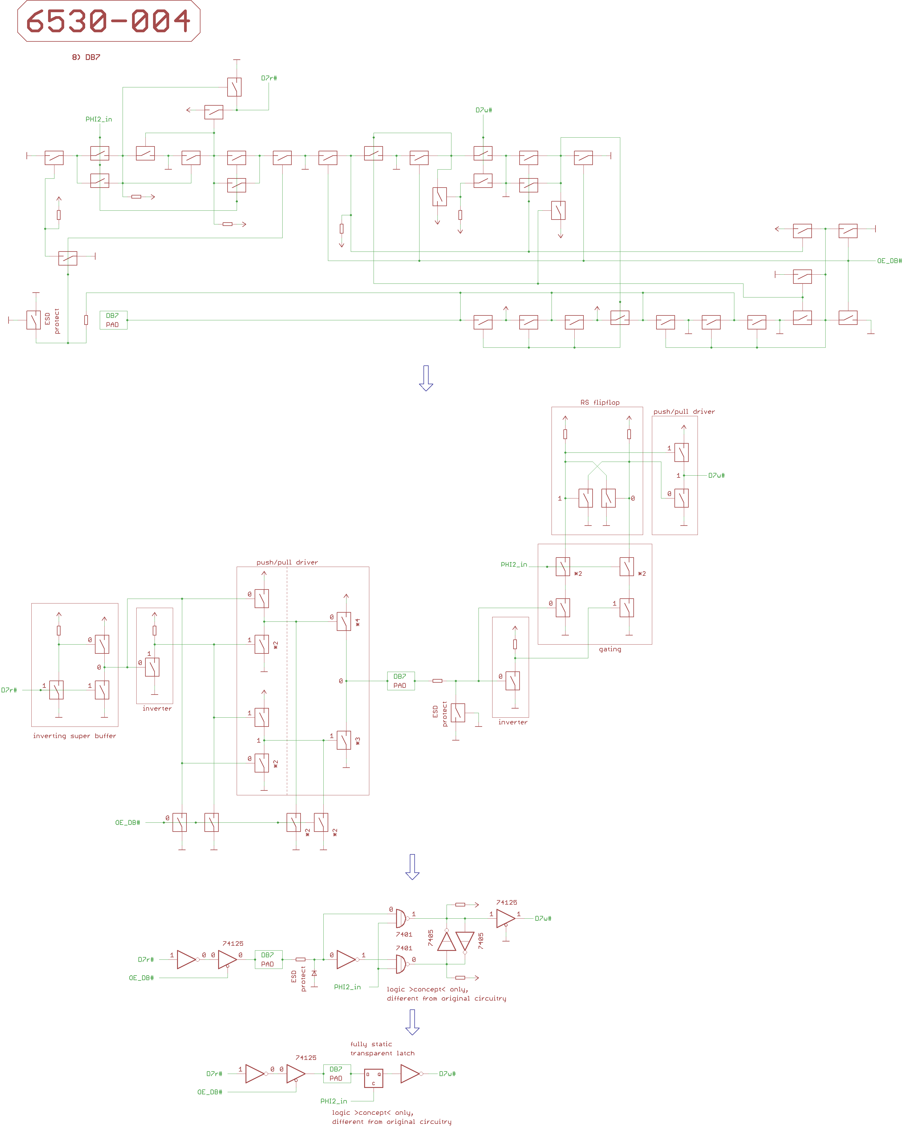
8 DB7
Overview:
DB0..7 external data bus pads (high_active).
Internal write data bus D0..7w# (low-active) when writing registers.
//Internal write data bus D0..7w (high_active) is generated by super buffers located South in the IO logic block.
Internal read data bus D7r# (low-active) when reading registers.
//The read data bus is pre-charged during PHI1 with FETs located South in the Timer block.
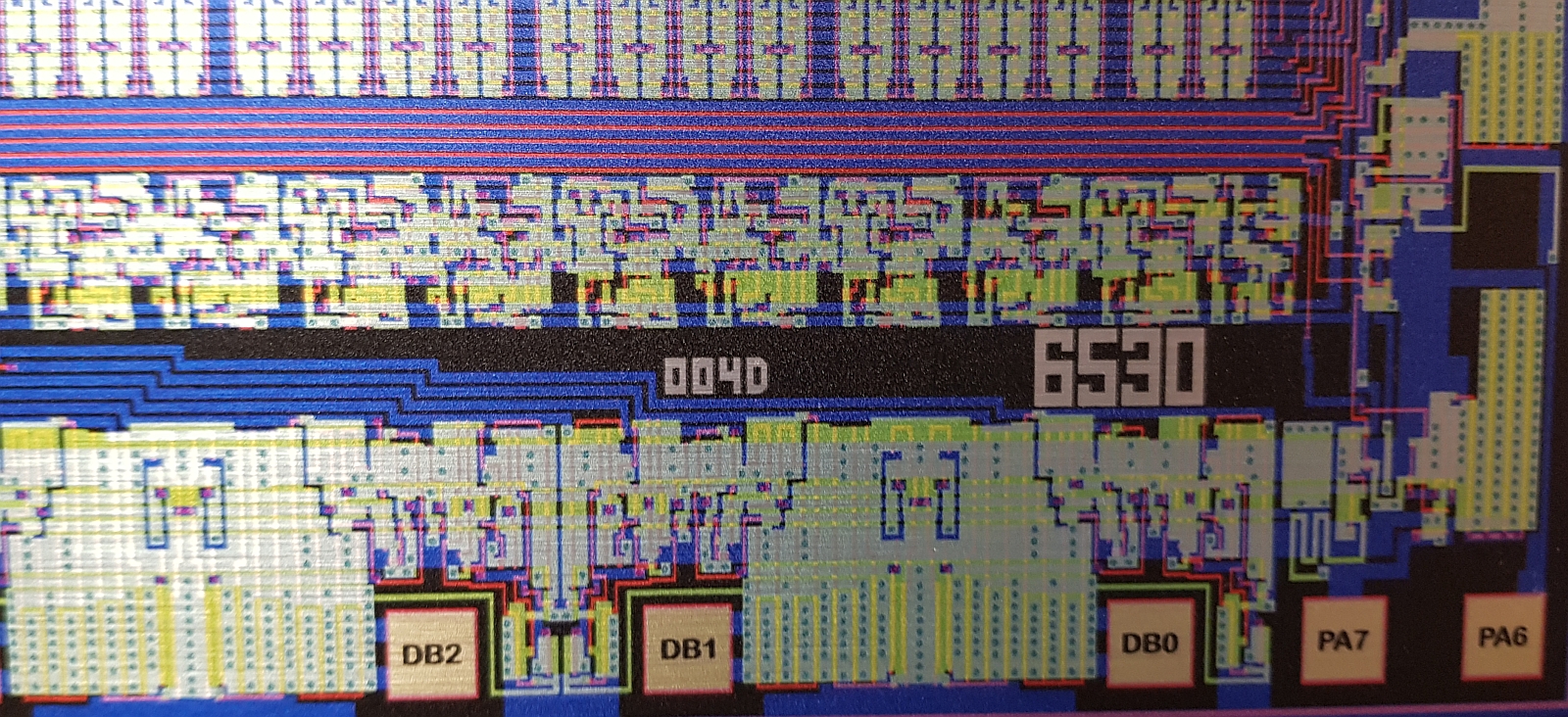
Layout for the DB0..6 circuitry is pretty similar to DB7, so we only take a look at DB7.
On the input side, the high_active DB7 pad is sampled with PHI2_in into a fully static transparent latch,
which feeds a push/pull driver generating the low-active D7w# signal for the write data bus.
//Note, that the PHI2_in signal controlling the DB0..7 latches comes directly and unbuffered from the PHI2_in pad.
On the output side, the low-active OE_DB# control signal enables the inverting DB7 push/pull driver
which takes the low-active D7r# signal from the read data bus and emits it in high_active form
on the external DB7 data bus pad.
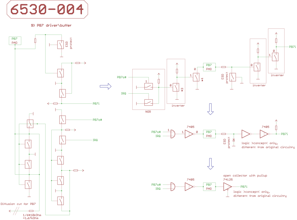
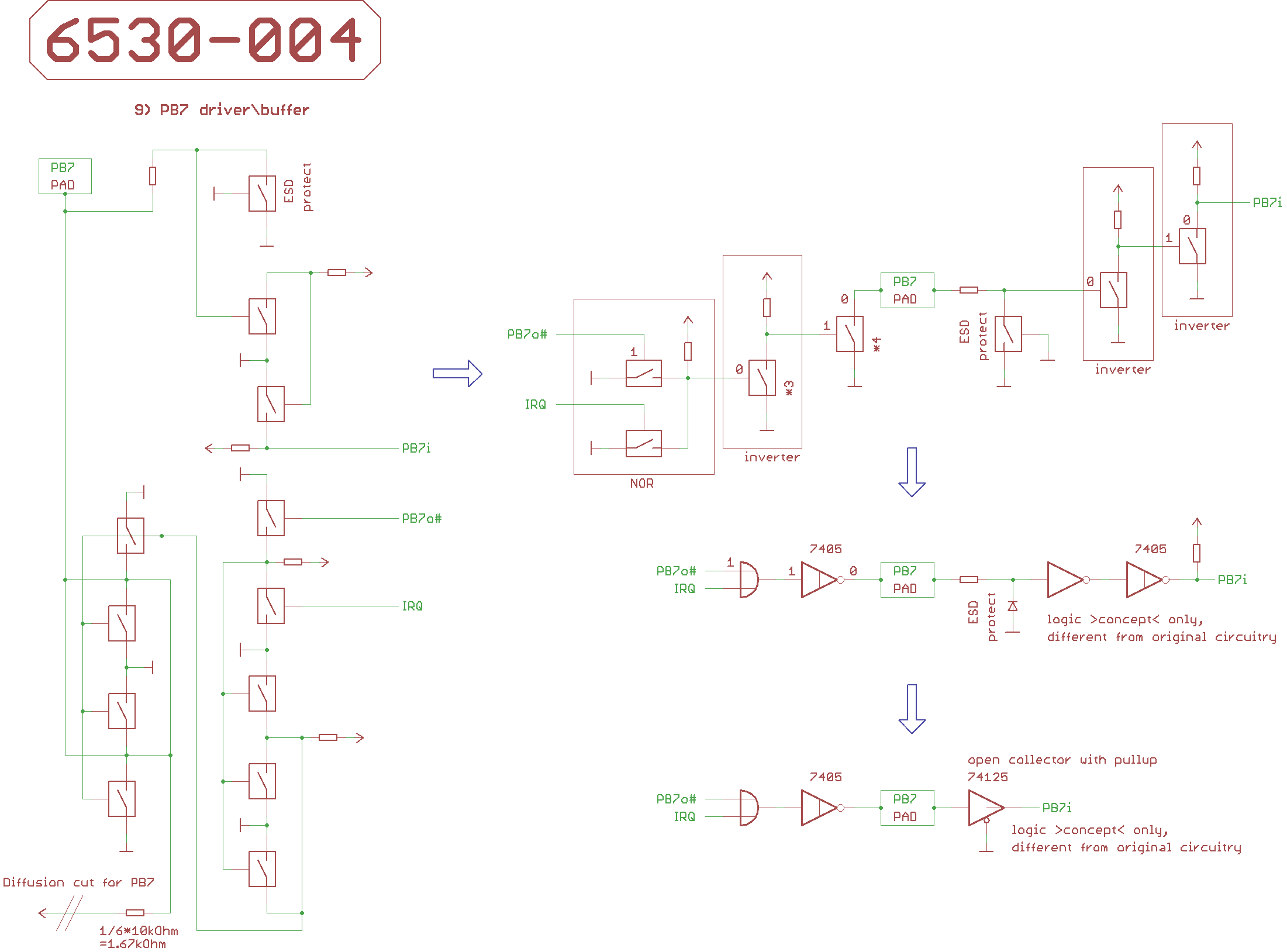
9 PB7
PB7 is an open drain IO port signal, which lacks a pull-up resistor.
In addition to being an IO port signal,
it also works as a (low-active) Timer overflow interrupt output,
supposed to be tied to the IRQ# pin of a 6502.
The PB7 pull-up resistor (FET) is present in the chip layout,
but the diffusion layer between the pull-up and VCC is cut.
I think that’s because if the PB7 pads of multiple 6530 chips are tied to IRQ#,
and every 6530 would have a PB7 pull-up resistor,
the resulting impedance of all the PB7 pull-up resistors in parallel on the IRQ# line
would be too low for a 6530 PB7 output driver to pull down IRQ# to a logic low level.
Not much to say on the output side:
if PB7o# is high OR IRQ is high, the output driver pulls PB7 low.
//For logic high level, you need to add an external pull-up resistor between PB7 and VCC.
In the IO logic block, PB7o# is the output of a NOR gate fed by data bit PRB7 and data direction Bit DDRB7#.
If PRB7=0 (data Bit low) and DDRB7=1 (PB7 is output), PB7o# is high, and PB7 is pulled to GND.
The high_active IRQ signal is generated in the Timer control block.
//IRQ can be enabled/disabled with A3 during Timer reads/writes.
If it’s enabled AND if the Timer Interrupt flag is set, IRQ is high, and PB7 is pulled to GND…
…by ignoring the PRB7 and DDRB7 Bits.
On the input side, the PB7 pad signal goes through two inverters, becomes PB7i and goes to the IO port logic,
IO port logic places it in inverted form on the D7r# read data bus when reading data register PRB,
we are getting there later.
Note, that the PA0..7 and PB0..PB7 input signals are not latched at PHI1, the CPU reads them directly,
we are getting there later, too.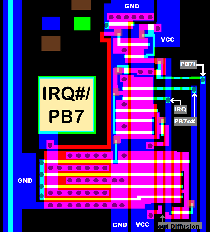
10 PB6
PB6 pad also feeds CS1 latch, PB6 pad also feeds CS2 latch,
CS1 and CS2 are used in the (mask programmed) address decoder PLA of the chip we had dissected,
and as a mask programmed option the metal trace between PB5,PB6 pad and PB5,PB6 driver is cut.
//You don’t want the chip to be able to remove itself from the system by disabling its own chip select.
PA1..7 and PB1..6 pad circuitry is pretty similar to PB7.
They are open drain outputs with pull-up resistor (FET).
So we just focus on PB6:
On the output side, if PB6o# is high, and if the metal trace wouldn’t be cut, the output driver would pull PB6 low.
In the IO logic block, PB6o# is the output of a NOR gate fed by data bit PRB6 and data direction Bit DDRB6#.
If PRB6=0 (data Bit low) and DDRB6=1 (PB7 is output), PB6o# is high.
On the input side, the PB6 pad signal goes through two inverters, becomes PB6i and goes to the IO port logic,
IO port logic places it in inverted form on the D6r# read data bus when reading data register PRB,
we are getting there later.
Note, that the PA0..7 and PB0..7 input signals are not latched at PHI1, the CPU reads them directly,
we are getting there later, too.
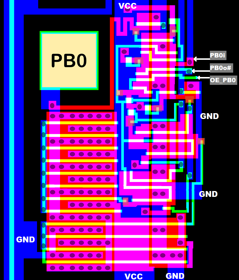
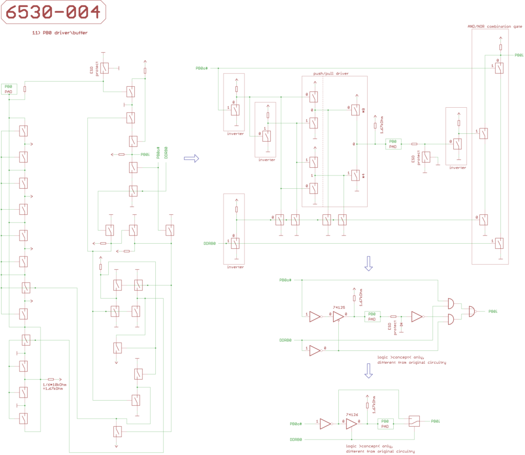
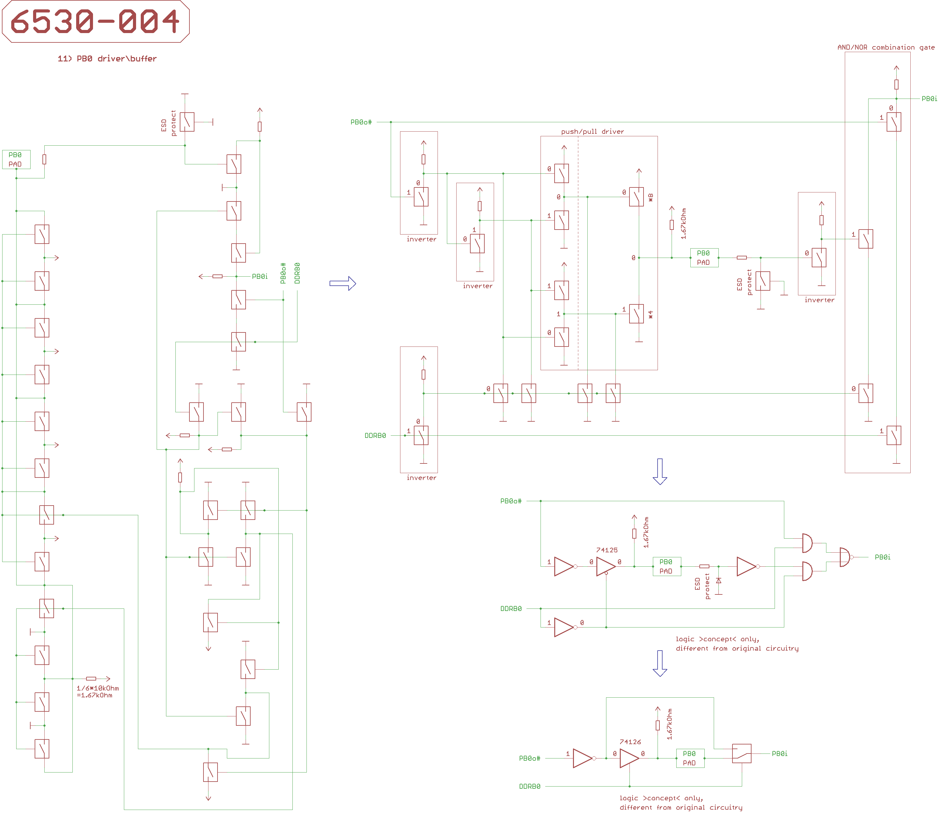
11 PB0
PA0 and PB0 have a pull-up resistor (FET),
but unlike PA1..7 and PB1..7, PA0 and PB0 have true push/pull output drivers.
PA0 and PB0 are meant to source 3mA for driving darlington transistors and such.
PA0 and PB0 circuitry layout is different to make better use of chip space,
but electrically they are identical, I checked.
So we now focus on PB0.
On the output side:
PB0 output driver is enabled by DDRB0=1 (when PB0 is configurated as an output).
PRB0# which goes into the output driver is the low-active output signal of the PRB0 data register Bit.
When DDRB0=1:
If DDRB=1 and PRB0=0 (PRB0#=1), the output driver pulls PB0 low.
If DDRB=1 and PRB0=1 (PRB0#=0), the output driver pulls PB0 high.
And that’s all there is to it.
The input side is more complicated:
There is a danger that the voltage at PB0 doesn’t reach logic high level
when the PB0 driver has to source a lot of current.
That’s why we have sort of a 2:1 multiplexer controlled by DDRB0 (data direction register Port B).
The multiplexer generates PB0i, which goes to the IO port logic,
IO port logic places it in inverted form on the D0r# read data bus when reading data register PRB,
we are getting there later.
If PB0 is configurated as an input, PB0i is generated from the PB0 pad.
If PB0 is configurated as an output, PB0i is generated from the data register Bit PRB0.
//I’m simplifying things a bit here.
Note, that the PA0..7 and PB0..7 input signals are not latched at PHI1, the CPU reads them directly,
we are getting there later, too.
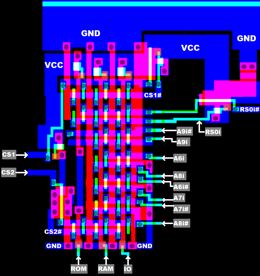
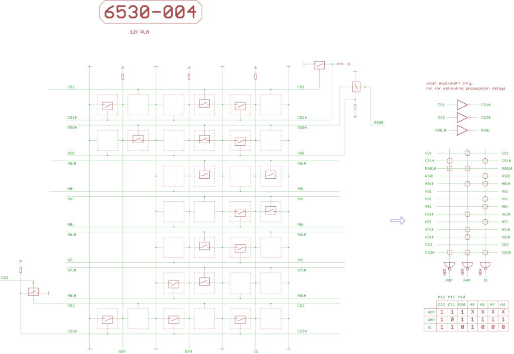
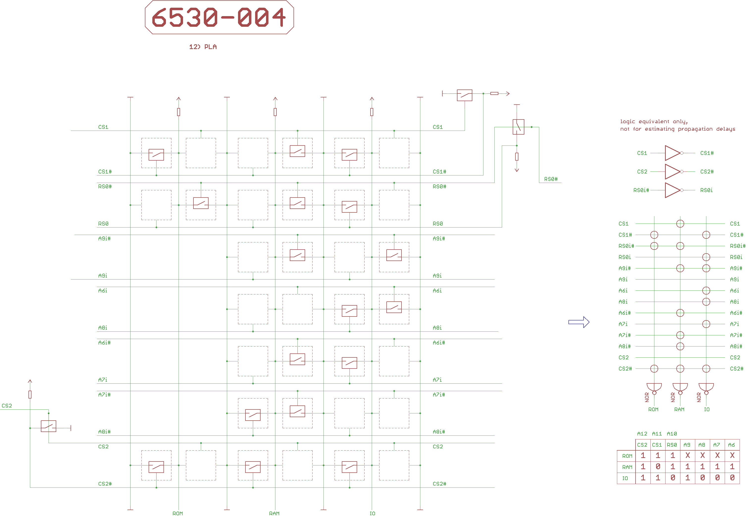
12 PLA
(mask) programmed logic array (PLA), also known as “the address decoder”.
Mask programmed as in “customer specific”.
It decides, where ROM, RAM and IO (including Timer) show up in the 6502 address space.
Located high up North, between A5 pad and R/W# pad.
Basically, we have three NOR gates:
One for selecting ROM: fed by CS1, CS2, RS0i. //CS1#, CS2#, RS0i# respectively.
One for selecting RAM: fed by CS1, CS2, RS0i, A6..9i. //CS1#, CS2#, RS0i#, A6..9i# respectively.
One for selecting IO: fed by CS1, CS2, RS0i, A6..9i. //CS1#, CS2#, RS0i#, A6..9i# respectively.
Where CS2 is supposed to be A12, CS1 is supposed to be A11, and RS0 is supposed to be A10.
//The A0..9 input buffers emit A0..9i (high_active) and A0..9i# (low-active).
We have three inverters, generating CS1# from CS1, CS2# from CS2, and RS0i from RS0i#.
For those who are new to the game:
In the polygonized chip picture, red is diffusion layer, green is PolySi layer, blue is metal layer.
Where ever green crosses red, that’s the active region of a FET, and green is the Gate of that FET.
So the PLA was mask programmed by changes in the diffusion layer.
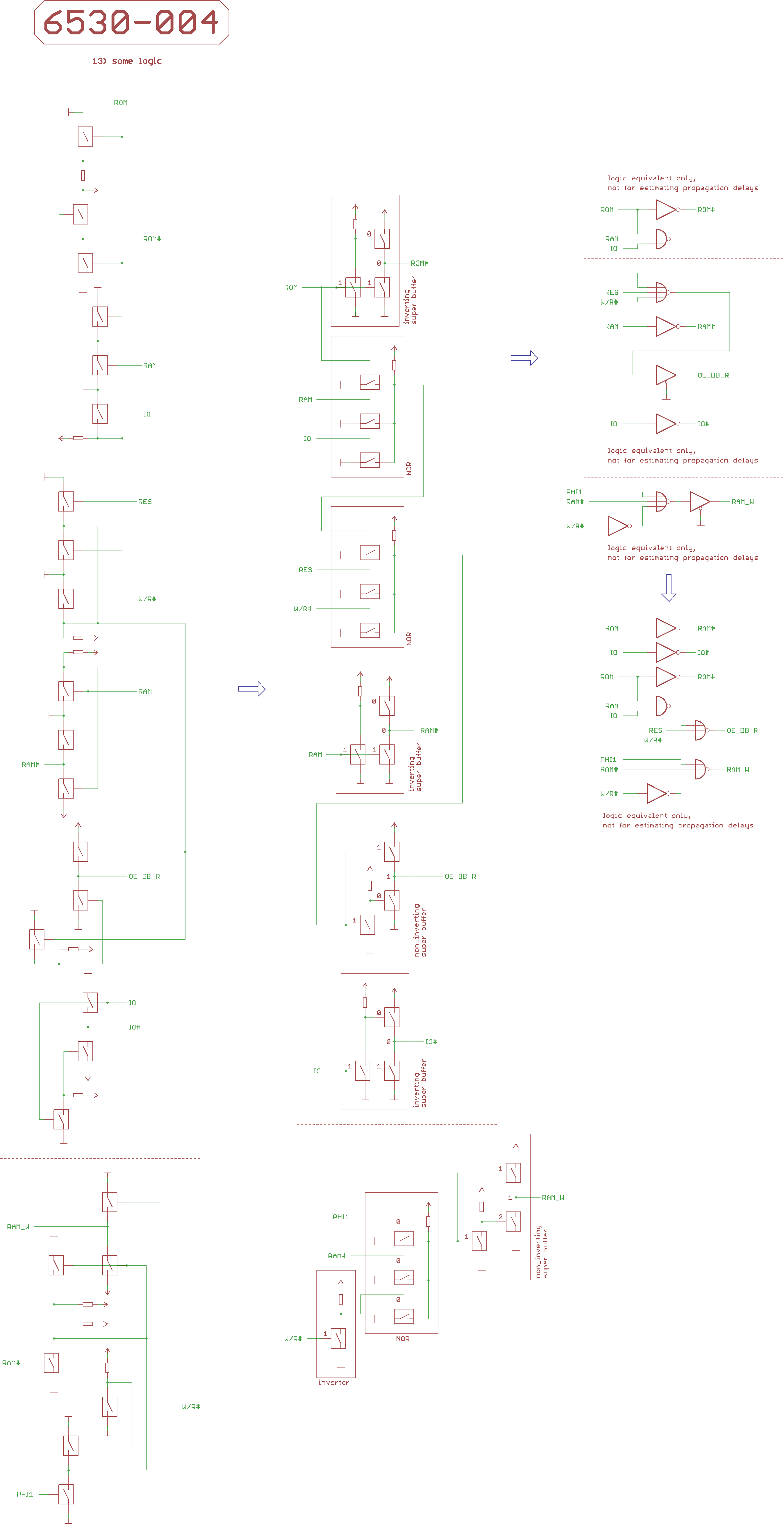
13 some logic
A tangled mass of logic gates located North East from the RAM, between RAM and ROM.
It generates ROM# (low-active) from ROM (high-active), RAM# from RAM, IO# from IO.
Also, it generates RAM_W (high_active), the RAM write enable signal,
which is 1 when PHI1=0 (what is different from “when PHI2=1”), AND when RAM is selected, AND when W/R#=1 (write).
Also, it generates OE_DB_R (high-active), which is 1 when ROM OR RAM OR IO is selected, AND when RES is inactive, AND when W/R=0 (read).
In 14 IO control, there is a NAND gate fed by OE_DB_R and PHI2_in which generates the low-active OE_DB# signal.
OE_DB# enables the DB0..7 output drivers.
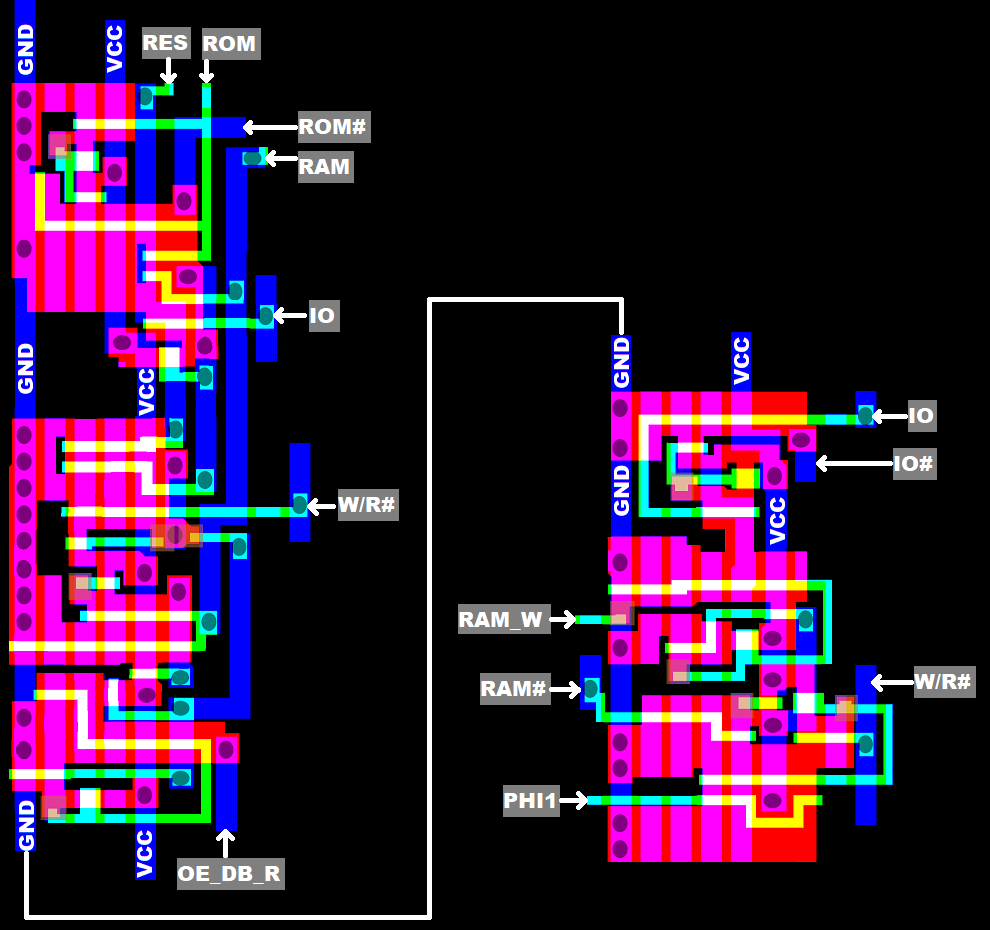

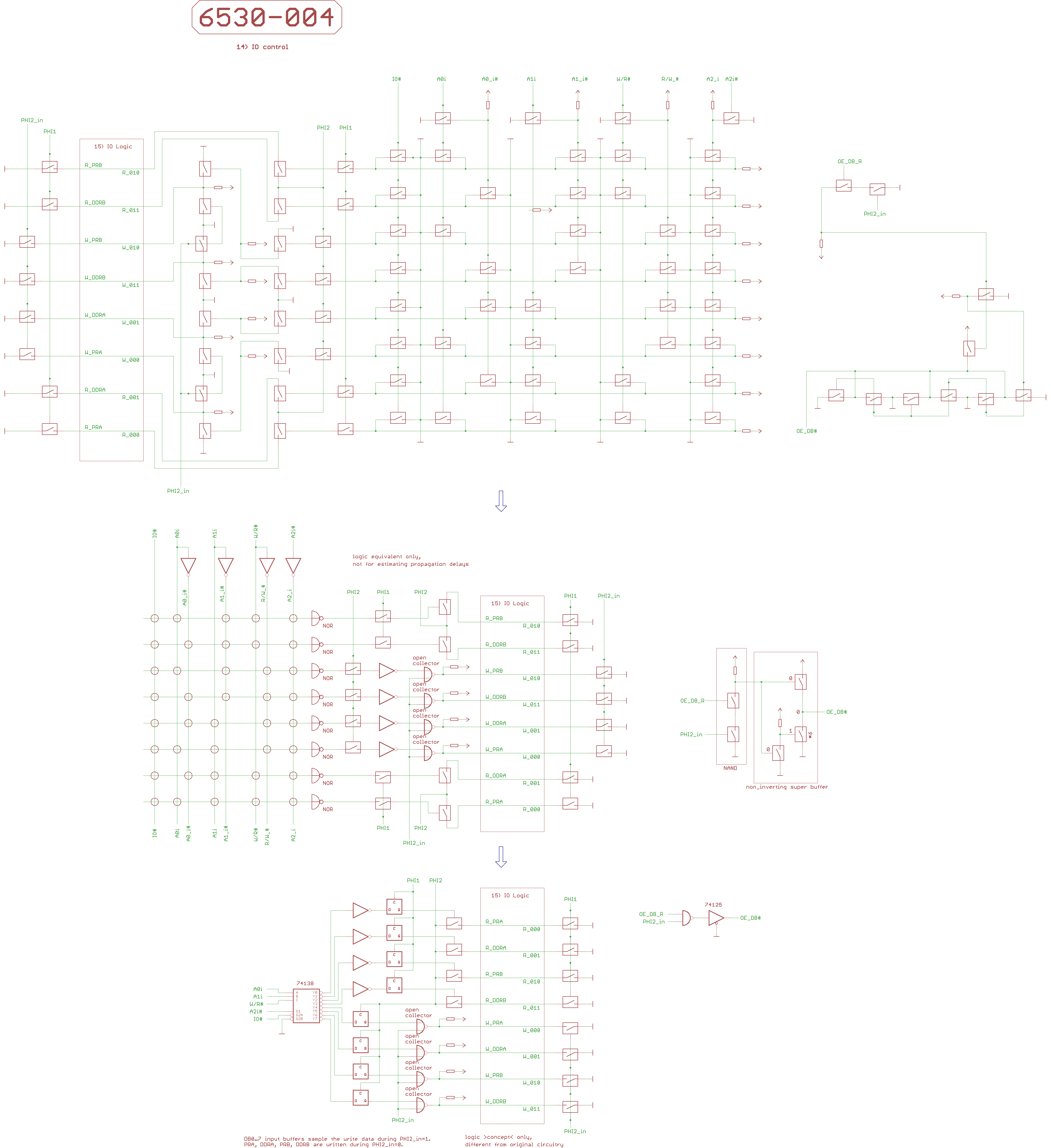
14 IO control
The IO control block is located below the South East corner of the RAM, East of the IO logic block.
It generates the read/write control signals for the IO logic.
First, we have a PLA like structure (containing 8 NOR gates), which is enabled when IO#=0 and A2i#=1.
According to A0i, A1i and W/R#, it generates 4 read signals and 4 write signals.
The 4 read signals from the “IO control PLA” are sampled with PHI1 by dynamic transparent latches.
The latch outputs then control FET switches, a closed switch puts PHI2 on the read control lines for the IO logic.
IO read control signals are all high_active: R_PRA, R_DDRA, R_PRB, R_DDRB.
Note, that there are 4 switches West of of the IO logic, wich tie these 4 IO read control signals to GND during PHI1.
The 4 write signals from the “IO control PLA” are sampled with PHI2 by dynamic transparent latches.
A latch output goes through an inverter, then together with PHI2_in into an “open collector” NOR gate.
Means if a write signal from the “IO control PLA” latched at PHI2 is high, AND PHI2_in is low,
the NOR gate stops pulling the IO write control signal to GND, which then is pulled to high by a pull-up resistor (FET).
IO write control signals are all high_active: W_PRA, W_DDRA, W_PRB, W_DDRB.
Note, that there are 4 switches West of the IO logic, which tie these 4 write control signals to GND during PHI2_in.
The trick is, that the data from DB0..DB7 is sampled into static transparent latches during PHI2_in = HIGH.
The latches place D0..7w# on the write data bus.
The IO registers are written with this data [b]during PHI2_in = LOW.[/b]
//This is something you probably won’t expect to see in a 65xx peripheral chip…
Decoding:
IO has to be selected, A2i has to be 0.
According to A0i, A1i and W/R#, we have:
00 read: during PHI2=high: R_PRA
01 read: during PHI2=high: R_DDRA
10 read: during PHI2=high: R_PRB
11 read: during PHI2=high: R_DDRB
00 write: during PHI2_in=low: W_PRA
01 write: during PHI2_in=low: W_DDRA
10 write: during PHI2_in=low: W_PRB
11 write: during PHI2_in=low: W_DDRB
Also, West in the IO control block we have a single NAND gate.
When OE_DBR (mentioned in “13) some logic”) is high AND PHI2_in is HIGH,
it sets the low-active OE_DB# signal to low.
OE_DB# enables the DB0..7 output drivers.
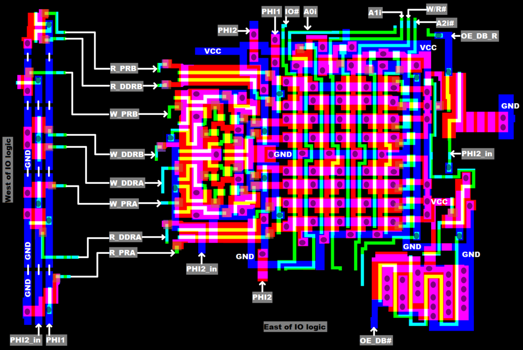
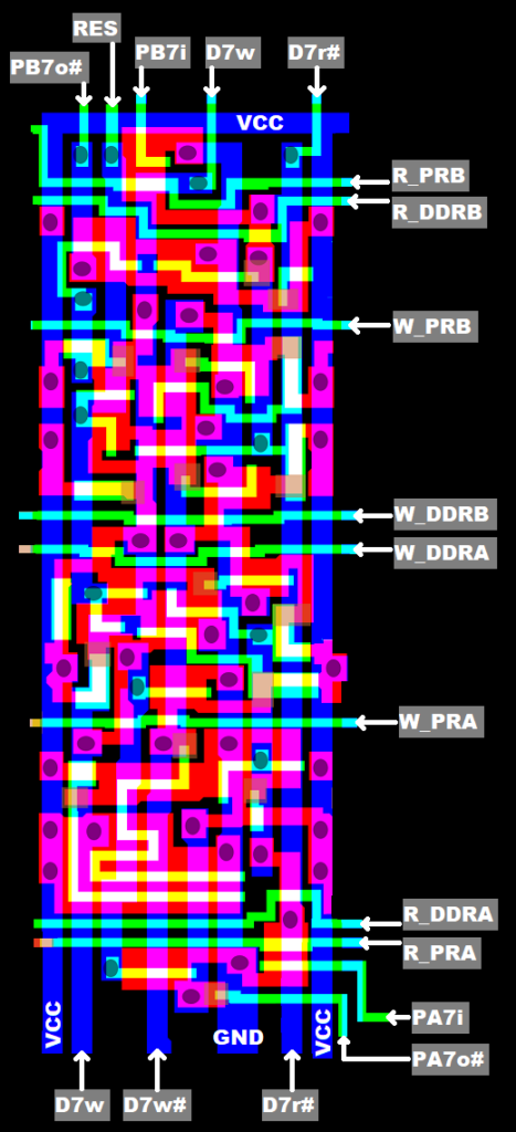
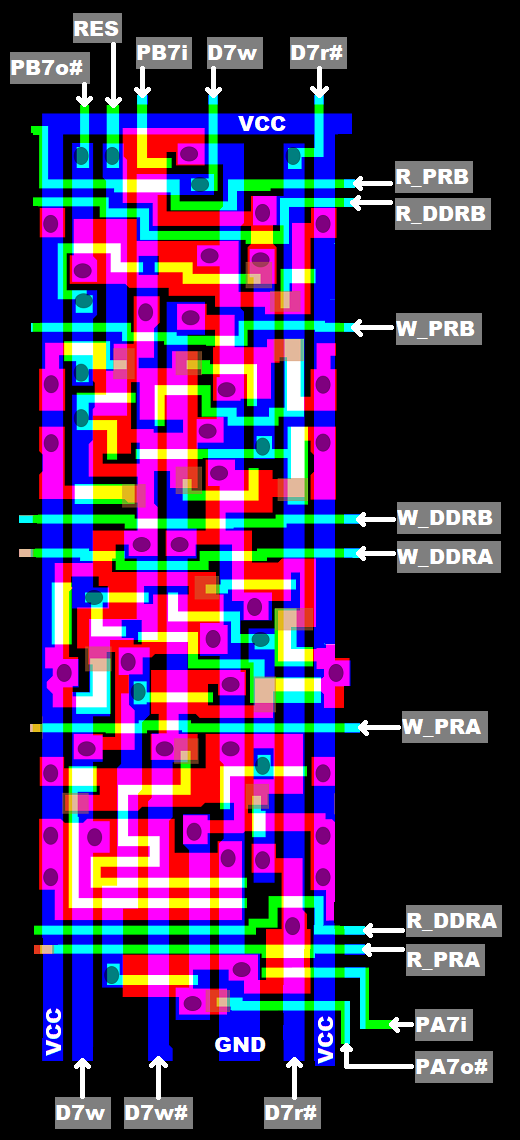
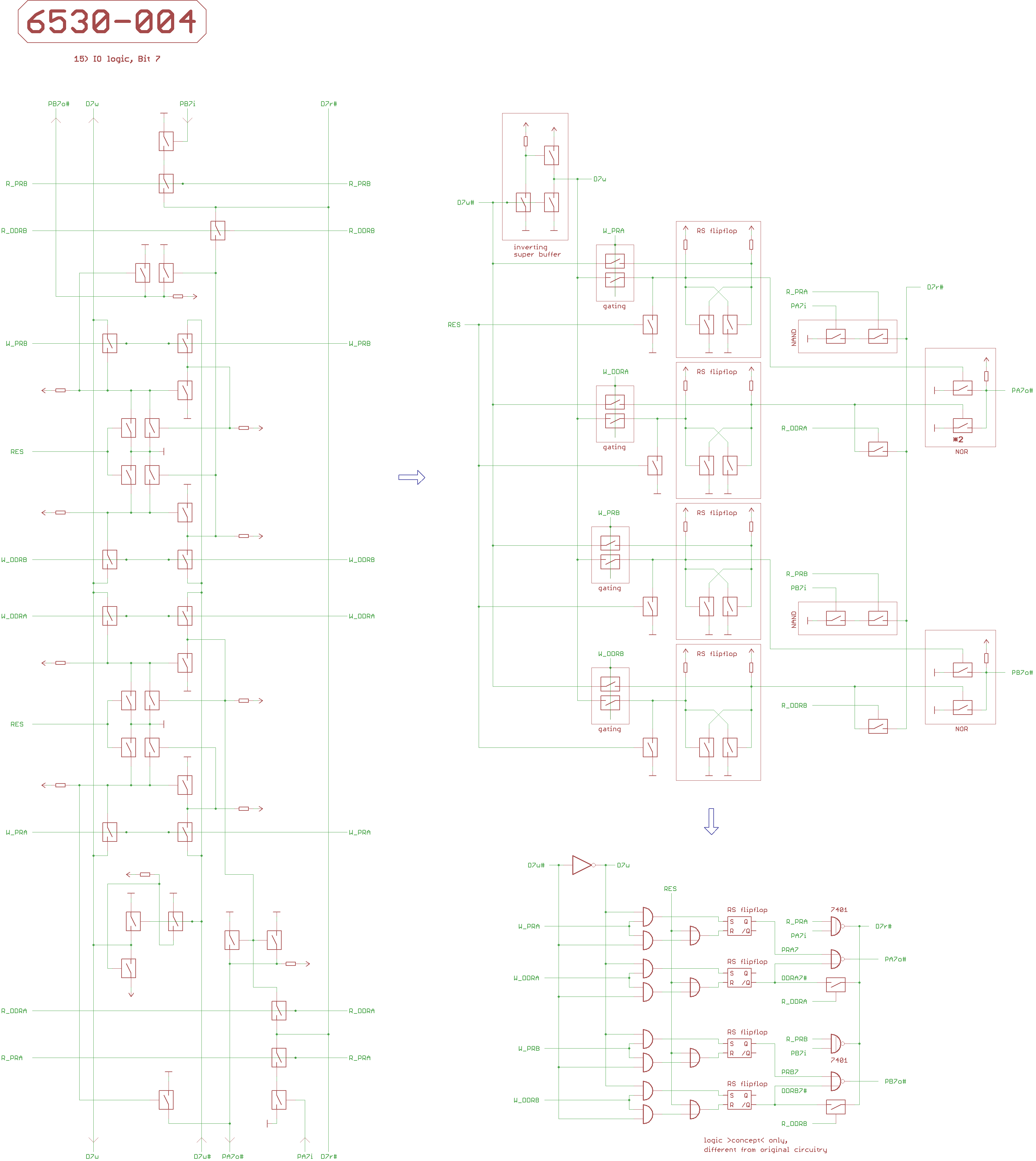
15 IO logic
IO logic block is located East of the PB0, PB1 buffers/drivers and West of the IO control block.
South in the IO logic block, we have eight inverting super buffers, which generate D0..7w (high_active) from D0..7w# (low-active).
Since the layout for the IO block Bits is more or less identical, we just focus on the IO logic for Bit 7.
Output side:
PRA (write) is data register for port A output (PA0..7).
DDRA (write) is data direction register for port A, if a Bit is 1 this means the according PA0..7 pin is configurated to work as an output.
The PRA, DDRA register Bits are static RS flipflops, which are cleared during RES=high.
Note, that RES (high_active) is the inverted signal from the RES# pad (low-active), not sampled by any clock, take care.
When one of the IO the write control signals W_PRA, W_DDRA, goes high, D0..7w and D0..7w# are fed to both transistors of a RS flipflop in the according register Bit by FET switches.
And yes, that’s “differential” signals and two FET switches per register Bit.
For PA1..7, we have seven NOR gates which generate PA1..7o# signals, telling the output drivers to pull PA1..7 to GND,
when a PRA register Bit is 0 and the according DDRA register Bit is 1 (when PA1..7 is configurated as an output).
//pull-up resistors (FETs) to VCC are pulling PA1..7 to high when the output drivers are not pulling PA1..7 to GND.
Since the PA0 output is a true push/pull driver, it lacks the NOR gate.
See “11) PB0”, which discusses the PA0 and PB0 driver/buffer circuitry.
For port B, the game is similar, just with PB0..7, PRB and DDRB.
But in the chip we had dissected, the PB5 and PB6 drivers were disabled because PB5 and PB6 were used as inputs for chip select signals.
Also, PB7 can be used as #IRQ output, and in this case the Timer control block overrides PRB and DDRB when generating an interrupt on PB7.
Note, that PB7 lacks the pull-up resistor (FET), means one has to add an external pull-up resistor for a logic high level on PB7.
Input side:
When reading DDRA, the DDRA register Bits are placed on the read data bus D0..7r# in inverted form by FET switches, and that’s all there is to it.
The signals from the PA1..7 pads are buffered as PA1..7i.
When reading PRA0..7, we have eight “open collector” NAND gates which pull the read data bus D0..7r# low
if the according DDRA Bit is low (PA1..7 configurated as an input, that is) and PA0..7i is high.
For PA0i it’s a bit different:
If PA0 is configurated as an input, PA0i comes from the PA0 pad.
If PA0 is configurated as an output, PA0i comes from the PRA0 register Bit.
For details, again please see “11) PB0”, which discusses the PA0 and PB0 driver/buffer circuitry.
For Port B, the game is similar.
65xx peripheral chips usually sample port input signals during PHI1, but the 6530 doesn’t.
6530 just places the signals from the IO port on the DB0..7 CPU data bus, the 6502 samples DB0..7 at the falling edge of PHI2, and that’s it.
That’s not good for signal integrity.
[i]See, many years ago I had built counters for incremental encoders at work with XC95108 CPLD chips.
Out of paranoia, I had tied three counters to one encoder, and after some hours of operation all of them counters had a different value.
For position control in machine engineering, that’s not good.
I had tried a lot of different things:
– creative placement of capacitors of different size into the power supply, active/passive termination of the clock signal,
– filtering the signal inputs with shift registers and whatnot…
What eventually had fixed the problem was running the counter with the non_inverted clock,
and putting flipflops controlled by the inverted clock into the input signals.
Sounds familiar when talking about PHI1 and PHI2… but I’m getting off topic.[/i]
Whether you want to have transparent latches sampling PA0..7 and PB0..7 during PHI1 or not
when building a TTL or FPGA implementation of the 6530, that’s your decision.

16 Timer control
The Timer control block is located North of the DB3, DB4 drivers/buffers, East from the Timer block.
Also, we have a little bit of logic for Timer Interrupt flag and PB7 IRQ generation West from the Timer block,
which technically also belongs to the Timer control block.
Address decoding:
To make things simple:
We have three NOR gates, which generate three high_active control signals when PHI1 is low
(what is different from “PHI2 is high”) AND when IO is selected AND when A2i is high.
R_TMR (read Timer) when A0i is low AND W/R# is low (read).
R_IRQ (read Timer underflow Interrupt flag) when A0i is high AND W/R# is low (read).
W_TMR (write timer) when W/R# is high (write). //Note: A0i doesn’t matter here.
R_TMR and W_TMR are switched to GND by FETs during PHI1:
For R_TMR, one FET located West from the Timer block.
For W_TMR, one FET located West from the Timer block, and another FET located in pre-scaler counter Bit 0.
Predivider control:
We have a predivider, basically a ten Bit down counter running at PHI2_in speed,
which is cleared when writing the Timer by W_TMR.
//Predivider counter Bits change with PHI2.
We have three latches for the pre-scaler factor, written with W_TMR.
Depending on A0i and A1i, only one of the latches can be set to 1, default is 0.
00: PRE1=1, PRE8=0, PRE64=0. No predivider, Timer is running at PHI2_in speed.
01: PRE1=0, PRE8=1, PRE64=0. Predivider factor 8, Timer is running at PHI2_in/8.
10: PRE1=0, PRE8=0, PRE64=1. Predivider factor 64, Timer is running at PHI2_in/64.
11: PRE1=0, PRE8=0, PRE64=0. Predivider factor 1024, Timer is running at PHI2_in/1024.
Active predivider counter Bits:
Three when PRE8=1.
Six when PRE64=1.
Else, all of the ten predivider Bits are active.
In the predivider block, we have a ten input NOR gate which generates the IS0 signal.
If IS0 is high, all of the active predivider counter Bits are zero. //I’m simplifying things a bit here.
Timer control:
We have a Timer, basically an eight Bit down counter,
read with R_TMR, written with W_TMR,
Timer Bits change with PHI2.
The low-active CEN# signal enables Timer counting.
If PRE1 is high, CEN# always is active, and the Timer is running at PHI2_in speed.
;
IS0 is sampled with a transparent latch at PHI1,
means that if IS0 was high in the previous PHI2_in cycle, CEN# is active for the current PHI2_in cycle.
;
If the Interrupt flag is set, CEN# is active: the timer is running at full speed.
;
W_TMR also puts CEN# active, and I don’t know why,
because the Timer counter circuity ignores CEN# when W_TMR is active.
The Timer uses a carry lookahead mechanism for the lower 5 Bits,
that’s why we have that Tcin5 signal, we are getting there later in “18) Timer”.
Timer underflow Interrupt flag and IRQ generation:
6530 Interrupt flag basically is a RS flipflop built from two NOR gates.
Timer Bit 7 carry output TC# (low-active, signaling Timer underflow, changes with PHI2) is sampled with a transparent latch during PHI1.
TC# is active, when the (decrementing) Timer is at $00 in the current PHI2_in cycle (and will roll over to $FF in the next time).
If TC# was active in the previous PHI2_in cycle, the latch output does set the 6530 Interrupt flag (through an inverter)
during PHI1 in the current PHI2_in cycle.
We have another transparent latch, which samples the Interrupt flag during PHI2.
If the output of that latch is active, three things will happen:
;
CEN# is active, the Timer counts a step during the current PHI2_in cycle.
;
If the PB7 IRQ output is not disabled, AND RESET is not active,
the IRQ signal goes active during PHI2 of the current PHI2_cycle and tells the PB7 driver to pull PB7 to GND.
//If PB7 is tied to the IRQ# input of the 6502, this signals a 6530 Timer underflow IRQ# to the 6502.
;
When the Interrupt flag is read by R_IRQ during PHI2, read data bus D7r# is pulled low,
means the 6502 sees DB7 ‘1’ what indicates that the 6530 Interrupt flag is set.
//read data bus D0..7r# lines which are not pulled to GND during PHI2 give us ‘0’ on DB0..7.
//That’s why DB0..6 are ‘0’ when reading the Interrupt flag.
The Interrupt flag is cleared in the current PHI2_in cycle by reading/writing the Timer (if R_TMR OR W_TMR goes high).
Now for the last part: disabling PB7 IRQ.
We have a latch which samples A3i# during Timer reads (R_TMR=high) OR Timer writes (W_TMR=high).
The output of that latch gives us the signal IRQ_DISABLE.
If IRQ_DISABLE is high, IRQ is disabled, and the Timer Interrupt flag won’t cause that PB7 is pulled low.
When reading/writing the Timer,
A3i=0 disables and A3i=1 enables PB7 IRQ generation during PHI2 in the current PHI2_in cycle.
Also, the Interrupt flag is cleared in the current PHI2_in cycle.
Note, that the PB7 IRQ generation ignores the PRB7 and DDRB7 IO register Bits.
Also note, that RESET does not affect the 6530 Interrupt flag, Timer, pre-scaler, and pre-scaler factor.
RES makes sure that PB7 is not pulled low by IRQ while RES is active.
RES also sets the latch for the PB7 interrupt generation to “disabled”.
But if there is something like an accidental Timer read during the RESET sequence of a 6502,
A3i could enable PB7 interrupt generation, and then there might be a falling edge on PB7 in the wrong moment…
If PB7 is tied to IRQ# of the 6502, there is no problem, because the 6502 does not mind an active IRQ# during its RESET sequence.
If PB7 is tied to NMI# of the 6502, there is a problem, because a falling edge on #NMI in the wrong time might disrupt the 6502 RESET sequence.
And that the RES# input of the 6530 is not synchronized with a clock actually makes things worse, because the 6502 _does_ synchronize its RES# input with a clock.
For more info, please read [url=http://archive.6502.org/datasheets/rockwell_r6530_r6532_timer_interrupt_precautions.pdf]Rockwell 6532 timer interrupt precautions[/url].

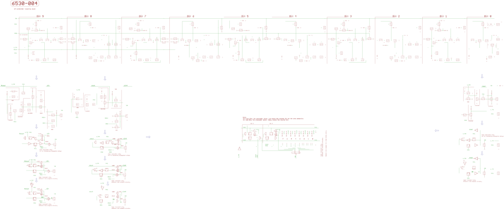
17 Predivider
The predivider is located between the ROM and the DB1, DB2 drivers/buffers,
East from the Timer control block.
Basically, it’s a 10 Bit down counter, and the carry is inverted with every Bit.
Counter Bits change with PHI2.
We have a 10 input NOR gate, it generates the IS0 signal (high_active), which indicates that the active predivider Bits are zero.
Actually, the NOR gate is just a metal trace connected to a pull-up resistor which is located in predivider Bit 0,
and there is a FET switching that metal trace to GND in every predivider counter Bit if said Bit is not zero…
…but before we are getting to the details:
The predivider breaks in three parts:
Bit 9..6 (five Bits) are controlled by PRE64 and PRE8.
Bit 5..3 (three Bits) are controlled by PRE8.
Bit 2..0 (three Bits) are free running.
If PRE64 and PRE8 are low, all of the 10 predivider counter Bits are active, what gives us a predivider factor of 1024.
If PRE64 is high, only Bit 5..0 of the predivider counter Bits are active, that’s six Bits, what gives us a predivider factor of 64.
If PRE8 is high, only Bit 2..0 of the predivider counter Bits are active, that’s three Bits, what gives us a predivider factor of 8.
However, if a predivider counter Bit is “active”, this just means that the IS0 NOR gate is sensing said counter Bit.
For even predivider counter Bits, the input of the IS0 NOR gate is just disabled, but the Bits still are able to count.
For odd predivider counter Bits, the counter Bit really is cleared.
It isn’t that bad, because when the Timer is written with W_TMR is high, all of the predivider counter Bits are cleared.
And the only way to change the pre-scaler factor (signals PRE64 and PRE8, that is) is to write the Timer.
Note: predivider counter Bit 0 contains a FET switching W_TMR to GND during PHI1, this already was mentioned in “16) Timer control”.
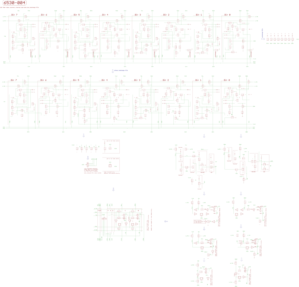
18 Timer
The Timer is located North of the DB7..5 drivers/buffers,
West from the Timer control block.
Basically, it’s an 8 Bit down counter, and the carry is inverted with every Bit.
Counter Bits change with PHI2.
It uses a carry lookahead mechanism for the lower 5 Bits, basically a six input NOR gate.
Note, that the NOR gate FET for every odd Bit is located in the next higher Bit.
Timer control block enables Timer Bit 0..5 counting with CEN# (low-active).
A dynamic transparent latch (located in the Timer control block) samples CEN# during PHI2.
If the output of that latch is low, AND if Timer Bits 0..4 are zero, the output of the six input NOR gate
Tcin5 (high_active Timer Bit 5 input carry) is high, what enables counting for Timer Bits 5..7.
The low-active TC# signal is the output carry of Timer Bit 7,
it tells the Timer control block about a Timer underflow.
//When the (decrementing) counter is $00, and wants to roll over to $FF in the next time.
If R_TMR is high, Timer contents are placed on the (low-active) read data bus D7..0r# by FET switches.
If W_TMR is high, Timer is written with the write data bus.
Even Bits are written with low-active data, odd Bits are written with high_active data, take care.
//The inverting super buffers for the write data bus which generate D0..7w from D0..7w# are South in the IO logic block,
//which is located North from the Timer. This already was mentioned in “15) IO logic”.
Note, that there are FETs West of the Timer block, which are switching R_TMR and W_TMR to GND during PHI1,
this already was mentioned in “16) Timer control”.
Dynamic pre-charge mechanism for read data bus:
There are eight pre-charge FETs South in the Timer block.
During PHI1, the FETs are active, acting as “pull-up resistors” for the read data bus D0..7r#.
Due to the bus capacitances, D0..7r# remain high during PHI2 (if PHI2_in doesn’t get too slow, that is).
During PHI2, the pre-charge FET switches are open,
and everything connected to the read data bus can pull the charge on the read bus lines to GND.
Short form:
The read data bus is low-active, and pre-charged to VCC during PHI1,
so if a read data bus line isn’t pulled to GND during PHI2, it keeps the charge.
And that’s why Bits on the read data bus default to ‘0’ on DB0..7 for the 6502.

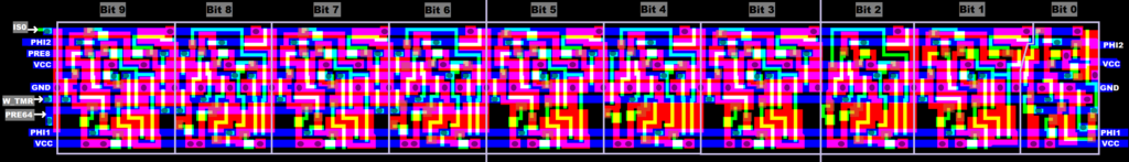
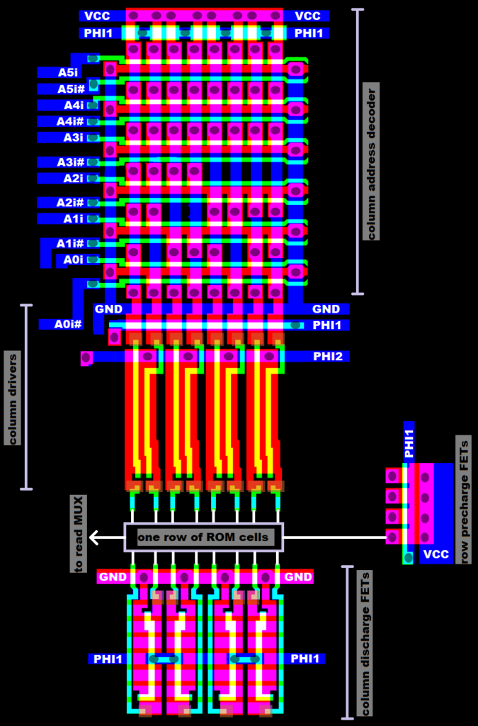
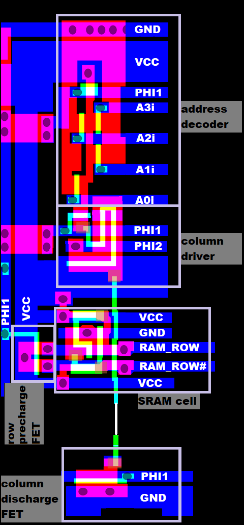
19 RAM
6530 contains 64 Bytes of static RAM.

From North to South,
we have the RAM address decoder, the column select signal drivers, then the RAM cells,
then the FETs which discharge the colum select signals by switching them to GND during PHI1.
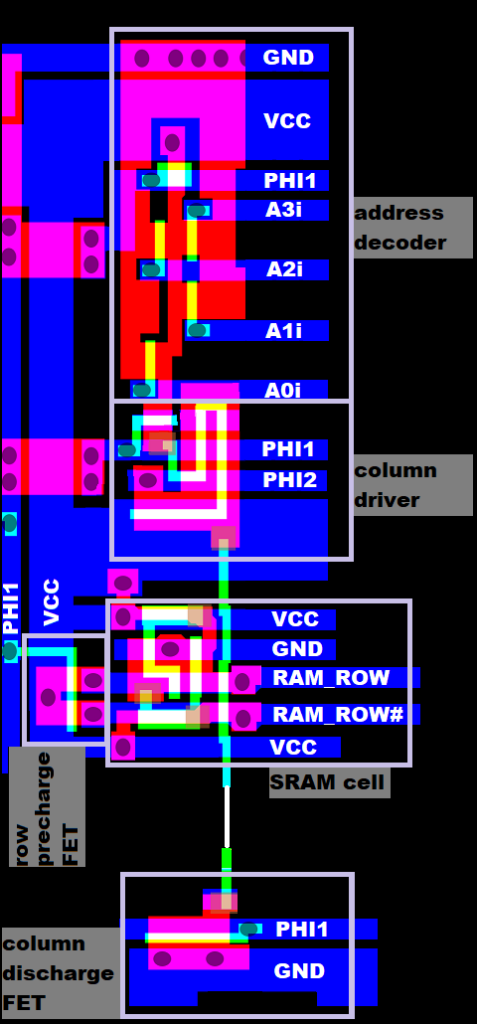
North in the RAM block, the column address decoder is fed by A0..3i (A0..3i# respectively).
It contains sixteen 4 input NOR gates.
Note, that the pull-up resistor for every NOR gate is not tied to VCC directly/permanently, but only during PHI1.
To be more precise, we have FET switches controlled by PHI1, and the impedance of a FET is working as a resistor.
//From West to East, the NOR gates check from 0000 to 1111, it’s linear.
South from the column address decoder, we have the column select signal drivers:
Sixteen transparent latches, sampling the outputs of said NOR gates during PHI2,
control sixteen FET switches, which connect one of the sixteen column select signals to PHI2.
Means, only one column select signal is active at a time.
At the Southern corner of the RAM block, we have FETs switching all of the column select lines to GND during PHI1.
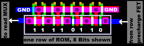
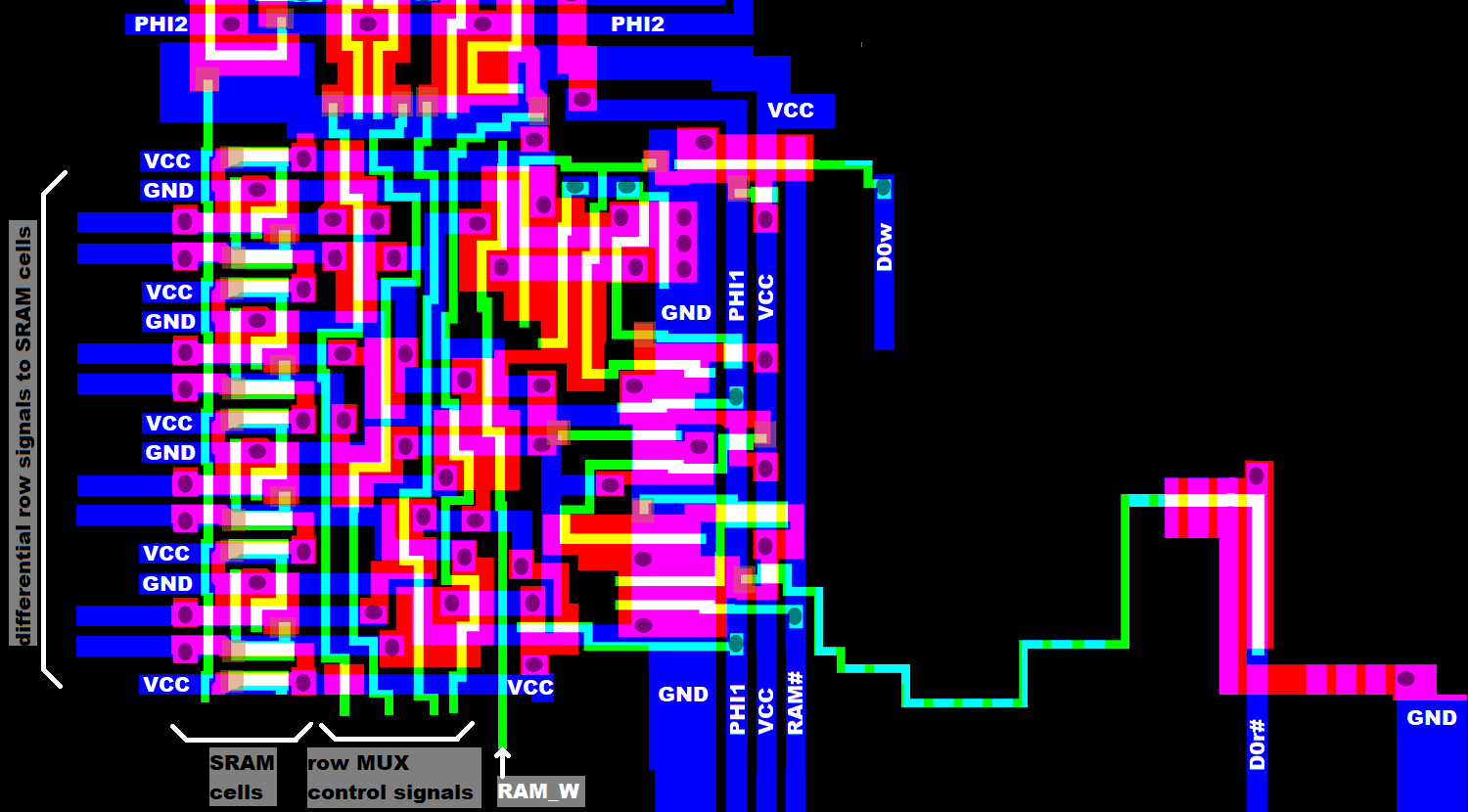
RAM cells are organized in eight parts, for D0..D7,
starting with D0 South of the column select signal drivers, followed by D1, and so on.
In each of the eight D0..D7 RAM cell areas, we have RAM cells arranged in a “4 rows and 16 columns” pattern.
//That’s 64 RAM cells in total for every Bit on the data bus.
Each RAM cell contains a conventional RS flipflop (built from two FETs and two pull-up resistors (FETs)),
plus two FET switches (controlled by the column select signals) connecting the RS flipflop to the row signals
RAM_ROW and RAM_ROW# during PHI2.
At the Western corner of the RAM block, we have pre-charge FETs switching the RAM_ROW and RAM_ROW# signals
for every line of RAM cells to VCC during PHI1, switches have an impedance which makes them act like pull-up resistors.
//That’s 8*4*2 = 64 pre-charge FETs in total for 64 Bytes of RAM.
RAM cells are read/written only during PHI2.
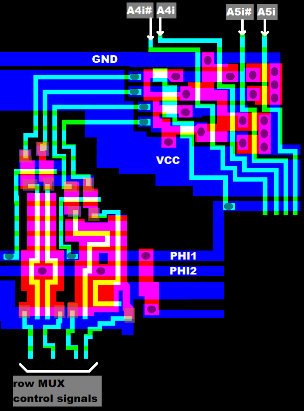
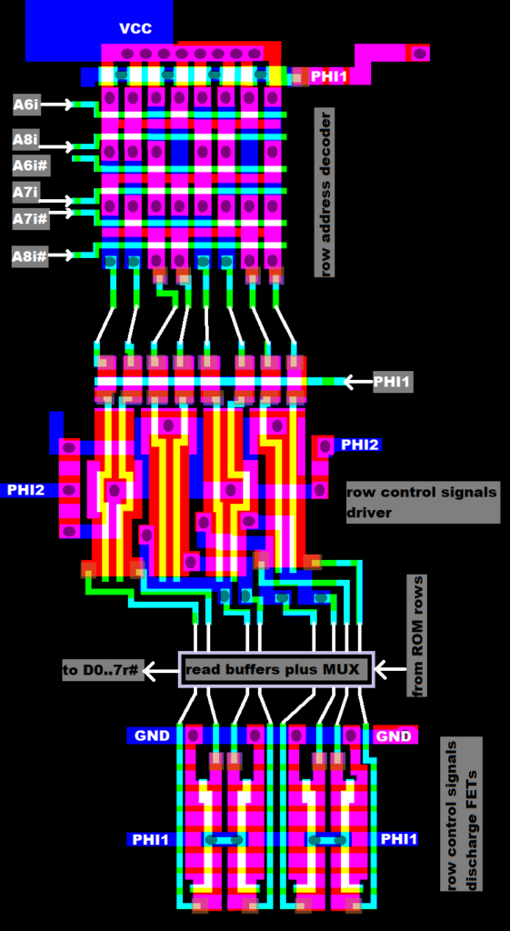
East of the column decoder plus drivers, we have the row decoders plus drivers,
and except that they are fed with A5i and A6i (A5i# and A6i# respectively),
conceptually they are not much different from the column decoders plus drivers.
They control 4:1 multiplexers East of the RAM cells.
For every Bit on the data bus, we have two 4:1 multiplexers,
one connecting the RAM_ROW signals from four rows of RAM cells to the read/write driver/buffer of a data Bit,
the other connecting the RAM_ROW# signals from four rows of RAM cells to the read/write driver/buffer of a data Bit.
//One row has 16 RAM cells.
Note, that the multiplexers are just FET switches, and that signals can go through said switches in both directions.
To be more precise:
When reading RAM cells, signals from the RAM cells to the read buffers go through the multiplexers from West to East.
When writing RAM cells, signals from the write drivers to the RAM cells go through the multiplexers from East to West.
According to A5i and A6i, the multiplexers are selecting the rows in the pattern:
00
01
11
10
But since all of the RAM cells are identical, we can safely ignore this.

Now for the read/write drivers/buffers.
West of the multiplexers we have the RAM cells, East of the multiplexers we have the read/write drivers/buffers.
At the read/write driver/buffer side of the multiplexers, we have two FETs,
precharging RAM_ROW and RAM_ROW# of said read/write drivers/buffers to high during PHI1.
On the write side, we just have a “differential” push/pull line driver, fed by a Bit on the write data bus D0..7w (high_active).
The driver outputs are enabled when RAM_W is high, during PHI1=0 (what is different from “PHI2=1”),
setting the RAM_ROW and RAM_ROW# signals of the selected row of RAM cells through the two 4:1 multiplexers.
;
PHI1 and PHI2 are not overlapping, the line driver outputs are enabled during PHI1=0,
so that RAM_ROW and RAM_ROW# at the RAM cells are valid before the rising edge of PHI2.
//The RAM cells connect to RAM_ROW and RAM_ROW# during PHI2.
On the read side, we have a RS flipflop which is brought into a controlled state during PHI1,
and flipped (or not flipped) by the RAM_ROW# signals from the RAM cells during PHI2.
;
The side of the RS flipflop which is switched to GND during PHI1 goes through an inverter,
then into a two input NOR gate together with RAM# (low-active RAM enable signal which changes during PHI1).
The output of that NOR gate drives a FET which pulls a Bit on the read data bus to GND, and that’s all.
;
To be more precise:
The output FET can’t pull a Bit on the read data bus to GND during PHI1,
because the side of the RS flipflop that goes through an inverter into the NOR gate controlling the output FET
is switched to GND during PHI1.
20 ROM
6530 contains 1024 Bytes of mask programmed NOR ROM.
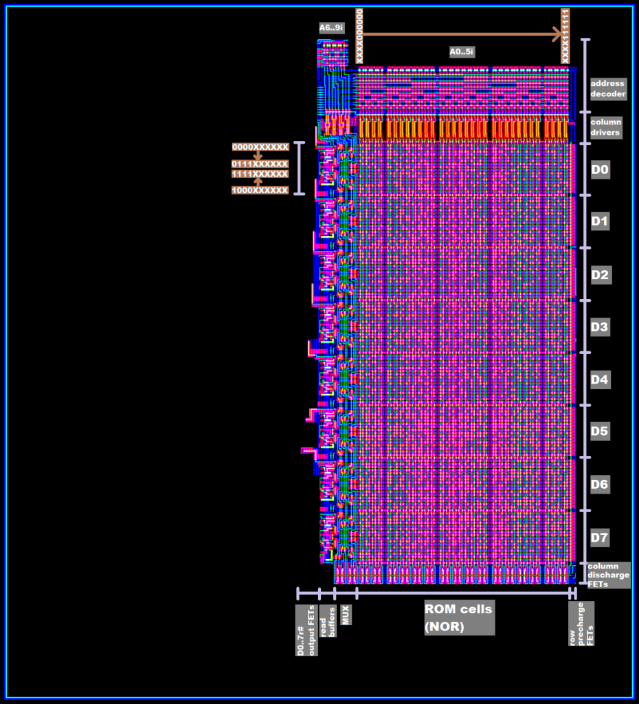
From North to South,
we have the ROM address decoder, the column select signal drivers, then the ROM cells,
then the FETs which discharge the colum select signals by switching them to GND during PHI1.
North in the ROM block, the column address decoder is fed by A0..5i (A0..5i# respectively).
It’s a PLA like structure of 64 six input NOR gates.
Note, that the pull-up resistor for every NOR gate is not tied to VCC directly, but only during PHI1.
To be more precise, we have FET switches controlled by PHI1, and the impedance of the FETs is working as a resistor.
//From West to East, the NOR gates check from 000000 to 111111, it’s linear.
South from the column address decoder, we have the column control signal drivers:
64 transparent latches, sampling the outputs of said NOR gates during PHI2,
control 64 FET switches, which connect one of the sixteen column select signals to PHI2.
Means, only one column select signal is active at a time.
At the Southern corner of the ROM block, we have FETs switching all of the column select lines to GND during PHI1.
//The game isn’t much different from what we had in the RAM block so far.
ROM cells are organized in eight parts, for D0..D7,
starting with D0 South of the column control signal drivers, followed by D1, and so on.
In each of the eight D0..D7 ROM cell areas, we have 16 mask programmed NOR gates, one gate per row,
with up to 64 inputs each (which connect to the high_active column select signals).
Mask programmed means, that an input transistor of the NOR gate connecting to one of the 64 column select signals
is present or missing.
Mask programming was done by changes in the diffusion layer, like in “12) PLA”.
If the transistor in a NOR gate connecting to a column select signal is present,
said NOR gate emits 0 when the column select signal goes active (high) during PHI2.
Transistor present: Data Bit is 1.
Transistor missing: Data Bit is 0.
Like in the column address decoder, the (up to) 64 input NOR gates don’t have a pull-up resistor
which is tied to VCC directly/permanently, but only during PHI1.
To be more precise, we have 8*16 = 64 FET switches controlled by PHI1,
the row pre-charge FETs, and the impedance of the FETs is working as a resistor.
If you take a closer look at the PLA like structure of the column address decoder,
and rotate it by 90 degrees clockwise, it looks pretty much like the ROM cells, doesn’t it ?
East of the column decoder plus drivers, we have the row decoders plus drivers,
and except that they are fed with A6..8i (A6..8i# respectively),
conceptually they are not much different from the column decoders plus drivers.
They control two 8:1 multiplexers West of the ROM NOR gates per Data Bit.
Each of the 8:1 multiplexer inputs is fed by the outputs of 8 ROM NOR gates.
The outputs of the two multiplexers go into another 2:1 multiplexer controlled by A9i (and A9i# respectively),
which then gives the signal to a read buffer for every Bit on the data bus.
Note:
The multiplexer for the second 8 rows of NOR gates has the inputs in reversed order.
From North to south, the selection of ROM NOR gates according to A6..9i actually is:
0000 up to 0111, and then 1111 down to 1000.
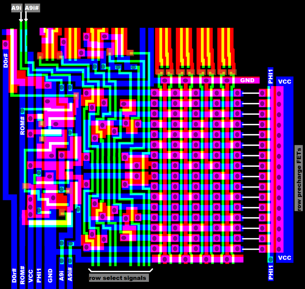
Now for the ROM read buffers.
The game is very similar to the read buffers in the RAM.
Outputs of the two 8:1 multiplexer and the 2:1 multiplexer are pre-charged by FET switches
(with some impedance to make them work as pull-up resistors) during PHI1.
Again, we have a RS flipflop which is brought into a controlled state during PHI1,
and flipped (or not flipped) by the output of the 2:1 multiplexer during PHI2.
;
The side of the RS flipflop which is switched to GND during PHI1 goes through an inverter,
then into a two input NOR gate together with ROM# (low-active ROM enable signal which changes during PHI1).
The output of that NOR gate drives a FET which pulls a Bit on the read data bus to GND, and that’s all.
;
To be more precise:
The output FET can’t pull a Bit on the read data bus to GND during PHI1,
because the side of the RS flipflop that goes through an inverter into the NOR gate controlling the output FET
is switched to GND during PHI1.
Just one more word about the output FETs of the RAM and the ROM, switching the read data bus to GND.
It’s an incredibly compact design, and for most of the Bits on the read data bus,
the output FETs of the RAM and the ROM are close together, forming a big NOR gate.
Letter from Bill Mensch on the creation of the 6530
Bill Mensch wrote:
I would be happy to contribute some commentary concerning the creation of the 6530 at MOS.
What are you interested in other than it was the second chip for the combination of the 6502 for use in control systems.
The KIM-1 was a reference design/use case for bothe the 6502 and the 6530, actually two of them.
One 6530 was for the “Teletype Input Monitor (TIM)” and the other one was for the “Keypad Input Monitor (KIM)”.
It was first demonstrated along with the 6501/6502 at the WESCON ’75.
The 6502 and 6530 were ment to compete with the $29 Intel 4040 two chip controller combo.
The actual design was important for the introduction of the 6502.
I and a team of three mask designers Harry Bawcom, Mike Jaynes and Sid Holdt created the 6530.
The timer design was patented and used on the 6530, 6531 and 6532 chips.
Chuck Peddle and Wil Mathys contributed the system level applications concepts and requested the features.
We were a small team. I was the semiconductor design and architect engineer.
The 6530 followed many of the design concepts of the 6820/6520/6821/6520 concepts for IO and interrupt features.
The 6522 followed the 6520/6530/6532 designs at MOS.
Ray Hirt was the project lead on the 6532.
The 6532 RIOT design was basically to remove the ROM and add another 64 bytes of RAM for a total of 128 bytes.
I was the microprocessor design manager at this time replacing Rod Orgill who had left MOS to work at NCR in Colorado Springs, CO.
Rod didn’t work on any of the IO chips, just the 6501/6502.
Ray, Rod, sometimes Wil and I shared many a pitcher of beer at many lunches after the 6502 and 6530/32 were completed before Rod left for Colorado.
These are fond memories of my time at MOS.
Let me know if you have any questions.
Best,
-Bill


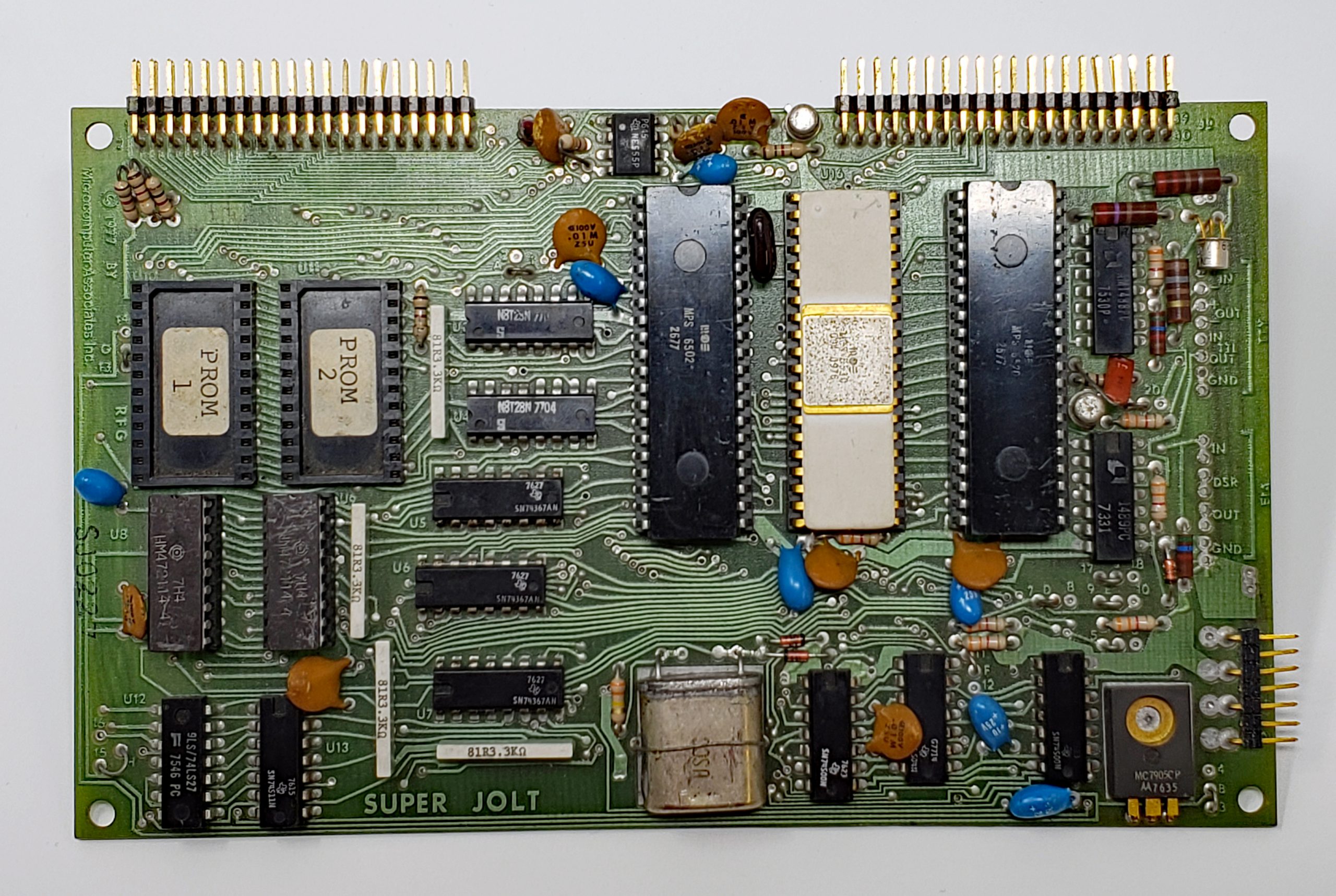
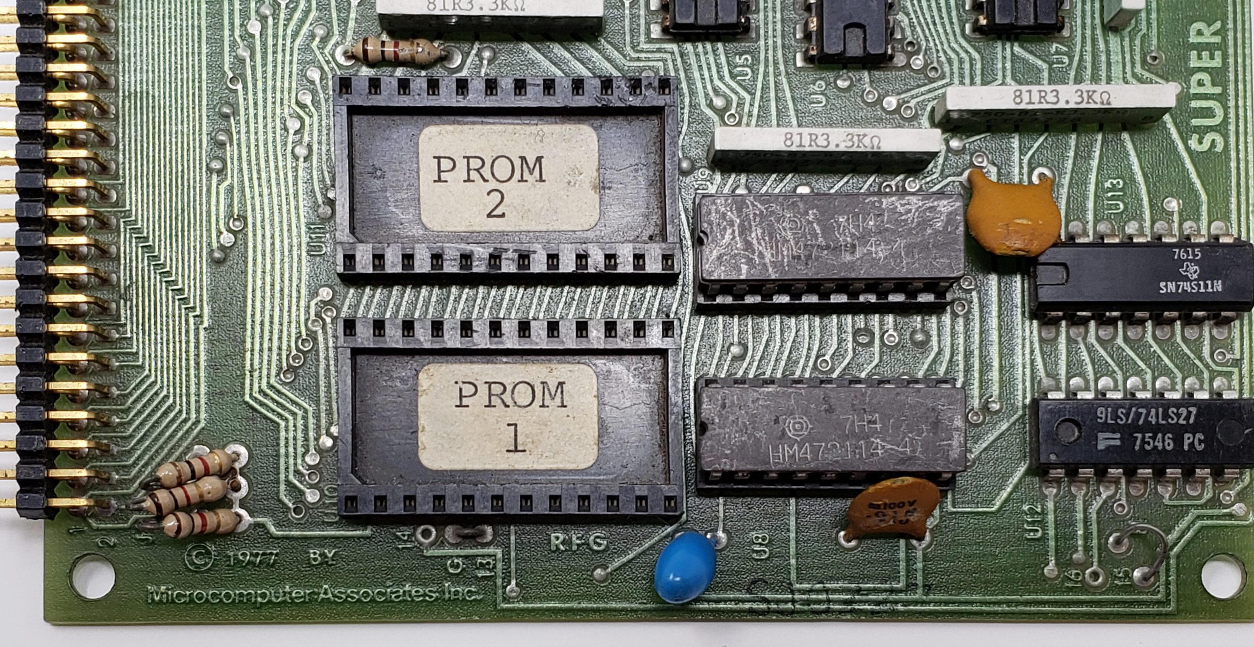
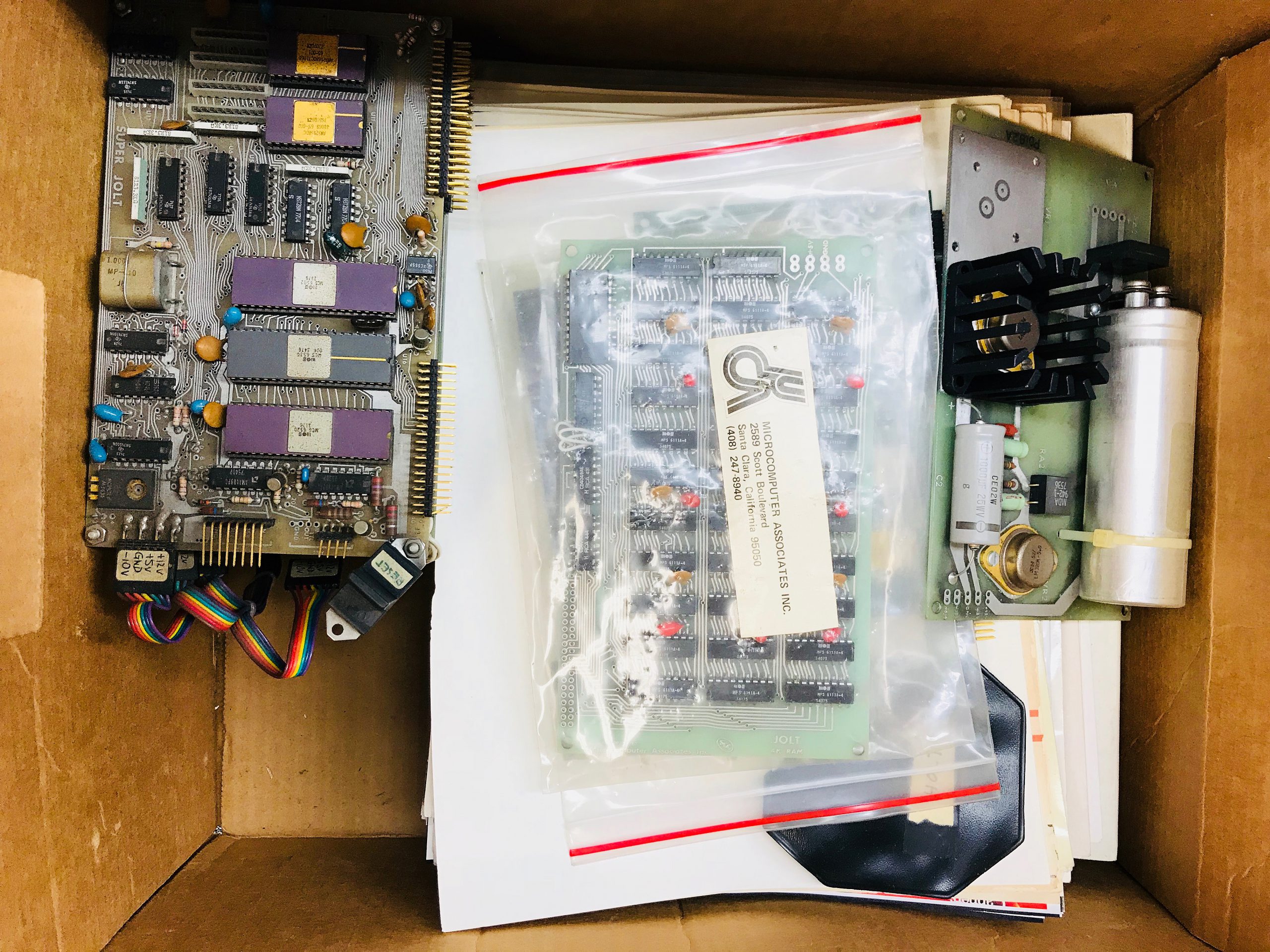


 Read here for the circuit diagram and assembler source.