
I2C Bus interface
Hardware
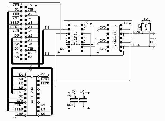
The connector on the top left of the diagram is from my own 6502 boards (see the sbc project) and is as it is for two reasons. It’s easy to wire on a stripboard layout and I have a lot of 26 way ribbon, headers and plugs. All the signals are directly from the 6502 except /SEL0 and /SEL1 which are used to select the block $F1xx with /SEL0 = 1 and /SEL1 = 0.
There is no socket shown for the I2C bus, this is up to the user.The two capacitors are low ESR electrolytics and are placed near the GAL and between the two chips. If you don’t have this type to hand you can use standard electrolytics with some low value ceramic capacitor, say 0.1uF, in parallel.
The GAL16V8A is used purely to generate the read and write strobes. Each is a negative going pulse coincident with phase 2. The interface uses just one byte in the address range. For anyone interested the equations for this chip are in i2c_01.pld and can be compiled with WinCUPL. The fuse file, i2c_01.jed and the compiler list file i2c_01.txt are also included.
The 74LS74 is used to latch the two lowest bits of the data bus during write access to the interface. The reset line is connected so that both of these outputs are set at startup (this disables the I2C bus until required). This is very similar to my AT keyboard with the exeption that reset sets the opposite state.
The outputs from the latches are used to drive the enable pins on two of the four buffers from the 74LS125, these are then used to drive the data and clock lines of the I2C bus. The buffers have their inputs tied low so behave like open collector outputs when used like this. The other two buffers are used to drive the data bus during read access.
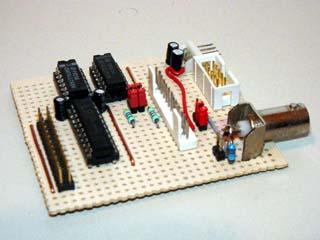
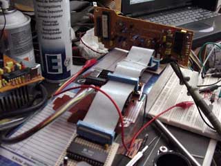
The finished board
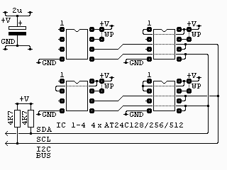
256k byte memory
Software
The software has a four main routines to handle the I2C bus
| SendAddr | Send start and slave address to the I2C bus. |
| SendData | Send data byte(s) to an addressed device. |
| ReadData | Read data byte(s) from an addressed device. |
| StopI2c | generates a stop condition on the i2c bus. |
This is a description of all the I2C routines
SendAddr
This routine sends the slave address to the I2C bus. There are a number of locations that need set-up before this routine is called. Each device has an 8 bit address, the lowest bit of which is a read/write bit, this address is set in I2cAddr. Next is the byte count, if you are just addressing the device this can be zero but otherwise it is the byte pair in I2cCountL/H. Lastly, if there is data to be sent, is the buffer pointer TxBuffL/H. This should be set to the start of the data to be sent. If all is well this routine exits with Cb=0 and the bus in an held state, you can then either send data, receive data or just send stop.
ReadData
This routine reads I2cCountL/H bytes from an already addressed device. It should be entered with RxBuffL/H pointing to a suitable buffer area. On exit Cb=0 if there were no errors and the I2C bus is in a held state, you can then either receive more data or just send stop.
SendData
The same as ReadData but sends I2cCountL/H bytes to an already addressed device. Again on exit Cb=0 if there were no errors and the I2C bus is in a held state, you can then either send more data or just send stop.
StopI2c
This routine just generates a stop condition on i2c bus. On entry it is assumed only that the clock is held low.
ByteIn
Read a byte from the I2C bus, the byte is returned in A. Entry to this routine should be with the bus in a held state and it exits with the bus in the same state. Note there is no timeout on this routine so it could end up waiting for ever. After this routine you should send an ack but if it’s the end of what you want you can just send stop.
ByteOut
Send a byte to the I2C bus, the byte to be sent is in A. Entry to this routine should be with the bus in a held state and it exits with the bus in the same state. Note there is no timeout on this routine so it could end up waiting for ever. Returns with the ack bit in Cb=0.
DoAck
Send ack bit, the ack bit state to send is in Cb. Entry is with the clock low, then ack needs to be set and then the clock released. The routine then waits for the clock to rise before pulling it low and then exiting.
GetAck
Get the ack bit, the received ack bit is returned in Cb. Entry is with the clock low, then the data line is released followed by the clock. Then, once the clock rises, the ack bit is read.
View the I2C driver assembler source
EHBASIC teletext driver. This is a simple page select driver for the SAA5243 + SAA5231 teletext chipset
The board in use and screen shots


;------------------------------------------------------------------------------------
;
; The following is 6502 code for an I2C driver. It acts only as master.
;
; I2C uses two bi-directional (OC) lines: clock and data. The maximum bit rate for
; slow mode is 100kbits/sec (fast mode is not supported) but with a 1.8MHz 6502 the
; best you will get is about 43kbits/sec. As the 6502, which is the master, controls
; the clock line, the processor speed should not be a problem.
;
; To work as a slave the 6502 would need extra hardware to detect the start condition,
; the stop condition and extra code to handle collisions.
; This is saved for a later project.
;
; Devices are accessed using the following four subroutines.
;
; SendAddr
;	This routine sends the slave address to the I2C bus. It can also send any
;	required register address bytes by setting them up as you would data to be sent.
;	No stop is sent so you can either read or write after calling this routine.
; SendData
;	Send data byte(s) to an addressed device. Set the count in I2cCountL/H and
;	point to the data with TxBuffL/H. No stop is sent after calling this routine.
; ReadData
;	Read data byte(s) from an addressed device. Set the count in I2cCountL/H and
;	point to the buffer with RxBuffL/H. No stop is sent after calling this routine.
; StopI2c
;	generates a stop condition on the i2c bus
;
; Each device has an 8 bit address, the lowest bit of which is a read/write bit.
;
;------------------------------------------------------------------------------------

I2CPort	=	$F121			; i2c bus port, o.c. outputs, tristate inputs
					; bit 0 is data  [SDA]
					; bit 1 is clock [SLC]
					; bits 2 to 7 are unused
RxBuffL		=	$F1		; receive buffer pointer low byte
TxBuffL		=	RxBuffL		; the same (can't do both at once!)
RxBuffH		=	$F2		; receive buffer pointer high byte
TxBuffH		=	RxBuffH		; the same (can't do both at once!)
ByteBuff	=	$F3		; byte buffer for Tx/Rx routines
I2cAddr		=	$F4		; Tx/Rx address
I2cCountL	=	$F5		; Tx/Rx byte count low byte
I2cCountH	=	$F6		; Tx/Rx byte count high byte


;------------------------------------------------------------------------------------

		*=	$2000

	JMP	SendData		; vector to send data
	JMP	ReadData		; vector to read data
	JMP	SendAddr		; vector to send slave address
	JMP	StopI2c			; vector to send stop

;------------------------------------------------------------------------------------
;
; send the slave address for an i2c device. if I2cCountL is non zero then that number
; of bytes will be sent after the address (to allow register addressing, required on
; some devices). RxBuff is a pointer, in page zero, to the transmit buffer exits with
; the clock low and Cb=0 if all ok routine entered with the i2c bus in a stopped state
; [SDA=SCL=1]

SendAddr
	LDA	I2CPort			; get i2c port state
	ORA	#$01			; release data
	STA	I2CPort			; out to i2c port
	LDA	#$03			; release clock
	STA	I2CPort			; out to i2c port

	LDA	#$01			; set for data test
WaitAD
	BIT	I2CPort			; test the clock line
	BEQ	WaitAD			; wait for the data to rise

	LDA	#$02			; set for clock test
WaitAC
	BIT	I2CPort			; test the clock line
	BEQ	WaitAC			; wait for the clock to rise

	JSR	StartI2c		; generate start condition

	LDA	I2cAddr			; get address (including read/write bit)
	JSR	ByteOut			; send address byte
	BCS	StopI2c			; branch if no ack

	LDA	I2cCountL		; get byte count
	BNE	SendData		; go send if not zero

	RTS				; else exit


;------------------------------------------------------------------------------------
;
; send data to an already addressed i2c device. I2cCountL/H is the number of bytes to
; send RxBuff is a pointer, in page zero, to the transmit buffer exits with Cb=0 if
; all ok. it is assumed at least one byte is to be sent routine entered with the i2c
; bus in a held state [SCL=0]

SendData
	INC	I2cCountH		; increment count high byte
	LDY	#$00			; set index to zero
WriteLoop
	LDA	(RxBuffL),Y		; get byte from buffer
	JSR	ByteOut			; send byte to device
	BCS	StopI2c			; branch if no ack

	INY				; increment index
	BNE	NoHiWrInc		; branch if no rollover

	INC	RxBuffH			; else increment pointer high byte
NoHiWrInc
	DEC	I2cCountL		; decrement count low byte
	BNE	WriteLoop		; loop if not all done

	DEC	I2cCountH		; increment count high byte
	BNE	WriteLoop		; loop if not all done

	RET

;------------------------------------------------------------------------------------
;
; get data from already addressed i2c device. I2cCountL/H is the number of bytes to
; get, RxBuff is a pointer, in page zero, to the receive buffer. exits with Cb = 0 if
; all ok it is assumed at least one byte is to be received. the routine is entered
; with the i2c bus in a held state [SCL=0]

ReadData
	LDY	#$00			; set index to zero
ReadLoop
	DEC	I2cCountL		; decrement count low byte
	JSR	ByteIn			; get byte from device

	LDA	I2cCountL		; get count low byte
	CMP	#$01			; compare with end count + 1
	LDA	I2cCountH		; get count high byte
	SBC	#$00			; subtract carry, leaves Cb = 0 for last byte
	JSR	DoAck			; send ack bit

	LDA	ByteBuff		; get byte from byte buffer
	STA	(TxBuffL),Y		; save in device buffer
	INY				; increment index
	BNE	NoHiRdInc		; branch if no rollover

	INC	TxBuffH			; else increment pointer high byte
NoHiRdInc
	LDA	I2cCountL		; get count low byte
	BNE	ReadLoop		; loop if not all done

	DEC	I2cCountH		; decrement count high byte
	LDA	I2cCountH		; get count high byte
	CMP	#$FF			; compare with end count
	BNE	ReadLoop		; loop if not all done

	RTS


;------------------------------------------------------------------------------------
;
; generate stop condition on i2c bus. it is assumed only that the clock is low on
; entry to this routine.

StopI2c
	LDA	#$00			; now hold the data down
	STA	I2CPort			; out to i2c port

;	NOP				; need this if running > 1.9MHz
	LDA	#$02			; release the clock
	STA	I2CPort			; out to i2c port

;	NOP				; need this if running > 1.9MHz
	LDA	#$03			; now release the data (stop)
	STA	I2CPort			; out to i2c port
	RTS


;------------------------------------------------------------------------------------
;
; generate start condition on i2c bus. it is assumed that both clock and data are
; high on entry to this routine. note, another condition is A = $02 on entry

StartI2c
	STA	I2CPort			; out to i2c port

;	NOP				; need this if running > 1.9MHz
	LDA	#$00			; clock low, data low
	STA	I2CPort			; out to i2c port
	RTS


;------------------------------------------------------------------------------------
;
; output byte to 12c bus, byte is in A. returns Cb = 0 if ok. clock should be low
; after generating a start or a previously sent byte

; exits with clock held low

ByteOut
	STA	ByteBuff		; save byte for transmit
	LDX	#$08			; 8 bits to do
OutLoop
	LDA	#$00			; unshifted clock low
	ROL	ByteBuff		; bit into carry
	ROL	A			; get data from carry
	STA	I2CPort			; out to i2c port

;	NOP				; need this if running > 1.9MHz
	ORA	#$02			; clock line high
	STA	I2CPort			; out to i2c port

	LDA	#$02			; set for clock test
WaitT1
	BIT	I2CPort			; test the clock line
	BEQ	WaitT1			; wait for the clock to rise

	LDA	I2CPort			; get data bit
	AND	#$01			; set clock low
	STA	I2CPort			; out to i2c port

	DEX				; decrement count
	BNE	OutLoop			; branch if not all done

;------------------------------------------------------------------------------------
;
; clock is low, data needs to be released, then the clock needs to be released then
; we need to wait for the clock to rise and get the ack bit.

GetAck
	LDA	#$01			; float data
	STA	I2CPort			; out to i2c port

	LDA	#$03			; float clock, float data
	STA	I2CPort			; out to i2c port

	LDA	#$02			; set for clock test
WaitGA
	BIT	I2CPort			; test the clock line
	BEQ	WaitGA			; wait for the clock to rise

	LDA	I2CPort			; get data
	LSR	A			; data bit to Cb

	LDA	#$01			; clock low, data released
	STA	I2CPort			; out to i2c port
	RTS


;------------------------------------------------------------------------------------
;
; input byte from 12c bus, byte is returned in A. entry should be with the clock low
; after generating a start or a previously sent byte

; exits with clock held low

ByteIn
	LDX	#$08			; 8 bits to do
	LDA	#$01			; release data
	STA	I2CPort			; out to i2c port
InLoop
	LDA	#$03			; release clock
	STA	I2CPort			; out to i2c port

	LDA	#$02			; set for clock test
WaitR1
	BIT	I2CPort			; test the clock line
	BEQ	WaitR1			; wait for the clock to rise

	LDA	I2CPort			; get data
	ROR	A			; bit into carry
	ROL	ByteBuff		; bit into buffer

	LDA	#$01			; set clock low
	STA	I2CPort			; out to i2c port

	DEX				; decrement count
	BNE	InLoop			; branch if not all done

	RTS


;------------------------------------------------------------------------------------
;
; clock is low, ack needs to be set then the clock released then we wait for the
; clock to rise before pulling it low and finishing. Ack bit is in Cb

DoAck
	LDA	#$00			; unshifted clock low
	ROL	A			; get ack from carry
	STA	I2CPort			; out to i2c port

;	NOP				; need this if running > 1.9MHz
	ORA	#$02			; release clock
	STA	I2CPort			; out to i2c port

	LDA	#$02			; set for clock test
WaitTA
	BIT	I2CPort			; test the clock line
	BEQ	WaitTA			; wait for the clock to rise

	LDA	I2CPort			; get ack back
	AND	#$01			; hold clock
	STA	I2CPort			; out to i2c port

	RTS


;------------------------------------------------------------------------------------

	END
EhBASIC Teletext page viewer
This is a simple page select driver for the SAA5243 + SAA5231 teletext chipset. X is valid as a wildcard digit.
1 REM set memory size to 8192 for this program

5 REM simple teletext decoder page driver
6 REM there is no page read, output is via
7 REM teletext chip video out

10 REM set I2C interface values
20 TT = 34 : REM teletext chip 12c address
30 SB = $2000 : REM send byte
40 RB = £2003 : REM read byte (not used)
50 CL = $F5 : REM # bytes low (i2ccountL)
60 BL = $F1 : REM buffer ptr low  (rxbuffl)
70 AD = $F4 : REM device address (i2caddr)
80 BF = $4000 : REM buffer address
90 DIM TR(10) : REM register buffer

110 GOSUB 800 : REM setup chip
120 TR(8) = 0 : REM no clear display
130 TR(9) = 0 : REM set row
140 TR(10) = 0 : REM set column

150 GOSUB 838 : REM set registers 8 to 10
160 P3 = 49 : REM 1
161 P2 = 48 : REM 0
162 P1 = 48 : REM 0
170 GOSUB 370 : REM set search page

200 REM main program loop
210 DO
220 GOSUB 300 : REM select page
230 LOOP
299 END : REM never gets here

300 REM Select page

310 INPUT "Page no.";P$
320 IF LEN(P$)<>3 THEN 310
330 P$ = UCASE$(P$) : REM "x" to "X"

340 P1=ASC(RIGHT$(P$,1)) : REM 1s character ASCII value
350 P2=ASC(MID$(P$,2,1)) : REM 10s character ASCII value
360 P3=ASC(LEFT$(P$,1)) : REM 100s character ASCII value

365 REM dispaly the searched for page number
370 POKE BF,8 : REM register address
380 POKE BF+1,0 : REM set x value
390 POKE BF+3,0 : REM set y value
400 POKE BF+3,2 : REM set white
410 POKE BF+4,P3 : REM display page 100s
420 POKE BF+5,P2 : REM display page 10s
430 POKE BF+6,P1 : REM display page 1s
440 POKE AD,TT : REM set device address
450 DOKE BL,BF : REM set the buffer address
460 DOKE CL,7 : REM seven bytes to send
470 CALL SB : REM send byte(s)

475 REM set the page to search for
480 P1=P1-32 : REM calsulate page 1s (ASCII - 48 + 16)
490 P2=P2-32 : REM calculate page 10s (ASCII - 48 + 16)
500 P3=P3-24 : REM calculate page 100s (ASCII - 48 + 24)
510 IF P1=56 THEN P1 = 0 : REM allow wildcard "X"
520 IF P2=56 THEN P2 = 0 : REM allow wildcard "X"
530 IF P3=64 THEN P3 = 8 : REM allow wildcard "X"
540 POKE BF,2 : REM register address
550 POKE BF+1,0
560 POKE BF+2,P3
570 POKE BF+3,P2
580 POKE BF+4,P1
590 POKE AD,TT : REM set device address
600 DOKE BL,BF : REM set the buffer address
610 DOKE CL,5 : REM five bytes to send
620 CALL SB : REM send byte(s)
630 RETURN

799 END

800 REM setup teletext registers

801 RESTORE 910
802 FOR X = 1 TO 5
804 READ TR(X)
806 POKE BF+X,TR(X)
808 NEXT
810 POKE BF,1 : REM register address
812 POKE AD,TT : REM set device address
814 DOKE BL,BF : REM set the buffer address
816 DOKE CL,6 : REM six bytes to send
818 CALL SB : REM send byte

819 RESTORE 935
820 FOR X = 4 TO 7
822 READ TR(X)
824 POKE BF-3+X,TR(X)
826 NEXT
828 POKE BF,4 : REM register address
830 POKE AD,TT : REM set device address
832 DOKE BL,BF : REM set the buffer address
834 DOKE CL,5 : REM five bytes to send
836 CALL SB : REM send byte

838 RESTORE 980
839 FOR X = 8 TO 10
840 READ TR(X)
842 POKE BF-7+X,TR(X)
844 NEXT
846 POKE BF,8 : REM register address
848 POKE AD,TT : REM set device address
850 DOKE BL,BF : REM set the buffer address
852 DOKE CL,4 : REM four bytes to send
854 CALL SB : REM send byte

856 RETURN

900 REM default values for registers 1 - 3
910 DATA 4
920 DATA 0
930 DATA 25,16,16

935 REM default values for registers 4 - 7
940 DATA 0
950 DATA 207
960 DATA 0
970 DATA 39

975 REM default values for registers 8 - 10
980 DATA 16
985 DATA 0
990 DATA 0
[code]


<a name="i2c_jed"></a>
<b>GAL logic fuse file</B>
[code]
CUPL(WM)        4.7b  Serial# XX-xxxxxxxx
Device          g16v8as  Library DLIB-h-36-2
Created         Fri Mar 23 10:30:16 2001
Name            I2C_01
Partno          00
Revision        01
Date            19/03/01
Designer        Lee
Company
Assembly        None
Location
*QP20
*QF2194
*G0
*F0
*L00000 10101011011110110111011010010110
*L00256 10101011011110110111101010010110
*L02048 00000000001100000011000000100000
*L02112 00000000001111111111111111111111
*L02144 11111111111111111111111111111111
*L02176 111111111111111110
*C0E15
*77C0
Name     I2C_01 ;
PartNo   00 ;
Date     19/03/01 ;
Revision 01 ;
Designer Lee ;
Company   ;
Assembly None ;
Location  ;
Device   g16v8as ;

/* This GAL is the select logic for the I2C interface board	*/

/* Logic minimisations		None				*/
/* Optimisations			None				*/
/* Download				JEDEC/POF/PRG		*/
/* Doc File Options		fuse plot, equations	*/
/* Output				None				*/

/* *************** INPUT PINS *********************/

PIN	1 = A4	;				/* address bus		*/
PIN	2 = A3	;				/* address bus		*/
PIN	3 = A2	;				/* address bus		*/
PIN	4 = A0	;				/* address bus		*/
PIN	5 = A1	;				/* address bus		*/
PIN	6 = p02	;				/* CPU phase 2		*/
PIN	7 = RW	;				/* read write		*/
PIN	8 = !SEL1	;				/* block select		*/
PIN	9 = !SEL0	;				/* block select		*/
PIN	11 = A6	;				/* address bus		*/
PIN	12 = A5	;				/* address bus		*/
PIN	13 = A7	;				/* address bus		*/

/* *************** OUTPUT PINS *********************/

PIN  19 = !I2CR		;			/* I2C port read strobe		*/
PIN  18 = !I2CW		;			/* I2C port write strobe	*/
/*PIN  17 = 		;			/* 					*/
/*PIN  16 = 		;			/* 					*/
/*PIN  15 = 		;			/* 					*/
/*PIN  14 = 		;			/* 					*/

/* intermediate terms */

ADDR		= !A7 & !A6 & A5 & !A4 & !A3 & !A2 & !A1 & A0 & !SEL0 & SEL1 ;
							/* F121h (0010 0001)

/* Output terms */

I2CR	= ADDR &  RW & p02 ;			/* I2C port read strobe		*/
I2CW	= ADDR & !RW & p02 ;			/* I2C port write strobe	*/
*******************************************************************************
                                    I2C_01
*******************************************************************************

CUPL(WM)        4.7b Serial# XX-xxxxxxxx
Device          g16v8as  Library DLIB-h-36-2
Created         Fri Mar 23 10:30:16 2001
Name            I2C_01
Partno          00
Revision        01
Date            19/03/01
Designer        Lee
Company
Assembly        None
Location

===============================================================================
                            Expanded Product Terms
===============================================================================

ADDR =>
    A0 & !A1 & !A2 & !A3 & !A4 & A5 & !A6 & !A7 & !SEL0 & SEL1

KBR =>
    A0 & !A1 & !A2 & !A3 & !A4 & A5 & !A6 & !A7 & RW & !SEL0 & SEL1 & p02

KBW =>
    A0 & !A1 & !A2 & !A3 & !A4 & A5 & !A6 & !A7 & !RW & !SEL0 & SEL1 & p02


===============================================================================
                                 Symbol Table
===============================================================================

Pin Variable                                    Pterms   Max     Min
Pol   Name              Ext     Pin     Type     Used   Pterms  Level
--- --------            ---     ---     ----    ------  ------  -----

    A0                          4        V        -       -       -
    A1                          5        V        -       -       -
    A2                          3        V        -       -       -
    A3                          2        V        -       -       -
    A4                          1        V        -       -       -
    A5                          12       V        -       -       -
    A6                          11       V        -       -       -
    A7                          13       V        -       -       -
    ADDR                        0        I        1       -       -
 !  KBR                         19       V        1       8       1
 !  KBW                         18       V        1       8       1
    RW                          7        V        -       -       -
 !  SEL0                        9        V        -       -       -
 !  SEL1                        8        V        -       -       -
    p02                         6        V        -       -       -


LEGEND    D : default variable         F : field      G : group
          I : intermediate variable    N : node       M : extended node
          U : undefined                V : variable   X : extended variable
          T : function


===============================================================================
                                   Fuse Plot
===============================================================================

Syn   02192 - Ac0   02193 x

Pin #19  02048  Pol x  02120  Ac1 x
 00000 -x-x-x--x----x--x---x--x-xx-x--x
 00032 xxxxxxxxxxxxxxxxxxxxxxxxxxxxxxxx
 00064 xxxxxxxxxxxxxxxxxxxxxxxxxxxxxxxx
 00096 xxxxxxxxxxxxxxxxxxxxxxxxxxxxxxxx
 00128 xxxxxxxxxxxxxxxxxxxxxxxxxxxxxxxx
 00160 xxxxxxxxxxxxxxxxxxxxxxxxxxxxxxxx
 00192 xxxxxxxxxxxxxxxxxxxxxxxxxxxxxxxx
 00224 xxxxxxxxxxxxxxxxxxxxxxxxxxxxxxxx
Pin #18  02049  Pol x  02121  Ac1 x
 00256 -x-x-x--x----x--x----x-x-xx-x--x
 00288 xxxxxxxxxxxxxxxxxxxxxxxxxxxxxxxx
 00320 xxxxxxxxxxxxxxxxxxxxxxxxxxxxxxxx
 00352 xxxxxxxxxxxxxxxxxxxxxxxxxxxxxxxx
 00384 xxxxxxxxxxxxxxxxxxxxxxxxxxxxxxxx
 00416 xxxxxxxxxxxxxxxxxxxxxxxxxxxxxxxx
 00448 xxxxxxxxxxxxxxxxxxxxxxxxxxxxxxxx
 00480 xxxxxxxxxxxxxxxxxxxxxxxxxxxxxxxx
Pin #17  02050  Pol x  02122  Ac1 -
 00512 xxxxxxxxxxxxxxxxxxxxxxxxxxxxxxxx
 00544 xxxxxxxxxxxxxxxxxxxxxxxxxxxxxxxx
 00576 xxxxxxxxxxxxxxxxxxxxxxxxxxxxxxxx
 00608 xxxxxxxxxxxxxxxxxxxxxxxxxxxxxxxx
 00640 xxxxxxxxxxxxxxxxxxxxxxxxxxxxxxxx
 00672 xxxxxxxxxxxxxxxxxxxxxxxxxxxxxxxx
 00704 xxxxxxxxxxxxxxxxxxxxxxxxxxxxxxxx
 00736 xxxxxxxxxxxxxxxxxxxxxxxxxxxxxxxx
Pin #16  02051  Pol x  02123  Ac1 -
 00768 xxxxxxxxxxxxxxxxxxxxxxxxxxxxxxxx
 00800 xxxxxxxxxxxxxxxxxxxxxxxxxxxxxxxx
 00832 xxxxxxxxxxxxxxxxxxxxxxxxxxxxxxxx
 00864 xxxxxxxxxxxxxxxxxxxxxxxxxxxxxxxx
 00896 xxxxxxxxxxxxxxxxxxxxxxxxxxxxxxxx
 00928 xxxxxxxxxxxxxxxxxxxxxxxxxxxxxxxx
 00960 xxxxxxxxxxxxxxxxxxxxxxxxxxxxxxxx
 00992 xxxxxxxxxxxxxxxxxxxxxxxxxxxxxxxx
Pin #15  02052  Pol x  02124  Ac1 -
 01024 xxxxxxxxxxxxxxxxxxxxxxxxxxxxxxxx
 01056 xxxxxxxxxxxxxxxxxxxxxxxxxxxxxxxx
 01088 xxxxxxxxxxxxxxxxxxxxxxxxxxxxxxxx
 01120 xxxxxxxxxxxxxxxxxxxxxxxxxxxxxxxx
 01152 xxxxxxxxxxxxxxxxxxxxxxxxxxxxxxxx
 01184 xxxxxxxxxxxxxxxxxxxxxxxxxxxxxxxx
 01216 xxxxxxxxxxxxxxxxxxxxxxxxxxxxxxxx
 01248 xxxxxxxxxxxxxxxxxxxxxxxxxxxxxxxx
Pin #14  02053  Pol x  02125  Ac1 -
 01280 xxxxxxxxxxxxxxxxxxxxxxxxxxxxxxxx
 01312 xxxxxxxxxxxxxxxxxxxxxxxxxxxxxxxx
 01344 xxxxxxxxxxxxxxxxxxxxxxxxxxxxxxxx
 01376 xxxxxxxxxxxxxxxxxxxxxxxxxxxxxxxx
 01408 xxxxxxxxxxxxxxxxxxxxxxxxxxxxxxxx
 01440 xxxxxxxxxxxxxxxxxxxxxxxxxxxxxxxx
 01472 xxxxxxxxxxxxxxxxxxxxxxxxxxxxxxxx
 01504 xxxxxxxxxxxxxxxxxxxxxxxxxxxxxxxx
Pin #13  02054  Pol x  02126  Ac1 -
 01536 xxxxxxxxxxxxxxxxxxxxxxxxxxxxxxxx
 01568 xxxxxxxxxxxxxxxxxxxxxxxxxxxxxxxx
 01600 xxxxxxxxxxxxxxxxxxxxxxxxxxxxxxxx
 01632 xxxxxxxxxxxxxxxxxxxxxxxxxxxxxxxx
 01664 xxxxxxxxxxxxxxxxxxxxxxxxxxxxxxxx
 01696 xxxxxxxxxxxxxxxxxxxxxxxxxxxxxxxx
 01728 xxxxxxxxxxxxxxxxxxxxxxxxxxxxxxxx
 01760 xxxxxxxxxxxxxxxxxxxxxxxxxxxxxxxx
Pin #12  02055  Pol x  02127  Ac1 -
 01792 xxxxxxxxxxxxxxxxxxxxxxxxxxxxxxxx
 01824 xxxxxxxxxxxxxxxxxxxxxxxxxxxxxxxx
 01856 xxxxxxxxxxxxxxxxxxxxxxxxxxxxxxxx
 01888 xxxxxxxxxxxxxxxxxxxxxxxxxxxxxxxx
 01920 xxxxxxxxxxxxxxxxxxxxxxxxxxxxxxxx
 01952 xxxxxxxxxxxxxxxxxxxxxxxxxxxxxxxx
 01984 xxxxxxxxxxxxxxxxxxxxxxxxxxxxxxxx
 02016 xxxxxxxxxxxxxxxxxxxxxxxxxxxxxxxx


LEGEND    X : fuse not blown
          - : fuse blown


===============================================================================
                                 Chip Diagram
===============================================================================

                               ______________
                              |    I2C_01    |
                       A4 x---|1           20|---x Vcc
                       A3 x---|2           19|---x !KBR
                       A2 x---|3           18|---x !KBW
                       A0 x---|4           17|---x
                       A1 x---|5           16|---x
                      p02 x---|6           15|---x
                       RW x---|7           14|---x
                    !SEL1 x---|8           13|---x A7
                    !SEL0 x---|9           12|---x A5
                      GND x---|10          11|---x A6
                              |______________|