
A 6522 CONTROLLED EPROM PROGRAMMER
Andrew Gregory made this programmer for his Junior and his DOS65 system I have now, Shown here complete with hardware circuit diagrams and software in Junior and OS^5 format.
 Paperware service – A 6522 controlled Eprom programmer.
by Andrew Gregory, England.
Through the paperware service plans and software for an eprom programmer are now available. It can work with any computer which has a spare 6522 VIA. The prototype connects to the Junior VIA as an
alternative to a printer.
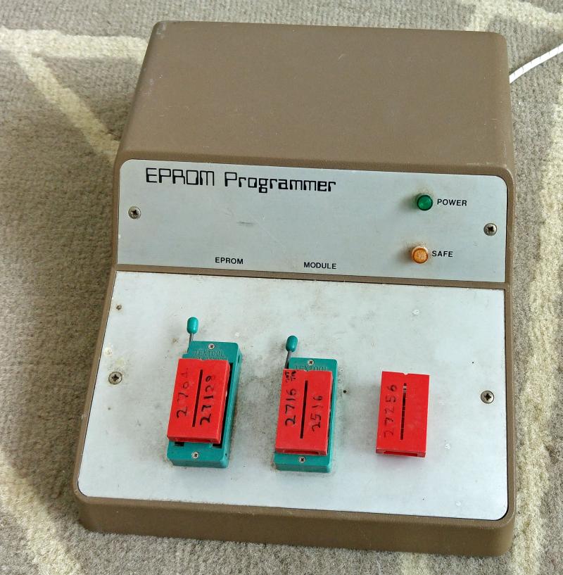
- Devices programmed : 2716, 2732, 2764, 27128, 27256, 27512
Programming voltages : 0, 5, 12.5, 21, 25 /30mA
Power supply voltages : 0, 5, 6 /200mA
Voltage selection : Automatic, by software.
Device selection : Plug-in modules to define device pinning.
Software:
- Written for : Expanded 1MHz Junior with 80 column terminal and DOS65
Written on : DOS65 using AS65.
Memory : Code and workspace $2000 – $2C00. Remaining ram is a buffer area for copying eproms to and from.
Functions : Device select, Program, Read, Buffer, Change memory
Hex/Ascii memory dump, Verify, Set buffer address,
Check device empty. Address parameters allowed.
Program speed: Up to 1K per 10 seconds.
Brief description
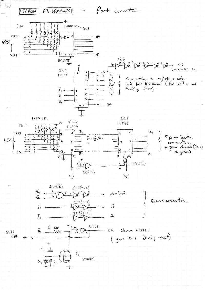
 Data is transferred to the eprom and the `registers’ of the programmer through port A of the VIA while port B controls the mode of port A and the PGM, OE and CS connections to the eprom. There are registers for setting the volts, and the upper and lower bytes of the eprom address. Each of these is formed from a pair of 74HC173 latches. The remaining digital circuit consists of a decoder (74HC138) some buffers and gates. Particular care has been taken to ensure that the latches are not triggered by noise. The eprom voltages are generated with 723 regulators with VFETs to change the voltage by switching in different resistors. The voltages can be switched in 300 microseconds allowing interactive programming techniques.
INTRODUCTION
In this article I describe a simple Eprom programmer which can be used with any computer which has a spare 65(C)22. Originally I designed it to work with the Junior but with the intention of making it adaptable to future computers such as DOS65. If used with the Junior it connects to the 6522 as an alternative to a printer. To add a 6522 to a 6XXX computer with an expansion bus is not too difficult but use of only one 6522 adds complexity to the design. To simplify matters plug-in modules containing wire links appropriate to the pin-outs of different eproms are necessary. This limitation should not matter to the amateur since only a small number of eproms have to be programmed. Some commercial programmers have plug-in modules or switches too. The present software (v1.0) runs on an expanded Junior with a 64K memory card. Adaptation to suit other computers is not difficult.
SPECIFICATION
Electrical:
   Power source .................... 9 to 12V/ 300mA DC from computer.
   Device selection ................ By software and plug in module.
   Eprom voltage selection ......... Programmable.
     				     Vpp = 0, 5, 12.5, 21, 25 Volts/ 30mA
				     Vcc = 0, 5, 6 Volts/ 200mA
Functions:
  *Read ............................ Copies eprom to ram.
  *Program ......................... Copies ram to eprom.
  *Verify .......................... Compares ram and eprom.
  *Base . .......................... Allows entry of first ram address.
  *Check ........................... Checks eprom empty.
   Device .......................... Allows selection of device type.
   Modify .......................... Allows ram contents to be altered.
   Hexdump ......................... Binary and Ascii dump of ram.
*Eprom address parameters allowed.
Devices which can be programmed:
2716/2516, 2532, 2732(A), 2564, 2764(A), 27128(A), 27256, NEC 27256D (21V), 27512. (2532, 2564 and 27512 untested).
The 27513 which has four pages of 16K has not been included, but it seems very likely that it could be programmed too.
Programming speed: The simple fast programming algorithm operates at a maximum rate of one kilobyte per 10 seconds (this is dependent on the type and condition of the device).
Indicators on programmer:
   Green LED ....................... Power on.
   Orange LED ...................... Safe. Do not remove eprom unless lit!
HARDWARE
The hardware falls into two sections. These are the programmable power supplies which generate programming and power supply voltages for the eprom and the digital logic.
In this PDF the circuit diagrams are shown.
 Functions of the 6522.
The 6522 has two ports, A and B, each having 8 input/output lines and two control lines which are normally used for handshaking. Control line CB1 enables the computer to sense that the programmer is connected and switched on. Data is written to the `registers’ of the programmer and read from and written to the eprom through port A. PB0, PB1 and PB2 select the mode of port
A. PB3 is an active high reset output. It floats high and resets all the programmer registers whenever the 6522 is reset. PB4 and PB5 are eprom control (EC) outputs which connect through inverters to OE, CS, A14, or A15 of the eprom. PB7 is the VIA monostable output which is used to provide programming pulses. Since VIA monostable pulses are always negative they do not suit all types of eprom. So PB6 is used to control their polarity with external logic.Before data can be written into a register the eprom programmer is `primed’ by selecting a dummy register in advance. The purpose of this is to improve noise immunity. The functions of the ports and registers are summarised below.
 *************************************************************
 *  PORT A BITS    .| 7 | 6 | 5 | 4 | 3 | 2 | 1 | 0 |        *
 *                 .                                         *
 *  REGISTERS      .                                         *
 *...........................................................*
 *                 .                                         *
 *  ADDRESS LOW    .  A7  A6  A5  A4  A3  A2  A1  A0         *
 *                 .                                         *
 *                 .     EPROM ADDRESS LINES                 *
 *...........................................................*
 *                 .                                         *
 *  ADDRESS HIGH   .  NC  NC  A13 A12 A11 A10 A9  A8         *
 *                 .                                         *
 *                 .     EPROM ADDRESS LINES                 *
 *...........................................................*
 *  EPROM DATA     .  D7  D6  D5  D4  D3  D2  D1  D0         *
 *  (READ)         .                                         *
 *                 .    EPROM DATA LINES                     *
 *...........................................................*
 *  EPROM DATA     .  D7  D6  D5  D4  D3  D2  D1  D0         *
 *  (WRITE)        .                                         *
 *                 .    EPROM DATA LINES                     *
 *...........................................................*
 *  VOLTS          .  V7  V6  V5  V4  V3  V2  V1  V0         *
 *    VPP=         .                                         *
 *       OFF       .  0   0   0   0   0                      *
 *        0        .  0   0   0   0   1                      *
 *        5        .  0   0   0   1   1                      *
 *       12.5      .  0   0   1   1   1                      *
 *       21        .  0   1   0   1   1                      *
 *       25        .  1   0   0   1   1                      *
 *                 .                                         *
 *    VCC=         .                                         *
 *       OFF       .                      0   0              *
 *        5        .                      0   1              *
 *        6        .                      1   1              *
 *                 .                                         *
 *    SAFE LAMP    .                                         *
 *       OFF       .                              0          *
 *       ON        .                              1          *
 *************************************************************
Table 1 – Port A functions.
 ************************************************************
 *  PORT B BITS      | 7 | 6 | 5 | 4 | 3 | 2 | 1 | 0 !      *
 *                                                          *
 *  PGM pulse        | X |                                  *
 *   active 0              0                                *
 *   active 1              1                                *
 *                                                          *
 *  Eprom control                                           *
 *     EC1=1                  0                             *
 *     EC1=0                  1                             *
 *     EC2=1                      0                         *
 *     EC2=0                      1                         *
 *                                                          *
 *  Reset (all registers cleared)     1                     *
 *  Operational                       0                     *
 *                                                          *
 *  Register select                                         *
 *    Prime                               0   0   0         *
 *    Write eprom                         0   0   1         *
 *    Read eprom                          0   1   0         *
 *   #Write Addr low                      0   1   1         *
 *   #Write Addr high                     1   0   0         *
 *   #Write volts                         1   0   1         *
 *    Unused                              1   1   0         *
 *    No selection                        1   1   1         *
 *                                                          *
 *   #must be primed with data ready on Port A              *
 *                                                          *
 ************************************************************
Table 2 – Port B functions.
The programmable power supplies.
Both programmable power supplies use 723 regulators with VFETS to switch different resistors into the dividers. Close tolerance resistors avoid the requirement for trimmers for each voltage. The VFETs can be driven directly from HCMOS outputs. There is current limiting at 30mA for Vpp and 200mA for Vcc. The vpp 0 volt setting is obtained by shorting the output to ground with
a T10. If the 6522 is reset this will rapidly occur. This is important because eproms are damaged if Vpp is present in the absence of Vcc. The high voltage (~30V) at the input of the programming voltage regulator is generated by a 78S40 inverter. Vcc is switched on by applying logic 1 to the base of T4, which turns on T3. Vpp works in a similar way. A time delay of about 20 milliseconds following switch on is required. Vcc may be switched between 5 and 6 volts, and Vpp between 0 (using T10 as a short), 5, 12.5, 21 and 25 volts in 300 micro-seconds, perhaps less. Note that T5 requires a heatsink.
Digital circuit.
The digital circuit is quite straight forward. The port lines from the 6522 are fully buffered. The pull-up resistors on port B cause these lines to float high whenever the 6522 is disconnected or reset, ensuring that the programmer is reset and preventing voltages appearing across the eprom socket. The 8 bit latches are made from pairs of 4 bit latches of type 74HC173. The register select lines of port B are decoded by IC2 (74HC138). The select line of the non-existent `prime’ register is connected to a sequence of gates (IC3) which
provides a delayed trigger edge when this register is deselected, by which time the appropriate latch will have been enabled. This time delay gives the latching circuit its noise immunity. On switch-on the circuit surrounding T1 causes the output of IC6(d) to go high and clears all the latches. This takes all the connections to the eprom to 0 volts. If PB3 is high the same happens. CB1 senses edges on the output of IC6(d) to allow the software to ascertain whether or not the programmer is connected and switched on. You must connect CB1 otherwise the software will
not work. However it is not always effective as the HCMOS output seems to become high impedance when the power is switched off and CB1 is triggered by noise. I think the addition of an emitter follower will cure this problem. But this is a minor point. Each of the signal connections to the eprom is made through a 470 ohm resistor to limit the current in the event of a wrong connection. If desired the digital IC’s can be protected from accidental connection to Vpp by the addition of 6V2 400mW zener diodes from their outputs to ground.
CONSTRUCTIONAL HINTS.
In this section I describe the constructional techniques which I employed, and in particular, a way of solving the awkward problem of mounting ZIF sockets on front panels. Also I have included details of socket and module wiring. The constructor can ignore this section entirely, if he wishes.
The case
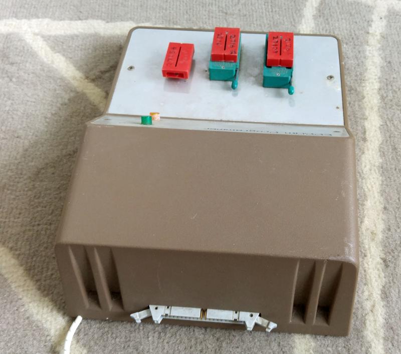
One of the first things to do is to choose a case to put it in. (If any). In my version this was Vero model 75-1715G, a plastic case with a sloping aluminium front panel. The case accommodates a large PCB (PCB 1) on which all the components are mounted and a small PCB (PCB 2) to which the eprom and module are attached.
The eprom and module sockets.
The modules are 24 pin DIL plugs with wire links to suit different devices. Eproms and modules are held in 28 pin and 24 pin zero insertion force (ZIF) sockets mounted on PCB 2. I used `ZETRONIX’ ZIF sockets because they can be dismantled and with suitable holes (3mm countersunk in base, 5mm in slider) bolted onto the aluminium panel leaving the pins protruding through slots. The PCB which has corresponding slots is bolted underneath the panel making the ends of the pins about level with its’ copper side. Reliable connections to tracks at the edges of the slots can be made with wire links. A 50 way transition connector is soldered to the copper side (by bending the pins over) and a 50 way ribbon cable is attached. The wires of the ribbon cable are used in pairs so there are only 25 connections, the Vcc, Vpp and ground connections are made separately. The ribbon cable attaches to PCB 1 with IDC connectors.
The main board (PCB 1).
All remaining components are soldered to PCB 1, which for ease of construction is single sided with a great many wire links. When designing the circuit layout possible decoupling problems must be borne in mind. It is advisable to distinguish between digital and analogue ground, preferably with these and the 0V connection to the eprom meeting at one point. Plenty of decoupling capacitors should be included.
Wiring of the 40 way connector.
Digital connections to the 6522 are made with 40 way ribbon cable attached by 40 way IDC connectors at each end. The wiring corresponds to the pin layout of a 6522, only CA1 and CA2 are out of sequence. Alternate wires of the cable are grounded to improve noise immunity.
Top view of right angle plug:


             ****************
             *               ****************
             * pin 1          ***********  *
             *             ***           **
             * CB2.   .0   *
             * CB1.   .0   *
             * PB7.   .0   *
             * PB6.   .0   *
             * PB5.   .0   *
             * PB4.   .0   *
             * PB3.   .0   *
             * PB2.   .0   *
             * PB1.   .0   *
             * PB0.   .0   *
             * CA2.   .0   *
             * CA1.   .0   *
             * PA7.   .0   *
             * PA6.   .0   *
             * PA5.   .0   *
             * PA4.   .0   *
             * PA3.   .0   *
             * PA2.   .0   *
             * PA1.   .0   *
             * PA0.   .0   *
             *             ***         **
             *      pin 40  ***********  *
             *              ***************
             **************
Table 3 – Eprom connections and voltages.
*******************************************************************************
        |                                   |                       |
Device  |     Eprom connections             |            Vpp        |Vcc prog
        | __________________________________________________________|
        | pulse  |   EC1  |   EC2  |  Vpp   | read  | prog  | before|
        |        |        |        |        |       |       | prog  |
________|________|________|________|________|_______|_______|_______|_________
        |        |        |        |        |       |       |       |
2716    | PGM/CS |  NC    |  OE    |  Vpp   |  5    |  25   |  5    |   5
        |        |        |        |        |       |       |       |
2732    | PGM/CS |  NC    |  NC    | OE/Vpp |  0    |  25   |  5    |   5
        |        |        |        |        |       |       |       |
2732A   | PGM/CS |  NC    |  NC    | OE/Vpp |  0    |  21   |  5    |   5
        |        |        |        |        |       |       |       |
2532    | CS     |  NC    |  NC    |  Vpp   |  5    |  25   |  5    |   5
        |        |        |        |        |       |       |       |
2764    | PGM    |  CS    |  OE    |  Vpp   |  5    |  21   |  5    |   6
        |        |        |        |        |       |       |       |
2764A   | PGM    |  CS    |  OE    |  Vpp   |  5    |  12.5 |  5    |   6
        |        |        |        |        |       |       |       |
2564    | PD/PGM |  CS1   |  CS2   |  Vpp   |  5    |  25   |  5    |   5
        |        |        |        |        |       |       |       |
27128   | PGM    |  CS    |  OE    |  Vpp   |  5    |  21   |  5    |   6
        |        |        |        |        |       |       |       |
27256   | PGM/CS |  A14   |  OE    |  Vpp   |  5    |  12.5 |  5    |   6
        |        |        |        |        |       |       |       |
27256D  | PGM/CS |  A14   |  OE    |  Vpp   |  5    |  21   |  5    |   6
        |        |        |        |        |       |       |       |
27512   | PGM/CS |  A14   |  A15   | OE/Vpp |  0    |  12.5 |  5    |   6
        |        |        |        |        |       |       |       |
*******************************************************************************
NC = No connection.
Vcc (Read) = 5 volts.
CS (Chip select) = CE (Chip enable).
To Eprom: To programmer electronics:
    To Eprom:                         To programmer electronics:

   Module pin  |  Eprom pin          Module pin  |  Connection
  _____________|____________         ____________|____________
               |                                 |
     1         |   1                   24        |   Vpp
     2         |   28                  23        |   Vcc
     3         |   2                   22        |   A12
     4         |   27                  21        |   Pulse
     5         |   26                  20        |   A13
     6         |   25                  19        |   A8
     7         |   24                  18        |   A9
     8         |   23                  17        |   A11
     9         |   22                  16        |   EC2
     10        |   21                  15        |   A10
     11        |   20                  14        |   EC1
     12        |   NC                  13        |   NC
  _____________|_____________       _____________|____________
Table – 4. Table – 5.
Module wiring.
The remaining pins (D0 – D7, A0 – A7 and ground) of the eprom socket are common to all the eproms. They are not, therefore, connected to the module, but directly to the eprom socket. Note that there is no connection to pin 13 of the module so that in the event of its accidental reversal Vpp is unconnected. Comparison with the pin layout of a 2764 or 27128 reveals that the links on the module for these devices go straight across (pin 1 to pin 24 etc) except that there is no link from pin 12 to pin 13.
The module wirings for different devices are as follows:
******************************************************************************
           PIN   | 1  | 2  | 3  | 4  | 5  | 6  | 7  | 8  | 9  | 10 | 11 | 12 |
_________________|____|____|____|____|____|____|____|____|____|____|____|____|
                 |    |    |    |    |    |    |    |    |    |    |    |    |
 2516/ 2716      | NC | NC | NC | NC | 23 | 19 | 18 | 24 | 16 | 15 | 21 | NC |
                 |    |    |    |    |    |    |    |    |    |    |    |    |
 2732/ 2732A     | NC | NC | NC | NC | 23 | 19 | 18 | 17 | 24 | 15 | 21 | NC |
                 |    |    |    |    |    |    |    |    |    |    |    |    |
#2532            | NC | NC | NC | NC | 23 | 19 | 18 | 24 | 14 | 15 | 17 | NC |
                 |    |    |    |    |    |    |    |    |    |    |    |    |
 2764/ 2764A     | 24 | 23 | 22 | 21 | 20 | 19 | 18 | 17 | 16 | 15 | 14 | NC |
 27128           |    |    |    |    |    |    |    |    |    |    |    |    |
                 |    |    |    |    |    |    |    |    |    |    |    |    |
#2564            | 24 | 23 | 14 | 16 | 23 | 19 | 18 | 22 | 21 | 15 | 17 | NC |
                 |    |    |    |    |    |    |    |    |    |    |    |    |
 27256/ 27256D   | 24 | 23 | 22 | 14 | 20 | 19 | 18 | 17 | 16 | 15 | 21 | NC |
                 |    |    |    |    |    |    |    |    |    |    |    |    |
#27512           | 16 | 23 | 22 | 14 | 20 | 19 | 18 | 17 | 24 | 15 | 21 | NC |
                 |    |    |    |    |    |    |    |    |    |    |    |    |
#Untested        |    |    |    |    |    |    |    |    |    |    |    |    |
******************************************************************************
Table – 6 Module wiring.
So for example on a 27512 module pin 1 connects with pin 16.
SOFTWARE
Two versions of the software are available: a ROMmable version for the Junior and as a DOS65 command.
Download here the sources of the Junior version , and here the DOS65 version.
I wrote the software for the Junior on DOS65 with its excellent 6502 assembler AS. The code can be stored in rom, provided the workspace is in ram. The usual load and execute address is $2000 and the code is just under 3K in length. Note that the timings are for a 1 MHz 6502. On running the program a list of commands is displayed. They work as follows:
(i) Base: This is the base address of the Juniors’ ram from which all read, program and verify commands start.
Syntax: B <xxxx>
where <xxxx> is the desired address. If the address is not supplied a
prompt is given.
(ii) Check: A routine to check that the eprom is empty is called.
Syntax: C <a1>,<a2>
where <a1> is the start address and <a2> the end address of the eprom.
The comma is optional unless <a1> is not supplied and <a2> is. In the
absence of parameters the start and end addresses of the eprom are
assumed.
(iii) Device: This allows selection of eprom type.
Syntax: D <l>
where <l> is a letter of the alphabet corresponding to the choice. If
<l> is not entered a menu of available types is printed.
(iv) Program: The ram area starting from base is copied to the eprom.
Syntax P <a1>,<a2>
(v) Read: The contents of the eprom are copied into ram starting at base.
Note that certain areas of ram cannot be overwritten (Normally $0000 to
$2FFF and $D000 to $FFFF) and an attempt to do so will produce an error
message. The 27512 has to be read with address parameters since its
length exceeds the length of the buffer.
Syntax: P <a1>,<a2>
(vi) Verify: The eprom contents between the parameters are compared to the
ram starting at base and differences are printed in blocks of 16.
Syntax: V <a1>,<a2>
(vii) Modify: The ram can be changed with this instruction.
Syntax: @ <xxxx>
where <xxxx> is an address. To escape from modify type <CR> on a blank line. <+> and <-> may be used to go forwards and backwards and new bytes can be typed in. Ascii characters can be entered if they are preceded by a quote. A number of bytes can be typed on one line. e.g.
Junior |Keyboard
|
3000 39 |23 45 76 ‘A ++++ <CR>
3008 20 |
(viii) Memory dump: The ram is listed in hexadecimal and ascii between the
addresses given.
Syntax: M <a1>,<a2>
(ix) Quit: Go to Junior monitor.
Syntax: Q
Examples:
B 3000 Base address = $3000
D A Device = 2716. (If the ‘A’ is omitted a list is printed).
P 0,7FF )
or P ) Copy ram $3000 to $37FF to entire eprom.
or P ,7FF )
or P 0 )
P 10F,10F Copy ram $3000 to eprom $10F, one address only
P 300,800 Error message, end of eprom exceeded.
R 100,1FF Copy eprom $100 to $1FF to ram $3000 to $30FF
NMI and keyboard breaks cause the programmer to be reset and an abort message produced. The vectors are restored to their original values on quitting. The requirements of the terminal are the same as those for Micro-Ade, i.e. it has to keep a local copy on the screen of characters typed from the keyboard and accept LF, CR and DEL control codes.
A 2MHz DOS65 version of the software has an additional `!’ command to call other programs in a similar way to EDITOR. So for example to save a block of memory you would type: !save filename 3000,37FF. However this awaits the construction of a 6522 card with a 40 way IDC plug, and perhaps with 64K of ram (2×62656).
A FINAL NOTE.
The eprom programmer which I have described has worked reliably for some months and the hardware worked first time, apart from a minor decoupling problem. A careful constructor ought to be confident that he can make it work, perhaps with one or two changes and improvements. Furthermore he can make use of existing software. If anyone finds any bugs in the software, errors in this
article or makes improvements I would like to hear about them.