
Publications Number 6500-15B
KIM-1
MICROCOMPUTER MODULE
USER MANUAL
AUGUST 1976
The information in this manual has been reviewed and is believed to be entirely reliable. However,
no responsibility is assumed for inaccuracies. The material in this manual is for informational
purposes only and is subject to change without notice.
Second Edition
© MOS TECHNOLOGY, INC. 1976
"All Rights Reserved"
MOS TECHNOLOGY, INC.
950 Rittenhouse Road
Norristown, PA 19401
TABLE OF CONTENTS CHAPTER I YOUR KIM-1 MICROCOMPUTER MODULE 1 CHAPTER 2 GETTING STARTED 5 www.kim-1.com/usrman.htm 2.1 Parts Complement 5 2.2 A Few Words of Caution! 6 2.3 First Steps 6 2.4 Let's Try a Simple Problem 9 2.5 Adding an Audio Tape Unit 12 2.6 Adding a Teleprinter 17 CHAPTER 3 THE KIM-1 SYSTEM 21 3.1 KIM-1 System Description 21 3.2 KIM-1 Memory Allocation 34 3.3 KIM-1 Operating Programs 40 CHAPTER 4 OPERATING THE KIM-1 SYSTEM 43 4.1 Using the Keyboard and Display 43 4.2 Using the Audio Tape Unit 47 4.3 Using the Teleprinter 50 CHAPTER 5 LET'S TRY A REAL APPLICATION 55 5.1 Defining the Interface 55 5.2 Writing the Program 58 5.3 Entering the Program 65 5.4 Executing the Program 66 5.5 Program Debugging and Modification 67
ii
CHAPTER 6 EXPANDING YOUR SYSTEM 71 6.1 Memory and I/O Expansion 71 6.2 Interrupt Vector Management 75 CHAPTER 7 WARRANTY AND SERVICE 79 7.1 In-Warranty Service 79 7.2 Out-of-Warranty Service 80 7.3 Policy on Changes 80 7.4 Shipping Instructions 80
iii
LIST OF FIGURES CHAPTER 2 2-1 KIM MODULE 7 2-2 Power Supply Connections 8 2-3 Audio Tape Unit Connections 13 2-4 TTY Connections 18 CHAPTER 3 3-1 KIM-1 Block Diagram 24 3-2 Detailed Block Diagram 25 3-3 Control and Timing 26 3-4 1K x 8 RAM Memory 27 3-5 Keyboard and Display 28 3-6 Keyboard Detail 29 3-7 TTY Interface 30 3-8 Audio Tape Interface 31 3-9 Application Connector 32 3-10 Expansion Connector 33 3-11 Memory Block Diagram 37 3-12 Memory Map 38 3-13 Special Memory Addresses 39 3-14 Flow Chart 41 CHAPTER 5 5-1 Speaker Application 57 5-2 Assembly Language Listing 60 5-3 Square Wave Output 62 5-4 Machine Language Code Table 63 5-5 Key Sequence: Enter Program 65 CHAPTER6 6-1 4K Expansion 73 6-2 65K Expansion 74 6-3 Vector Selection 78
iv
LIST OF APPENDiCES APPENDIX A KIM-1 Parts List A-1 APPENDIX B KIM-1 Parts Location B-1 APPENDIX C In Case of Trouble C-1 APPENDIX D Suggested Power Supply D-1 APPENDIX E Audio Tape Format E-1 APPENDIX F Paper Tape Format F-1 APPENDIX G 6502 Characteristics G-1 APPENDIX H 6530 Characteristics H-1 APPENDIX I KIM-1 Program Listings I-1 Congratulations and welcome to the exciting new world of micro- computers! As the owner of a KIM-1 Microcomputer Module, you now have at your disposal a completely operational, fully tested, and very capable digital computer which incorporates the latest in microprocessor tech- nology offered by MOS Technology, Inc. By selecting the KIM-1 module, you have eliminated all of the problems of constructing and debugging a microcomputer system. Your time is now available for learning the opera- tion of the system and beginning immediately to apply it to your specific areas of interest. In fact, if you will follow a few simple procedures outlined in this manual, you should be able to achieve initial operation of your KIM-1 module within a few minutes after unpacking the shipping container. Your KIM-1 module has been designed to provide you with a choice of operating features. You may choose to operate the system using only the keyboard and display included as part of the module. Next, you may add a low cost audio cassette tape recorder to allow storage and retrieval of your programs. Also, you may add a serial interfaced teleprinter to the system to provide keyboard commands, hard-copy printing, and paper tape read or punch capability.
1
At the heart of your KIM-1 system is an MCS 6502 Microprocessor Array operating in conjunction with two MCS 6530 arrays. Each MCS 6530 provides a total of 1024 bytes of Read-only Memory (ROM) , 64 bytes of Random Access Memory (RAM), 15 Input/Output pins, and an Interval Timer. Stored permanently in the ROM's of the MCS 6530 arrays are the monitor and executive programs devised by NOS Technology, Inc. to control the various operating modes of the KIM-1 system. The KIM-1 system is intended to provide you with a capable micro- computer for use in your real-world" application. Accordingly, the system includes a full 1024 bytes of RAM to provide data and program storage for your application program. In addition, you are provided with 15 bidirectional input/output pins to allow interface control of your specific application. Finally, one of the interval timers included in the system is available for generation of time base signals required by your application. Your KIM-1 system comes to you complete with all components mounted and tested as a system. You need not worry about timing signals (we've included a 1MHz crystal oscillator on the module), interface logic or levels between system components, or interface circuitry to peripheral devices. In fact, you need only apply the indicated power supply voltages to the designated pins to achieve full operation of your KIM-1 system. We recommend that you read all of this manual before applying power to or attempting to operate your KIM-1 module. In the order presented, you will find: Chapter 2 - "hints and kinks" to help you achieve initial system operation Chapter 3 - a more detailed description of the KIM-1 system hardware and software Chapter 4 - operating procedures for all system modes Chapter 5 - an example of a typical application program using all of the features of the KIM-1 system.
2
At some future time, you may find it desirable to expand the KIM-1 system to incorporate more memory, different types of memory, or addi- tional input/output capability. Again, we have tried to make system expansion as simple as possible with all required interface signals brought out to a special connector on the module. Watch for: Chapter 6 - a guide to system expansion for increasing both memory and input/output capability Despite our best efforts to provide you with a fully operable and reliable system, you might encounter some difficulties with your KIM-1 module. If so, refer to: Chapter 7 - some guidance on warranty and service procedures for your KIM-1 module Following the basic text of this manual, you will find a series of Appendices intended to provide you with detailed information on certain specialized subjects of interest to you in understanding the operation of the KIM-1 system. Lastly, since this manual cannot presume to provide all of the technical information on the hardware or programming aspects of the MCS 6502 microprocessor array, we are including with your KIM-1 system two additional manuals for your reference. The Hardware Manual defines the various elements of the system, their electrical and interface characteristics, and the basic system architecture and timing. The Programming Manual provides the detailed information required to write effective programs using the MCS 6502 instruction program set. So much for introductory comments! Now lets get started and see if we can get your KIM-1 Microcomputer Module doing some real work for you. This chapter is intended to guide you through the first important steps in achieving initial operation of your KIM-1 Microcomputer Module. We will ask you to perform certain operations without explanation at this time as to why they are being done. In later sections of this manual, full explanations will be offered for every operating procedure. 2.1 PARTS COMPLEMENT After unpacking the shipping container for your KIM-1, you should have located the following items: 3 Books - KIM-1 Users Manual Hardware Manual Programming Manual 1 Programming Card 1 System Schematic 1 KIM-1 Module 1 Connector (Already mounted on the Module) 1 Hardware Packet 1 Warranty Card You may wish to save the shipping container and packing material should you need to return your KIM-1 module to us at some future date.
5
2.2 A FEW WORDS OF CAUTION
WARNING
Your KIM-1 module includes a number of MOS integrated circuits. All such
circuits include protective devices to prevent damage resulting from
inadvertant application of high voltage potentials to the pins of the
device. However, normal precautions should be taken to prevent the appli-
cation of high voltage static discharges to the pins of an MOS device.
Immediately before removal of the packing material from your KIM-1 module,
you should develop the following precautionary habits:
1. Discharge any static charge build up on your body by touching a
ground connection before touching any part of your KIM-1 module.
(This precaution is especially important if you are working in a
carpeted area)
2. Be certain that soldering irons or test equipment used on the
KIM-1 module are properly grounded and not the source of
dangerously high voltage levels.
On a different subject, after unpacking your KIM-1 module, you will
note the presence of a potentiometer. This adjustment has been set at
the factory to insure correct operation of the audio cassette interface
circuits. It should never be necessary for you to change the position of
this potentiometer. ------
2.3 FIRST STEPS
After unpacking the KIM-1 module, locate the small hardware packet
and install the rubber pads provided. The rubber pads are located at the
bottom of the module (see attached sketch) and act both to lift the card
off your work surface and to provide mechanical support for the module
while you depress keys.
6
Place the module such that the keyboard is to your lower right and observe that two connector locations extend from the module to your left. The connector area on the lower left is referred to as the Application connector (A). You will note that a 44 pin board edge connector is already installed at this location. The connector area to the upper left is for use by you for future system expansion and is referred to as the Expansion connector (E).
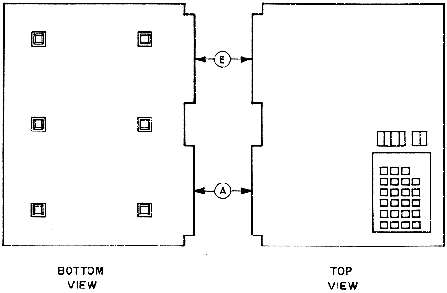 KIM-1 Module
FIGURE 2.1
7
KIM-1 Module
FIGURE 2.1
7Remove the (A) connector from the module and connect the pins as shown in the sketch.
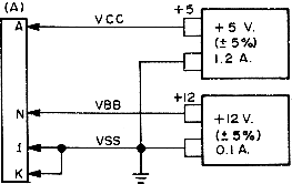 Power Supply Connections
FIGURE 2.2
Power Supply Connections
FIGURE 2.28
Now, recheck your connections, turn on your power supplies, and depress [RS] (reset). You should see the LED display digits light as your first check that the system is operational. If not, recheck your hookup or refer to Appendix C (In Case of Trouble). 2.4 LETS TRY A SIMPLE PROGRAM Assuming that you have completed successfully all of the steps thus far, a simple program now can be tried to demonstrate the operation of the system and increase your confidence that everything works properly. We'll be using only the keyboard and display on the module for this example. (In the next two sections we'll worry about the teleprinter and the audio cassette). For our first example, we will add two 8 bit binary numbers together and display the result. We presume that you are familiar with the hex- adecimal representation of numbers and the general rules for binary arith- metic. First check and be sure that the slide switch in the upper right corner of the keyboard is pushed to the left (SST Mode is OFF). Now proceed with the following key sequence: Press Keys See On Display Step # [AD] xxxx xx 1 [0] [0] [0] [2] 0002 xx 2 [DA] 0002 xx 3 [1] [8] 0002 18 4 [+] [A] [5] 0003 A5 5 [+] [0] [0] 0004 00 6 [+] [6] [5] 0005 65 7 [+] [0] [1] 0006 01 8 [+] [8] [5] 0007 85 9 [+] [F] [A] 0008 FA 10 [+] [A] [9] 0009 A9 11 [+] [0] [0] 000A 00 12 [+] [8] [5] 000B 85 13 [+] [F] [B] 000C FB 14 [+] [4] [C] 000D 4C 15 [+] [4] [F] 000E 4F 16 [+] [1] [C] 000F 1C 17
9
What you have just done is entered a program and stored it in the RAM at locations 0002 through QOOF. You should have noticed the purpose of several special keys on your keyboard: [AD] - selects the address entry mode [DA] - selects the data entry mode [+] - increments the address without changing the entry mode [0] to [F] - 16 entry keys defining the hex code for address or data entry You've noticed as well that your display contains 6 digits. The four on the left are used to display the hex code for an address. The two on the right show the hex code for the data stored at the address shown. Therefore, when you pressed [AD] (step 1) and [0] [0] [0] [2] (step 2), you defined the address entry mode, selected the address 0002, and displayed the address 0002 in the four left-most display digits. Incidentally, when we show an "x" in the display chart, we mean that we don't know what will be displayed and we "don't care." Next you pressed [DA] (step 3) followed by [1] [8] (step 4). Here, you have defined the data entry mode and entered the value 18 to be stored at your selected address 0002. Of course, the 18 then was dis- played in the two right-most digits of your display. You remained in the data entry mode but began to press [+] followed by a two digit number (steps 5 to 17). Note that each depression of the [+] key caused the address displayed to increase by one. The hex keys following the [+] key continued to enter the data field of the display. This procedure is merely a convenience when a number of successive address locations are to be filled. If you made any mistakes in pressing the keys, you should have noticed that correcting an error is simply a matter of reentering the data until the correct numbers show on the display.
10
The program you have entered is a simple loop to add two 8 bit binary numbers together and present the result on the display. For a programmer, the listing of the program entered might appear as follows: POINTL = $FA POINTH = $FB START = $1C4F 0000 VALl 0001 VAL2 0002 18 PROG CLC 0003 A5 00 LDA VALl 0005 65 01 ADC VAL2 0007 85 FA STA POINTL 0009 A9 00 LDA #00 000B 85 FB STA POINTH 000D 4C 4F 1C JMP START Stated in simple terms, the program will clear the carry flag (CLC) load VALl into the accumulator (LDA VALl), add with carry VAL2 to the accumulator (ADC VAL2), and store the result in a location POINTL (STA POINTL). A zero value is stored in a location POINTH (LDA #00 and STA POINTH) and the program jumps to a point labelled START (JMP START). This pre-stored program will cause the display to be activated and will cause the address field of your display to show the numbers stored in locations POINTH and POINTL. Note that the result of the addition has already been stored in location POINTL. The hex codes appearing next to the address field of the listing are exactly the numbers you entered to store the program. We refer to these as machine language codes. For example, 4C is the hex code for the JMP instruction of the microprocessor. The next two bytes of the program define 1C4F (START) as the jump address. As yet, you are not able to run the program because you have not yet entered the two variables (VALl and VAL2). Lets try an actual example: Press Keys See On Display Step # [AD] 000F 1C 17A [0] [0] [F] [1] 00F1 xx 17B [DA] [0] [0] 00F1 00 18 [AD] 00F1 00 19 [0] [0] [0] [0] 0000 xx 20 [DA] 0000 02 21 [+] [0] [3] 0001 03 22 [+] [GO] 0002 18 23
11
Steps 17A, 17B, and 18 insure that the binary arithmetic mode is selected. Steps 19 to 21 store the hex value 02 in location 0000 (VAL1). Step 22 stores the hex value 03 in location 0001 (VAL2). Now we are ready to run the program. In step 23, the [GO] key causes the program to execute and the result, 05, appears in the right two digits of the address display. Although the problem appears triviAL, it illustrates the basic principles of entering and executing any program as well as providing a fairly high assurance level that your KIM-1 module is operating properly. You should try one more example using your stored program. Repeat steps 17A to 23 but substitute the value FF for VALl and VAL2 at locations 0000 and 0001. Now when you press the GO key, your display should read: 00FE xx The answer is correct because: FF = 1111 1111 + FF = 1111 1111 FE 1111 1110 Try some more examples if you wish and then let's move on to the rest of the system. 2.5 ADDING A TAPERECORDER In the previous section, you entered and executed a program. If you turn off the power supplies to the system, your program is lost since the memory into which you stored your program is volatile. If you require the same program again, you would have to repower the system and reenter the program as in the previous example. The KIM-1 system is designed to work with an audio cassette tape recorder/player to provide you with a medium for permanent storage of your programs or data. The cassette with recorded data may be reread by the system as often as you wish. In this section, you will connect the audio cassette unit to the system and verify its operation.
12
The recording technique used by the KIM-1 system and the interface circuits provided have been selected to insure trouble-free operation with virtually any type and any quality level audio cassette unit. (We have demonstrated correct operation with a tape unit purchased for less than $20.00 from a local discount outlet). In addition, tapes recorded on one unit may be played back to the system on a different unit if desired. We recommend, of course, that you make use of the best equip- ment and best quality tapes you have available. In selecting a tape unit for use with your KIM-1 system, you should verify that it comes equipped with the following features: 1. An earphone jack to provide a source of recorded tape data to the KIM-1 system. 2. A microphone jack to allow recording of data from the KIM-1 system on the tape. 3. Standard controls for Play, Record, Rewind, and Stop. Note: You should avoid certain miniaturized tape equipment intended for dictating applications where the microphone and speaker are enclosed within the unit and no connections are provided to external jacks. If such equipment is used, you will have to make internal modifications to reach the desired connection points. To connect your tape unit to the KIM-1 module, turn off the power supplies and remove the connector (A) from the module. Add the wires shown in the sketch:
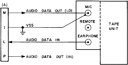 Audio Tape Unit Connections
FIGURE 2.3
13
Audio Tape Unit Connections
FIGURE 2.3
13Keep the leads as short as possible and avoid running the leads near sources of electrical interference. The connections shown are for typical, portable type units. The Audio Data Out (LO) signal has a level of approx- imately 15 mv. (peak) at pin M. Should you desire to use more expensive and elaborate audio tape equipment, you may prefer to connect the high level (1 volt peak) audio signal available at pin P to the "LINE" input of your equipment. Return the connector (A) to its correct position on the KIM-1 module and turn on the power supplies. To verify the operation of your audio cassette equipment, try the following procedures: 1. Reenter the sample program following the procedures outlined in the previous section (2.4). Try the sample problem again to be sure the system is working correctly. 2. Install a cassette in your tape equipment and REWIND to the limit position. 3. Define the starting and ending address of the program to be stored and assign an identification number (ID) to the program. Press Keys See On Display Step # [AD] xxxx xx 1 [0] [0] [F] [1] 00F1 xx 2 [DA] [0] [0] 00F1 00 3 [AD] 00F1 00 4 [1] [7] [F] [5] 17F5 xx 5 [DA] [0] [0] 17F5 00 6 [+] [0] [0] 17F6 00 7 [+] [1] [0] 17F7 10 8 [+] [0] [0] 17F8 00 9 [+] [0] [1] 17F9 01 10 [AD] 17F9 01 11 [1] [8] [0] [0] 1800 xx 12 You will recall that the program we wish to store on tape was loaded into locations 0000 to OOOF of the memory. Therefore, we define a start- ing address for recording as 0000 and store this in locations 17F5 and 17F6 (Steps 4 to 7). We define an ending address for recording as one more than the last step of our program and stored the value 0010 (= 000F + 1) in locations 17F7 and 17F8 (Steps 8,9). Finally we pick an arbitrary ID as 01 and store this value at location 17F9 (Step 10). Note that before we use the audio cassette unit for recording or playing back, we must put 00 in location 00F1 (Steps 1,2 and 3).
14
The starting address of the tape recording program is 1800. In Steps 11 and 12 we set this address value into the system. If we were to press [GO], the system would proceed to load data on to the magnetic tape. But first, we'd better start the tape! 4. Select the Record/Play mode of the tape recorder. Wait a few seconds for the tape to start moving and now: Press [GO] 5. The display will go dark for a short time and then will relight showing: 0000 xx 6. As soon as the display relights, the recording is finished and you should STOP the tape recorder. Now, you should verify that the recording has taken place correctly. This can be proven by reading the tape you have just recorded. Proceed as follows: 1. Rewind the tape cassette to its starting position. 2. Turn off the system power supplies and then later, turn them back on. This has the effect of destroying your previously stored program which you already have recorded on tape. 3. Prepare the system for reading the tape as follows: Press Keys See On Display Step # [RS] [AD] xxxx xx 1 [0] [0] [F] [1] 00F1 xx 2 [DA] [0] [0] 00F1 00 3 [AD] 00F1 00 4 [1] [7] [F] [9] 17F9 xx 5 [DA] 17F9 xx 6 [0] [1] 17F9 01 7 [AD] 17F9 01 8 [1] [8] [7] [3] 1873 xx 9 [GO] (Dark) 10
15
The KIM-1 system is now looking for tape input data with the ID label 01. Recall that this is the same ID label we assigned when we recorded the program. 4. If your tape unit has a volume control, set the control at approximately the half way point. 5. If your tape unit has a tone control, set the control for maximum treble. 6. Now, turn on the tape using the PLAY mode. The tape will move forward and the system will accept the recorded data. As soon as the data record (ID=01) has been read, the display should relight showing: 0000 xx You may now stop the tape unit. If the display relights and shows; FFFF xx this means that the selected record has been located and read but that an error has occurred during the reading of the data. In this case, press the [RS] key and repeat the read tape procedures from the beginning. If the FFFF still shows on the display, repeat the entire recording and play- back procedures checking each step carefully. If the problem persists, refer to Appendix C, (In Case of Trouble). If the tape continues to run and the display does not relight, this means that the system has been unsuccessful in reading any data back from the tape. In this case, repeat the entire recording and playback proce- dures checking each step carefully. If the problem persists, refer to Appendix C, (In Case of Trouble). 7. Assuming that you have read the tape successfully, you now may verify that the program has been restored to memory by trying a sample problem. (02 + 03 = 05) NOTE: The KIM-1 interface circuits for the audio tape system are designed so that you do not require special test equipment to set up correct operating levels. If you have followed the procedures indicated, the tape system should work without the need of any adjustments by you.
16
2.6 ADDING A TELEPRINTER If you have access to a serial teleprinter, you may add such a unit to the KIM-1 system with very little effort. One of the more commonly available units of this type is the Teletype Nodel 33ASR which we will use for the purposes of illustration in this section. However, if you have available different equipment, you may use the information presented here as a guide to connecting your specific unit. In any case, we recom- mend you follow the directions offered by the equipment manufacturer in his instruction manual to effect the desired wiring and connection options. The KIM-1 provides for a 4 wire interface to the TTY. Specifically, the "20 mA loop" configuration should be used and you should check that your TTY has been wired for this configuration. If not, you may easily change from "60 mA loop" to "20 mA loop" configurations following the manufacturers directions. The KIM-1 has been designed to work properly only with a teleprinter operating in full duplex mode. Check the literature supplied with your teleprinter if you are unsure if your unit is properly configured. You are not restricted to units with specific bit rates (10 CPS for TTY) since the KIM-1 system automatically adjusts for a wide variety of data rates (10CPS, 15CPS, 30CPS, etc.). To connect the TTY to the system, proceed as follows: 1. Turn off system power and remove connector (A) from the module. 2. Add the wires shown in the sketch to connector (A) and to the appropriate connector on the TTY unit. 3. The jumper wire from A-21 to A-V is used to define for the KIM-1 system that a teleprinter will be used as the only input/display device for the system. If you expect to use both TTY and the KIM-1 keyboard/display, you should install the switch shown instead of the jumper. Now, the switch, when open, will allow use of the keyboard and display on the KIM-1 module and, when closed, will select the tele- printer as the input/display device. (of course, you may use a clip-lead instead of the switch if you desire). 4. Be sure pins A-21 and A-V are connected. Reinstall con- nector (A) and return power to the system. Turn-on the TTY. 5. Press the [RS] key on the KIM-1 module then press the [RUB OUT] key on the TTY. This step is most important since the KIM-1 system adjusts automatically to the bit rate of the serial teleprinter and requires this first key depression to establish this rate.
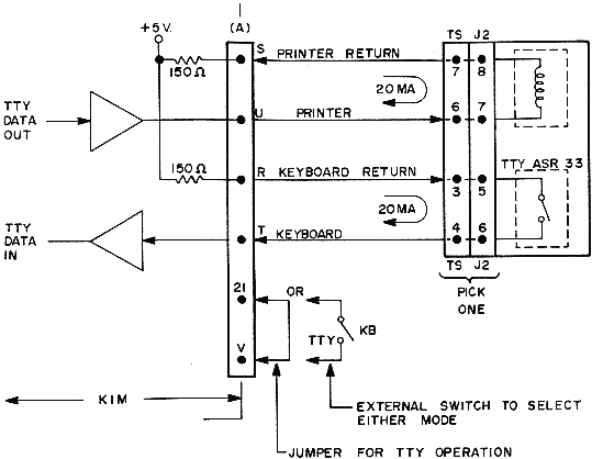 TTY Connections
FIGURE 2.4
TTY Connections
FIGURE 2.418
If everything is working properly you should immediately observe a message being typed as follows: KIM This is a prompting message telling you that the TTY is on-line and the KIM-1 system is ready to accept commands from the TTY keyboard. Should the prompting message not be typed press the [RS] key on the KIM-1 keyboard and then the [RUB OUT] key on the TTY. If the "KIM" message still is not typed, recheck all connections and the TTY itself and try again. If the problem persists, refer to Appendix C, (In Case of Trouble). 6. Assuming that the TTY is operable, you may now try a simple group of operations to verify correct system operation: Press Keys See On Display Step # KIM xxxx xx 1 0002 0002 2 [SPACE] 0002 xx 3 18. 18. 4 0003 xx 5 A5. A5. 6 0004 xx 7 [LF] 0003 A5 8 [RUB OUT] KIM xxxx xx 9 Step 1 shows the "KIM" prompting message. In Step 2, an address (0002) is selected followed by a space key in Step 3. The address cell 0002 together with the data stored at that location (xx) is printed. Step 4 shows the "modify cell" operation using the [.] key and the hex data keys preceding. Step 5 shows the incrementing to the next address cell (0003) after the [.] key. Note that the modification of cell 0002 also occurs. Steps 6 and 7 show the modification of data in cell 0003 and the incrementing to cell 0004. Step 8 shows the action of the [LF] key in backing up one cell to 0003 where we can see from the printout that the correct data (A5) has been stored at that location. Step 9 shows the reaction to the [RUB OUT] key in resetting the system and producing a new "KIM" prompting message. Note, by the way, that in this example you have repeated a portion of the program entry exactly as you did in Section 2.4 but this time using the TTY.
19
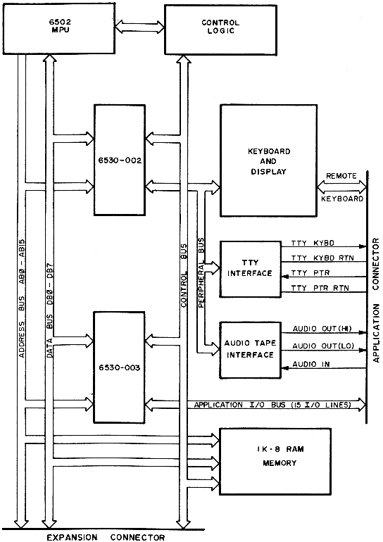
So much for now! If all of the operations have occurred properly, you may be certain that your TTY and KIM-1 module are working together correctly. We will describe in detail all of the other operations pos- sible with the TTY in a later section of the manual. If you have reached this point without problems, you now have completed all of the required system tests and may be confident that the KIM-1 module and your peripheral units are all working correctly. Our next task is to learn more about the KIM-1 system and its operating programs. Up to this point you have been engaged in bringing up your KIM-1 system and verifying its correct operation. Now it's time to learn more about the various parts of the KIM-1, how the parts work together as a system, and how the operating programs control the various activities of the system. The diagrams included in this section together with your full sized system schematic will be helpful in understanding the elements of your KIM-1 module. 3.1 KIM-1 SYSTEM DESCRIPTION Figure 3-1 shows a complete block diagram of the KIM-1 system. You should note first the presence of the MCS 6502 Microprocessor Array which acts as the central control element for the system. This unit is an 8 bit microprocessor which communicates with other system elements on three separate buses. First, a 16 bit address bus permits the 6502 to address directly up to 65,536 memory locations in the system. Next, an 8 bit, bidirectional data bus carries data from the 6502 array to any memory location or from any memory location back to the 6502 array. Lastly, a control bus carries various timing and control signals between the 6502 array and other system elements.
21
Associated with the 6502 array is a 1 MHz crystal which operates with an oscillator circuit contained on the 6502 array. This crystal control- led oscillator is the basic timing source from which all other system timing signals are derived. In particular, the þ2 signal generated by the 6502 array and used either alone, or gated with other control signals, is used as the system time base by all other system elements. The 6502 microprocessor is structured to work in conjunction with various types of memory. In the KIM-1 system, all memory may be consid- ered to be of the Read-only (ROM) or Read/Write (RAM) variety. The ROM portion of the memory provides permanent storage for the operating progams essential to the control of the KIM-1 system. You will note the inclusion of two devices, labelled 6530-002 and 6530-003. Each of these devices include a 1024 byte (8 bits per byte) ROM with different portions of the operating program stored permanently in each ROM. RAM type memory is available at three locations in the system. Again, each of the 6530 arrays include 64 bytes of RAM primarily used for temporary data storage in support of the operating program. In addition, a separate 1024 byte RAM is included in the KIM-1 system and provides memory storage for user defined application programs and data. Input/output controls for the system also are included within the 6530 arrays. Each 6530 array provides 15 I/O pins with the microprocessor and operating program defining whether each pin is an input pin or output pin, what data is to appear on the output pins, and reading the data appear ing on input pins. The I/O pins provided on the 6530-002 are dedicated to interfacing with specific elements of the KIM-1 system including the key- board, display, TTY interface circuit, and audio tape interface circuit. The 15 I/O pins on the 6530-003 are brought to a connector and are avail- able for the user to control a specific application.
22
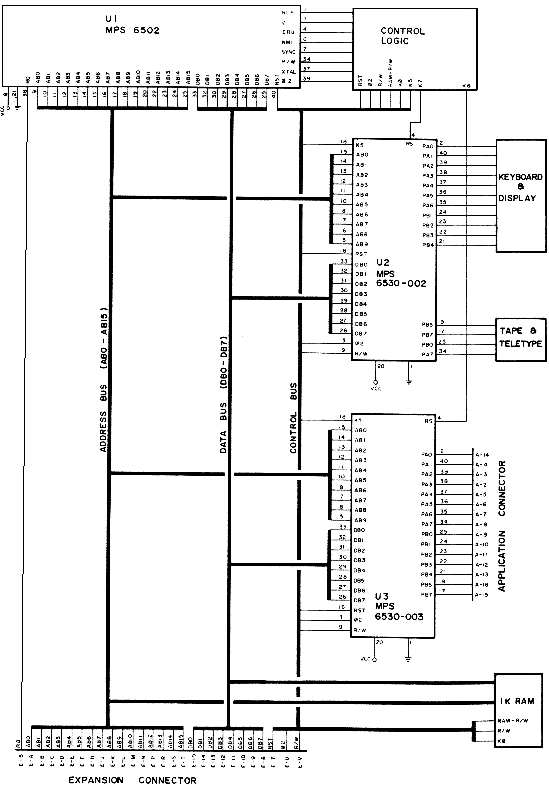
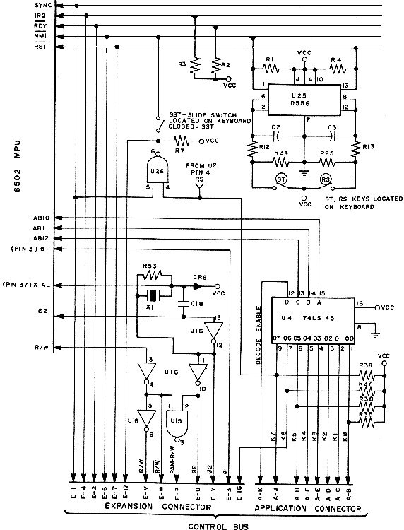
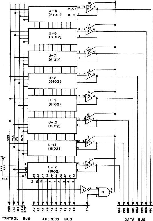
Finally, each 6530 array includes an interval timer capable of count- ing a specific number of system clocks to generate precise timing gates. The exact time interval is preset under program control. The interval timer on the 6530-003 array is available for a user defined application program and is not required by the operating programs. Figure 3-1 shows a major block labelled Control Logic. Included under this category are an address decoder used for generation of chip select signals for the 6530 arrays and the static RAM. Also included is the logic required to debounce the keys for system reset (RS key) and pro- gram stop (ST key). Lastly, special logic is included to allow operation of the system in a "single instruction" mode to facilitate program de- bugging. Figure 3-1 shows the keyboard/display logic interfacing with the I/O pins of the 6530-002. Also shown are the interface circuits for trans- mission of data to and reception of data from the TTY and audio tape units. Figure 3-2 shows the detailed interconnections between the MCS 6502 and the two NCS 6530 arrays. Figure 3-3 shows detailed logic and schematics for the control logic. Figure 3-4 shows a detailed schematic of the static RAM. Figure 3-5 and 3-6 show the detailed schematic of the keyboard and display logic and circuits. Figure 3-7 details the schematic of the TTY interface circuits. Figure 3-8 details the schematic of the audio tape cassette interface circuits. Figures 3-9 and 3-10 provide a summary of all signals available on either the Application connector or the Expansion Connector. The fold-out system schematic shows all of the elements of the system connected together and all signals appearing on the module connectors. You may refer to the Hardware Manual included with your KIM-1 module for additional details on the operating characteristics of the 6502 and 6530 arrays as well as detailed information on system timing.
23
 KIM-1 Block Diagram
FIGURE 3.1
24
KIM-1 Block Diagram
FIGURE 3.1
24
 Detailed Block Diagram
FIGURE 3.2
25
Detailed Block Diagram
FIGURE 3.2
25
 Control and Timing
FIGURE 3.3
26
Control and Timing
FIGURE 3.3
26
 1Kx8 RAM Memory
FIGURE 3.4
27
1Kx8 RAM Memory
FIGURE 3.4
27
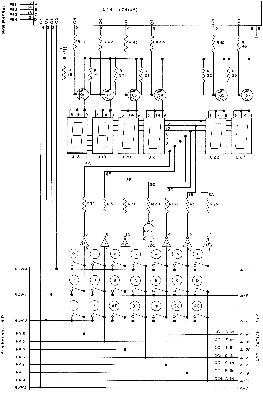 Keyboard and Display
FIGURE 3.5
28
Keyboard and Display
FIGURE 3.5
28
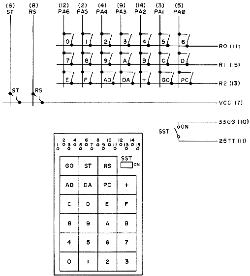 Keyboard Detail
FIGURE 3.6
29
Keyboard Detail
FIGURE 3.6
29
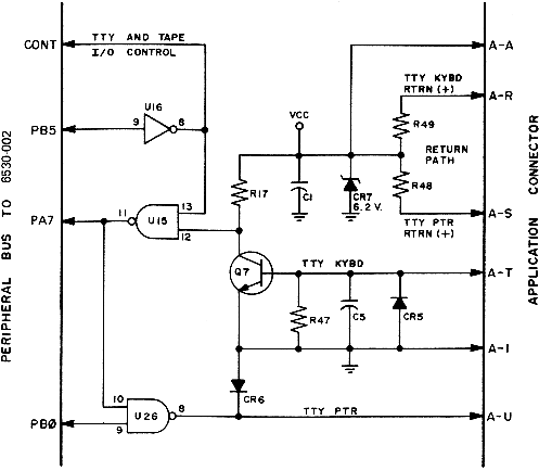 TTY Interface
FIGURE 3.7
30
TTY Interface
FIGURE 3.7
30
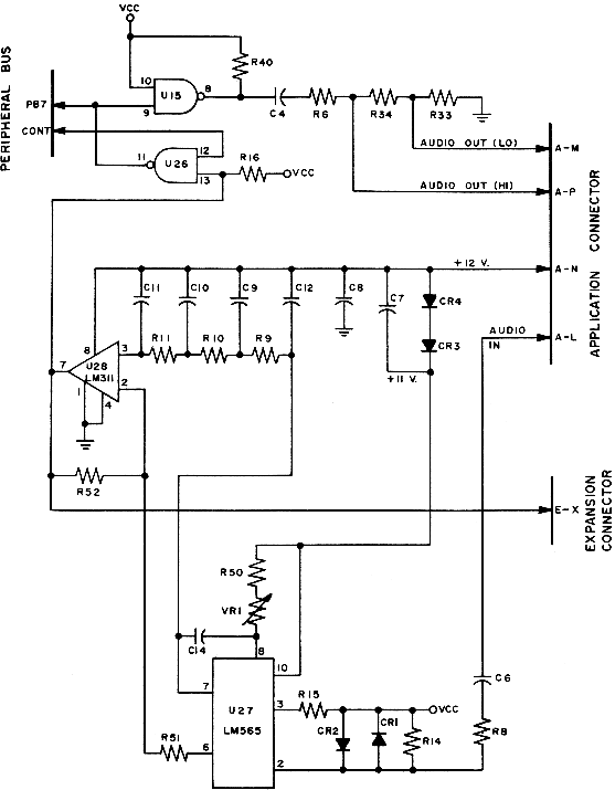 Audio Tape Interface
FIGURE 3.8
31
Audio Tape Interface
FIGURE 3.8
31
| 22 | KB Col D | | 0 | KB Row 1 | | 21 | KB Col A | | Y | KB Col C | | 20 | KB Col E | | X | KB Row 2 | | 19 | KB Col B | | W | KB Col G | | 18 | KB Col F | | V | KB Row 3 | | 17 | KB Row 0 | | U | TTY PTR | | 16 | PB5 | | T | TTY KYBD | | 15 | PB7 | | S | TTY PTR RTRN(+) | | 14 | PA0 | | R | TTY KYBD RTRN(+) | | 13 | PB4 | | p | AUDIO OUT HI | | 12 | PB3 | | N | +12v | | 11 | PB2 | | M | AUDIO OUT LO | | 10 | PB1 | | L | AUDIO IN | | 9 | PB0 | | K | DECODE ENAB | | 8 | PA7 | | J | K7 | | 7 | PA6 | | H | K5 | | 6 | PA5 | | F | K4 | | 5 | PA4 | | E | K3 | | 4 | PA1 | | D | K2 | | 3 | PA2 | | C | K1 | | 2 | PA3 | | B | K0 | | 1 | VSS CND | | A | VCC +5v | Application Connector FIGURE 3.9 32
| 22 | VSS GND | | Z | RAM/R/W | | 21 | VCC +5 | | Y | /þ2 | | 20 | | | X | PLL TEST | | 19 | | | W | /R/W | | 18 | | | V | R/W | | 17 | SST OUT | | U | þ2 | | 16 | K6 | | T | AB15 | | 15 | DB0 | | S | AB14 | | 14 | DB1 | | R | AB13 | | 13 | DB2 | | P | AB12 | | 12 | DB3 | | N | AB11 | | 11 | DB4 | | N | AB10 | | 10 | DB5 | | L | AB9 | | 9 | DB6 | | K | AB8 | | 8 | DB7 | | J | AB7 | | 7 | RST | | H | AB6 | | 6 | NMI | | F | AB5 | | 5 | R0 | | E | AB4 | | 4 | IRQ | | D | AB3 | | 3 | þ1 | | C | AB2 | | 2 | RDY | | B | AB1 | | 1 | SYNC | | A | AB0 | Expansion Connector FIGURE 3.10 33
KIM-1 Block Diagram
FIGURE 3.1
24
Detailed Block Diagram
FIGURE 3.2
25
Control and Timing
FIGURE 3.3
26
1Kx8 RAM Memory
FIGURE 3.4
27
Keyboard and Display
FIGURE 3.5
28
Keyboard Detail
FIGURE 3.6
29
TTY Interface
FIGURE 3.7
30
Audio Tape Interface
FIGURE 3.8
31
| 22 | KB Col D | | 0 | KB Row 1 | | 21 | KB Col A | | Y | KB Col C | | 20 | KB Col E | | X | KB Row 2 | | 19 | KB Col B | | W | KB Col G | | 18 | KB Col F | | V | KB Row 3 | | 17 | KB Row 0 | | U | TTY PTR | | 16 | PB5 | | T | TTY KYBD | | 15 | PB7 | | S | TTY PTR RTRN(+) | | 14 | PA0 | | R | TTY KYBD RTRN(+) | | 13 | PB4 | | p | AUDIO OUT HI | | 12 | PB3 | | N | +12v | | 11 | PB2 | | M | AUDIO OUT LO | | 10 | PB1 | | L | AUDIO IN | | 9 | PB0 | | K | DECODE ENAB | | 8 | PA7 | | J | K7 | | 7 | PA6 | | H | K5 | | 6 | PA5 | | F | K4 | | 5 | PA4 | | E | K3 | | 4 | PA1 | | D | K2 | | 3 | PA2 | | C | K1 | | 2 | PA3 | | B | K0 | | 1 | VSS CND | | A | VCC +5v | Application Connector FIGURE 3.9 32
| 22 | VSS GND | | Z | RAM/R/W | | 21 | VCC +5 | | Y | /þ2 | | 20 | | | X | PLL TEST | | 19 | | | W | /R/W | | 18 | | | V | R/W | | 17 | SST OUT | | U | þ2 | | 16 | K6 | | T | AB15 | | 15 | DB0 | | S | AB14 | | 14 | DB1 | | R | AB13 | | 13 | DB2 | | P | AB12 | | 12 | DB3 | | N | AB11 | | 11 | DB4 | | N | AB10 | | 10 | DB5 | | L | AB9 | | 9 | DB6 | | K | AB8 | | 8 | DB7 | | J | AB7 | | 7 | RST | | H | AB6 | | 6 | NMI | | F | AB5 | | 5 | R0 | | E | AB4 | | 4 | IRQ | | D | AB3 | | 3 | þ1 | | C | AB2 | | 2 | RDY | | B | AB1 | | 1 | SYNC | | A | AB0 | Expansion Connector FIGURE 3.10 33
3.2 KIM-1 MEMORY ALLOCATION It has been stated that the 6502 microprocessor array included in the KIM-1 system is capable of addressing any of 65,536 memory locations. Obviously, we have not included that much memory in your KIM-1 system and this section is intended to detail for you exactly what memory locations are included in the system and where they are located (their exact addresses). Each byte of memory in the system is understood to include 8 bits. Also, you should note that any addressable location in the system may be performing any one of four functions: 1. A ROM byte - read-only memory in which we have stored the operating program. 2. A RAM byte - read/write memory for storage of variable data. 3. An I/O location - these locations include both direction registers which define the I/O pins to be either input pins or output pins, and the actual data buffer locations contain- ing the data to be transmitted on output pins or the data read from input pins. Any I/O location may be viewed as a read/write memory location with a specific address. 4. An Interval Timer location - a series of addresses are reserved for each interval timer in the system. Again, you may write to the timer to define its counting period or read from the timer to determine its exact state. Figure 3-11 shows a block diagram detailing all memory blocks in the KIM-1 system. Figure 3-12 provides a memory map showing all addressable locations included in the system and their relationship to each other. Note also the areas in the memory map indicated as available for expansion. (Section 6 of the manual provides more detail on the subject of memory expansion). Finally, Figure 3-13 provides a complete listing of all impor- tant memory locations and will be referenced frequently by you when writing your application programs.
34
Referring to Figure 3-12, note that the memory map shows a block of 8192 address locations all existing in the lowest address space within the possible 65,536 address locations. This address space is further divided into eight blocks of 1024 locations each. Each 1024 block is further divided into four pages of 256 locations each. The "K" reference defines a specific block of 1024 locations and refers to the "K" number of the address decoder included within the system control logic. The "page" reference defines a specific group of 256 addresses. A total of 32 pages (0 to 31) are included in the 8192 address locations. The hex codes for certain addresses are shown at strategic locations in the memory map. Beginning from the highest address location of the 8192, note that the first 1024 block (K7) is assigned to the ROM of the 6530-002 and the second 1024 block (K6) is assigned to the ROM of the 6530-003. The entire operating program of the KIM-1 system is included in these two blocks. Next in order, a portion of the K5 block is dedicated to the RAM, I/O, and Timer locations of the two 6530 arrays. An expanded view of this address space is shown in Figure 3-12. Note that the RAM addresses for the 6530-002 (Hex 17EC to 17FF) are reserved for use by the operating program and should not appear in a user generated application program. The same is true for the I/O and Timer locations of the 6530-002 which also are reserved for use by the operating programs. The next four blocks in order (K4, K3, K2, Kl) are reserved for additional memory in an expanded system. In Section 6, the methods for adding memory will be discussed. Finally, the lowest 1024 address locations (K0) are assigned to the static RAM included within the KIM-1 system. You should note that within this block, Page 0 and Page 1 have special significance. Page 1 is used as the system stack onto which return addresses and machine status words are pushed as the system responds to interrupts and subroutine commands. Page 0 has significance for certain of the special addressing modes avail- able when programming for the 6502 microprocessor array.
35
Figure 3-12 shows an expanded view of Page 0 and Page 1. Note that 17 addresses (00EF to 00FF) are reserved for use by the operating program and must never appear in the user generated application program. Also, note the comment that a maximum of eight locations may be required on the stack (Page 1) to service operating program interrupts. In summary, the user generated application program may make use of the following areas of memory: 1. All of Page 0 except 00EF to 00FF 2. All of Page 1 (remember that the stack will extend an extra 8 bytes deep to accommodate the operating program). 3. All of Page 2 and Page 3. 4. In Page 23: - All I/O locations from 1700 to 173F - All 64 bytes of RAM from 1780 to l7BF - An additional 44 bytes of RAM from 17c0 to l7EB
36
 Memory Block Diagram
FIGURE 3.11
37
Memory Block Diagram
FIGURE 3.11
37
 FIGURE 3.12
Memory Map
38
FIGURE 3.12
Memory Map
38
| ADDRESS | AREA | LABEL | FUNCTION | | | | | | | 00EF | | PCL | Program Counter - Low Order Byte | | 00F0 | | PGH | Program Counter - High Order Byte | | 00F1 | Machine | P | Status Register | | 00F2 | Register | SF | Stack Pointer | | | Storage | | | | 00F3 | Buffer | A | Accumulator | | 00F4 | | Y | Y-Index Register | | 00F5 | | X | X-Index Register | | 1700 | | PAD | 6530-003 A Data Register | | 1701 | Application | PADD | 6530-003 A Data Direction Register | | 1702 | I/O | PBD | 6530-003 B Data Register | | 1703 | | PBDD | 6530-003 B Data Direction Register | | 1704 | | | 6530-003 Interval Timer | | | Interval Timer | | (See Section 1.6 of | | | | | Hardware Manual) | | 170F | | | | | 17F5 | | SAL | Starting Address - Low Order Byte | | 17F6 | Audio Tape | SAH | Starting Address - High Order Byte | | 17F7 | Load & Dump | EAL | Ending Address - Low Order Byte | | 17F8 | | EAH | Ending Address - High Order Byte | | 17F9 | | ID | File Identification Number | | l7FA | | NMIL | NMI Vector - Low Order Byte | | l7FB | | NMIH | NMI Vector - High Order Byte | | l7FC | Interrupt | RSTL | RST Vector - Low Order Byte | | | Vectors | | | | 17FD | | RSTH | RST Vector - High Order Byte | | l7FE | | IRQL | IRQ Vector - Low Order Byte | | 17FF | | IRQH | IRQ Vector - High Order Byte | | 1800 | | DUMPT | Start Address - Audio Tape Dump | | | Audio Tape | | | | 1873 | | LOADT | Start Address - Audio Tape Load | | 1C00 | STOP Key + SST | | Start Address for NMI using KIM | | | | | "Save Nachine" Routine (Load in | | | | | 17FA & 17FB) | | 17F7 | Paper Tape | EAL | Ending Address - Low Order Byte | | 17F8 | Dump (Q) | EAH | Ending Address - High Order Byte | Special Memory Addresses FIGURE 3.13 39
Memory Block Diagram
FIGURE 3.11
37
FIGURE 3.12
Memory Map
38
| ADDRESS | AREA | LABEL | FUNCTION | | | | | | | 00EF | | PCL | Program Counter - Low Order Byte | | 00F0 | | PGH | Program Counter - High Order Byte | | 00F1 | Machine | P | Status Register | | 00F2 | Register | SF | Stack Pointer | | | Storage | | | | 00F3 | Buffer | A | Accumulator | | 00F4 | | Y | Y-Index Register | | 00F5 | | X | X-Index Register | | 1700 | | PAD | 6530-003 A Data Register | | 1701 | Application | PADD | 6530-003 A Data Direction Register | | 1702 | I/O | PBD | 6530-003 B Data Register | | 1703 | | PBDD | 6530-003 B Data Direction Register | | 1704 | | | 6530-003 Interval Timer | | | Interval Timer | | (See Section 1.6 of | | | | | Hardware Manual) | | 170F | | | | | 17F5 | | SAL | Starting Address - Low Order Byte | | 17F6 | Audio Tape | SAH | Starting Address - High Order Byte | | 17F7 | Load & Dump | EAL | Ending Address - Low Order Byte | | 17F8 | | EAH | Ending Address - High Order Byte | | 17F9 | | ID | File Identification Number | | l7FA | | NMIL | NMI Vector - Low Order Byte | | l7FB | | NMIH | NMI Vector - High Order Byte | | l7FC | Interrupt | RSTL | RST Vector - Low Order Byte | | | Vectors | | | | 17FD | | RSTH | RST Vector - High Order Byte | | l7FE | | IRQL | IRQ Vector - Low Order Byte | | 17FF | | IRQH | IRQ Vector - High Order Byte | | 1800 | | DUMPT | Start Address - Audio Tape Dump | | | Audio Tape | | | | 1873 | | LOADT | Start Address - Audio Tape Load | | 1C00 | STOP Key + SST | | Start Address for NMI using KIM | | | | | "Save Nachine" Routine (Load in | | | | | 17FA & 17FB) | | 17F7 | Paper Tape | EAL | Ending Address - Low Order Byte | | 17F8 | Dump (Q) | EAH | Ending Address - High Order Byte | Special Memory Addresses FIGURE 3.13 39
3.3 KIM-1 OPERATING PROGRAMS Figure 3-14 shows a simplified flow chart of the KIM-1 operating programs. This section provides a brief explanation of these programs to assist you in understanding the various operating modes of the system. First, you should note that when power is first applied to your KIM-1 module and the [RS] (reset) key is depressed, control of the system automatically is assumed by the operating program. This is true, as well, for any succeeding depression of the reset key. For each depression of the reset key, the system is initialized. At this time, stack pointer values are set, the I/O configuration is established, and essential status flags are conditioned. Next the program determines whether the system is to respond to TTY inputs or is to operate with the keyboard and display on the KIM-1 module. If the TTY mode has been selected, the program halts and awaits a first key depression from the TTY (the RubOut Key). Upon receipt of this key depression, the program automatically performs a bit rate measurement and stores the correct value for use in receiving and decoding succeeding data transfers from the TTY. Note that this bit rate measurement is per- formed after each depression of the reset key. The program will proceed immediately to a routine causing the prompting message ("KIM") to be typed on the TTY. Now, the program halts at the loop called "Get Character". As each key is depressed on the TTY, the coded data is accepted and analyzed in the routine called "Execute Key". The various keys depressed will cause the program to branch to the appro- priate subroutines required to perform the desired operation. Upon com- pletion of the individual key executions, the program returns to the "Get Key" loop and awaits the next key depression.
 Flow Chart
FIGURE 3.14
41
Flow Chart
FIGURE 3.14
41Exit from the TTY processing loop will occur in response to: 1. A depression of the reset key, 2. A depression of the G key which initiates execution of the application program, or 3. A change in the mode from TTY to Keyhoard/Display. If, after system reset and initialization, the Keyboard/Display mode (KB) is determined to be in effect, the program will proceed dir- ectly to display, and keyboard scan routines. The program will cause the display scan to occur continuously ("Display Cell") until one of the keys on the keyboard is depressed (AK?). Key validation is performed during an additional scan cycle. If the key is truly depressed (not noise), the program proceeds to the routine called "Get Key" in which the exact key depressed is defined. Next, the program moves to the "Execute Key" routine where branches to appropriate execution routines will be per- formed. Finally, after key execution, the program returns to the "Display Cell" routine and waits for the key to be released. When no key is de- pressed, the program returns to the normal "Display Cell" routine and awaits the next key depression. In either the TTY or KB modes, the audio tape load or dump routines may be executed using appropriate commands from the selected keyboards. In either case, completion of the tape load or dump routine allows the program to return to the "Start" position which will, as usual, activate the KIM-1 display or cause the "KIM" prompting message on the TTY. You should note the use of the Stop key to activate the non-maskable interrupt input (NMI) of the 6502 microprocessor array. Depression of this key causes an unconditional termination of program execution, a saving of machine status registers on the stack, and a return to the control of the operating program. A second interrupt input is available and referred to as IRQ. This interrupt may be defined by the user and will cause the program to jump to any location defined by the user in his program. Now that you have a better idea of what is included in your KIM-1 system and how it operates, its time to provide you with detailed pro- cedures for all of the operations you can perform with the system. We will separate our operating procedures into three areas giving specific direction for the use of the KIM-1 keyboard and display, the audio tape recorder, and the serial teleprinter (TTY). 4.1 USING THE KIM KEYBOARD AND DISPLAY A brief study of your keyboard shows a total of 23 keys and one slide switch. First, let's list the purpose of each key: [0] to [F] - Sixteen keys used to define the hex code of address or data [AD] - selects the address entry mode [DA] - selects the data entry mode [+] - increments the address by +1 but does not change the entry mode [PC] - recalls the address stored in the Program Counter locations (PCH, PCL) to the display [RS] - causes a total system reset and a return to the control of the operating program [GO] - causes program execution to begin starting at the address shown on the display [ST] - terminates the execution of a program and causes a return to the control of the operating program
43
You have seen in an earlier chapter that the six digit display in- cludes a four digit display of an address (left four digits) and a two digit display of data (right two digits). Using only the KIM-1 keyboard and display, you may perform any of the following operations: 1. Select an Address Press AD followed by any four of the hex entry keys. The address selected will appear on the display. If an entry error is made, just continue to enter the correct hex keys until the desired address shows on the display. Regardless of what address is selected, the data field of the display will show the data stored at that address. 2. Modify Data After selecting the proper address, press [DA] followed by two hex entry keys which correctly define the data to be stored at the selected address. The data entered will appear in the data field of the display to indicate that the desired code has already been entered. Note that it is possible for you to select an address of a ROM memory cell or even the address of a memory cell that does not exist in your system. In these cases, you will not be able to change the data display since it is clearly not possible for the system to write data to a ROM cell or a non-existent memory location. 3. Increment the Address By pressing the [+] key the address displayed is auto- matically increased by +1. Of course, the data stored at the new address will appear on the display. This operation is useful when a number of successive address locations must be read or modified. Note that the use of the [+] key will not change the entry mode. If you had previously pressed the [AD] key, you remain in the address entry mode and a previous depression of the [DA] means you remain in the data entry mode.
44
4. Recall Program Counter Whenever the NMI interrupt pin of the 6502 microprocessor array is activated, the program execution in progress will halt and the internal registers of the 6502 are saved in special memory locations before the control of the system is returned to the operating program. In the KIM-1 system, the NMI interrupt may occur in response to a depression of the [ST] key (stop) or, when operating in the Single Step mode, after each program instruction is executed following the depression of the GO key. The [PC] key allows you automatically to recall the value of the Program Counter at the time an interrupt occurred. You may have performed a variety of operations since the interrupt such as inspecting the contents of various machine registers stored at specific memory locations. However, when you press the [PC] key, the contents of the Program Counter at the time ot the interrupt are recalled to the address field of the display. You now may continue program execution from that point by pressing the [GO] key. 5. Execute a Program Select the starting address of the desired program. Now, press the [GO] key and program execution will commence starting with the address appearing on the display. 6. Terminate a Program The [ST] key is provided to allow termination of program execution. As mentioned earlier, the [ST] key activates the NMI interrupt input of the 6502 microprocessor array. Note: The [ST] key will operate correctly only if you store the correct interrupt vector at locations 17FA and 17FB. For most of your work with the KIM-1 system, you should store the address 1C00 in these locations as follows: [AD] [1] [7] [F] [A] [DA] [0] [0] [+] [1] [C]
45
Now, when the NMI interrupt occurs, the program will return to location 1C00 and will proceed to save all machine registers before returning control to the operating program. You should remember to define the NMI vector each time the power to the system has been interrupted. A failure of the system to react to the [ST] key means you have forgotten to define the NMI vector. 7. Single Step Program Execution In the process of debugging a new program, you will find the single step execution mode helpful. To operate in this mode, move the SST slide switch to the ON position (to your right). Now, depress the [GO] key for each desired execution of a program step. The display will show the address and data for the next instruction to be executed. Note that in the course of stepping through a program, certain addresses will appear to be skipped. A program instruction will occupy one, two, or three bytes of memory depending upon the type of instruction. In single instruction mode, all of the bytes involved in the execution of the instruction are accessed and the program will halt only on the first byte of each successive instruction. Note: SST mode also makes use of the NMI interrupt of the 6502 microprocessor array. Again, the NMI vector must be defined as described in (6) above if the SST mode is to work correctly. This covers all of the standard operations you may perform from the KIM-1 keyboard. Using combinations of the operations described, you may wish to perform certain specialized tasks as follows: 1. Define the IRQ Vector You will recall that a separate interrupt input labelled IRQ is available as an input to the 6502 microprocessor array. If you wish to use this feature, you should enter the address to which the program will jump. The IRQ vector is stored in locations 17FE and 17FF. 2. Interrogate Machine Status We have mentioned that after an NMI interrupt in response to the ST key or during the SST mode, the contents of various machine registers are stored in specific memory locations. If you wish to inspect these locations, their addresses are:
46
00EF = PCL 00F0 = PCH 00F1 = Status Register (P) 00F2 = Stack Pointer (SP) 00F3 = Accumulator (A) 00F4 = Y Index Register 00F5 = X Index Register 4.2 USING THE AUDIO TAPE RECORDER There are two basic operations possible when working with your audio tape system. You may transfer data from the KIM-1 memory and record it on tape. Or, you may read back a previously recorded tape, transferring the data on tape into the KIM-1 memory. Recording on Audio Tape The procedure for recording on audio tape requires that you perform the following steps: 1. Clear decimal mode by entering 00 in location 00F1. Define an identification number (ID) for the data block you are about to record. This two digit number is loaded into address 17F9. Don't use ID = 00 or ID = FF. 2. Define the starting address of the data block to be transferred. This address is to be loaded into locations: 17F5 = Starting Address Low (SAL) 17F6 = Starting Address High (SAH) 3. Define the ending address as one greater than the last address in the data block to be recorded. The ending address is to be loaded into locations: 17F7 = End Address Low (EAL) 17F8 - End Address High (EAH) As an example, assume you wish to record a data block from address 0200 up to and including address 03FF. (All of Pages 2 and 3). You wish to assign an ID number of 06 to this block. Using the KIM-1 keyboard, you should load the data shown into the addresses indicated so that: 00F1 = 00 (Clear Decimal Mode) 17F5 = 00 (SAL) 17F6 = 02 (SAH) 17F7 = 00 (EAL) \ > = 03FF + 1 17F8 = 04 (EAH) / 17F9 = 06 (ID)
47
Note that the ending address must be greater than the starting address for proper operation. 4. Assuming that you are using a new cassette on which no data has been stored previously, insert the cassette in the unit and rewind the tape to its start position. 5. Select the starting address of the tape record program. This address is 1800. 6. Select the Play/Record mode of the audio unit and allow several seconds for the tape to begin to move. 7. Press the [GO] key and the recording process will begin. The display will be blanked for a period and then will relight showing 0000 xx. This means that the data block selected has been recorded. 8. You may now stop the tape or allow some additional seconds of blank tape and then stop the unit. Loading Data From Audio Tape The procedure for loading data from an audio tape into the KIM-1 memory requires that you perform the following steps: 1. Clear decimal mode by entering 00 in location 00F1. Define the ID number of the data block to be loaded from tape. The ID number is loaded into address 17F9. 2. Select the starting address of the Tape Load program. This address is l873 HEX. 3. Press the [GO] key. The KIM-1 system is now waiting for the appearance of data from the tape unit. 4. Load the cassette and, presuming you do not know where on the tape the data block is recorded, rewind the tape to its starting position. Check the volume control setting. 5. Start the audio tape unit in its Play mode and observe' that the tape begins to move. 6. Wait for the KIM-1 display to relight showing 0000 xx. This means the data block has been loaded successfully from the tape into the KIM-1 memory. If the display relights with FFFF xx, the correct data block has been found but there has been an error detected during the read operation. If the tape continues to run and the display never relights, the system has not been successful in finding the data block with the specific ID number you requested.
48
7. If in step (1), you had selected an ID = 00, the ID number recorded on the tape will be ignored and the system will read the first valid data block encountered on the tape. The data read from the tape will be loaded into memory address as specified on the tape. 8. If, in step (1), you had selected an ID = FF, the ID number recorded on the tape will be ignored and the sys- tem will read the first valid data block encountered on the tape. In addition, the data block will be loaded into successive memory locations beginning at the address specified in locations 17F5 and 17F6 (SAL, SAH) instead of the locations specified on the tape. Special Operations with Audio Tape The KIM-1 system causes data to be recorded on audio tape with a specific format as detailed in Appendix E. Each recorded data block is preceeded by a group of synchronizing characters together with an identi- fication code to define the specific block. Data blocks may be of arbi- trary length. With a little care, there is no reason for you not to include a number of recorded data blocks on the same tape. If you are recording blocks in sequence and have not rewound the tape between blocks, you need only specify the parameters of each new block (ID, SAL, SAH, EAH, EAL) and proceed with recording the new block. If the tape has been rewound, you will need to know the ID number of the last recorded~data block. Rewind the tape to its starting point and set up the parameters required to read the last recorded data block. After reading this block, stop the tape and you may now proceed to add a new block or blocks to the tape. If you wish, you may add voice messages between the recorded data blocks on the tape. The KIM-1 system will ignore these audio messages when the tape is read back. Of course, you will need to install an earphone or speaker in parallel with the KIM-1 audio tape data input pin in order to hear the voice messages. We do not recommend that you attempt to record data blocks in areas of the tape which have been used previously for recorded data. Variations in tape speed and block lengths can result in overlapping of recorded data which may be read incorrectly by the KIM-1 system.
49
4.3 USING A SERIAL TELEPRINTER The addition of a serial teleprinter (such as the Teletype Model 33ASR) to work with the KIM-1 system permits a variety of special opera- tions to be performed. In all cases, you define desired operations by depressing the proper keys while simultaneously producing a hard-copy printed record of each operation. If your teleprinter is equipped with a paper tape reader/punch, you may generate or read paper tapes using the KIM-1 system. Using the serial teleprinter, you may perform the following operations: Select an Address Type four hex keys (0 to F) to define the desired address. Next, press the [SPACE] bar. The printer will respond showing the address code selected followed by a two digit hex code for data stored at the selected address location: Type: 1234 [SPACE] Printer Responds: 1234 AF showing that the data AF is stored at location 1234. Modify Data Select an address as in the previous section. Now type two hex characters to define the data to be stored at that address. Next type the [.] key to authorize the modification of data at the selected address: Type: 1234 [SPACE] Printer Responds: 1234 AF Type: 6D [.] Printer Responds: 1235 B7 Note that the selected address (1234) has been modified and the system increments automatically to the next address (1235). Note: Leading zero's need not be entered for either address or data fields: For example: EF [SPACE] selects address 00EF E [SPACE] selects address 000E A [.] enters data 0A [.] enters data 00 (etc.)
50
Step to Next Address Type [CR] to step to the next address without modifying the current address: See Printed: 1234 AF Type: [CR] Printer Responds: 1235 B7 Type: [CR] Printer Responds: 1236 C8 (etc.) Step to Preceeding Address Type [LF] to step back to the preceeding address: See Printed: 1234 AF Type: [LF] Printer Responds: 1233 9D Type: [LF] Printer Responds: 1232 8E (etc.) Abort Current Operation Type [RUB OUT] to terminate the current operation. The prompting message will be printed ("KIM") indicating that a new operation may proceed: Type: 1264 [RUB OUT] Printer Responds: KIM xxxx xx Type: 1234 [SPACE] Printer Responds: 1234 AF In the example, the [RUB OUT] key is used to correct an erroneous address selection. Note: The [RUB OUT] key must be depressed after each depression of the KIM-1 reset key in order to allow the operating program to define the serial bit rate for the tele- printer.
51
Load Paper Tape Paper Tapes suitable for use with the KIM-1 system are generated using the format shown in Appendix F. To read such a tape into the KIM-1 system, proceed as follows: 1. Load the punched paper tape on to the tape mechanism 2. Type [L] 3. Activate the paper tape reader The paper tape will advance and data will be loaded into addresses as specified on the tape. A printed copy of the data read will be generated simultaneously with the reading of the paper tape. Check-sums are generated during the reading of the paper tape and are compared to check-sums already contained on the tape. A check- sum error will cause an error message to appear in the printed copy. Punch Paper Tape The KIM-1 system can be used to punch paper tapes having the format described in Appendix F. The procedures for generating these tapes is as follows: 1. Define the starting address and ending address of the data block to be punched on the paper tape. 2. Load blank paper tape on the punch unit and activate the punch. Type: [1] [7] [F] [7] [SPACE] See Printed: 17F7 xx Type: [F] [F] [.] See Printed: 17F8 xx Type: [0] [3] [.] See Printed: 17F9 xx Type: [2] [0] [0] [SPACE] See Printed: 0200 xx
52
You have now loaded the ending address (03FF) into address locations 17F7 (EAL) and 17F8 (EAH). The starting address (0200) is selected as shown. 3. Now type [Q] The paper tape will advance and punching of the data will proceed. Simultaneously, a printed record of the data will be typed. List Program A printed record of the contents of the KIM-1 memory may be typed. The procedure is the same as for punching paper tape except that the punch mechanism is not activated. Execute Program To initiate execution of a program using the TTY keyboard, the following procedures should be followed: 1. Enter the starting address of the program 2. Type [G] For example, to begin program execution from address location 0200: Type: [2] [0] [0] [SPACE] See Printed: 0200 xx Type: [G] Program execution begins from location 0200 and will continue until the [ST] or [RS] keys of the KIM-1 module are depressed. The single step feature may be employed while in the TTY mode. It is not practical in this manual to describe every possible application or Programming technique. However, now that you have become familiar with the basic elements and operating procedures of the KIM-1 system, this section will show you how to apply what you have learned in a simple but realistic application example. Our example will involve the generation of a variable frequency square wave which will be connected to a speaker to produce an audible tone. The frequency of the tone will be selected using a set of seven toggle switches. We will proceed through the example by defining the in- terface, writing and entering the program, and executing the program. Finally, we will study a series of program debugging techniques which will be useful to you for any new program you may write. 5.1 DEFINING THE INTERFACE You will recall that a group of 15 I/O pins are brought to the Application connector from the 6530-003 array. The logic and circuit details concerning these I/O pins are described in Appendix H and in Section 1.6 of the Hardware Manual ("Peripheral Interface/Memory Device - - MCS 6530").
55
For our application example we will use eight of these I/O pins. One pin (PA0) will be used as an output line to supply a square wave to a driver circuit and speaker. The other seven I/O pins (PA1 to PA7) are defined as input points with a SPST toggle switch connected to each. Figure 5-1 shows the circuit configuration for this example. Note that the remaining seven I/O pins (the PB port) are not used for this problem. For the switches connected to the input pins, we would like the sense of the switch to be defined as a logic "0" when open and a logic "1" when closed. By connecting the switches to ground, we are producing exactly the opposite sense and must remember to complement the switch states with software when we write our program. Also, we must define now that the switch at PA1 is to be the LSB (least significant bit) and the switch at PA7 is to be the MSB (most significant bit) of the seven bit binary word formed by all seven switches. In this way, the state of the switches can define a binary number from zero (all switches open) to 127DEC (all switches closed).
 Speaker Application
FIGURE 5.1
57
Speaker Application
FIGURE 5.1
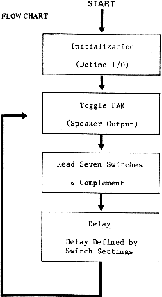
575.2 WRITING THE PROGRAM Having defined the interface for our application, we may proceed now to write our program. The effort proceeds in four stages: 1. Generate a flow chart 2. Generate assembly language code 3. Analyze the program 4. Generate machine language code
 58
58Briefly, our flow chart shows a first step of system initialization. During this step, we must define the I/O configuration of the system in that pin PA0 becomes the output to the speaker and that pins PA1 to PA7 become inputs from the seven switches. After initialization, a loop is set up which begins by inverting the state of PA0 (Toggle PA0). Next, the state of the switches is read and the data is complemented to produce the correct "sense" from the switches. The value so read is used to define a delay before returning to the start of the loop and again toggling the state of PA0. A little thought will show that this loop will produce a square wave with a frequency determined by the setting of the seven switches. Assembly Language Program Our next task is to convert the simple flow chart into a program. The program is first written in "Assembly Language". You should refer to your Programming Manual to become familiar with all of the pos- sible 6502 instructions (especially see Appendix B; Instruction Summary). Figure 5-2 shows the application example programmed in assembly language.
59
| | | | MACHINE | | | LABEL | OPCODE | OPERAND | CYCLES | COMMENTS | | INIT | LDA | #$01 | 2 | Define I/O 0=Input 1=Output | | | STA | PADD | 4 | PADD PORT A DATA DIRECTION REG. | | START | INC | PAD | 6 | Toggle PA0, PA1-PA7 Inputs | | | | | | not affected | | READ | LDA | PAD | 4 | READ switches into accumulator | | | EOR | #$FF | 2 | Complement switch value | | | LSR | A | 2 | Shift Accumulator 1 bit to right | | | TAX | | 2 | Transfer final count into X-Index | | DELAY | DEX | | 2 | Delay by an amount specified | | | BPL | DELAY | 3,2 | By the count in the X-Index | | | BMI | START | 3 | Go To START | | PADD | =$1701 | | | Define absolute address of | | | | | | Data Direction Reg. A | | PAD | =$1700 | | | Define absolute address of | | | | | | Data Reg. A |
Assembly Language Listing
FIGURE 5.2
60
You will note that each line of the program is broken into several fields: - A label field permitting you to assign a "name" to a specific location in the program. - An Operation Code field (Op Code) in which the exact instruction to be executed is defined. - An Operand Field where the exact data required by the instruction is defined together with certain symbols defining addressing modes or data formats. Symbols encountered generally in MOS Technology, Inc. manuals are: # Immediate Addressing $ Hex Code @ Octal Code % Binary Code ' ASCII literal = Equates a label to a value - A Machine Cycle field defining the total number of machine cycles required to execute an instruction. (This information is derived from Appendix B of the Programming Manual). - A Comment Field where the programmer may define the intent of specific program steps. Program Analysis The inclusion of the "machine cycle" information of the program chart (Figure 5-2) allows us to analyze the exact timing relationships involved in our program example. Note that the KIM-1 system operates from a fixed frequency (1 MHz) oscillator with each machine cycle being 1us. Therefore, an instruction like "INC PAD" which requires 6 machine cycles will be executed in a 6µs period.
61
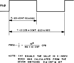
By counting the total machine cycles occurring between each toggle of PAØ, an equation for the square wave frequency can be developed. The actual frequency is determined by the position of the seven switches, the number of machine cycles between each toggle of PAØ, and the basic clock rate (1 MHz) of the KIM-1 system. Figure 5-3 shows the waveform of the PAØ square wave and the derived equations for computing the exact frequency.
 Square Wave Output
FIGURE 5.3
62
Square Wave Output
FIGURE 5.3
62Machine Language Coding Our next problem is to convert our assembly language program into a program written in "machine language". The quickest and most foolproof method for accomplishing this conversion is by using the MOS Technology, Inc. Assembler (available for use on the time share services of United Computing Systems, Inc.). If you choose not to use this method, you will need to convert your source program to machine code using "paper-and-pencil" techniques. You should proceed by constructing a table similar to that shown in Figure 5-4.
| | INSTRUCTION || SOURCE CODE |
| ADDRESS | BYTE 1 | BYTE 2 | BYTE 3 || LABEL OP CODE OPERAND |
| 0200 | A9 | 01 | || INIT LDA #$01 |
| 0202 | 8D | 01 | 17 || STA PADD |
| 0205 | EE | 17 | || START INC PAD |
| 0208 | AD | 17 | || READ LDA PAD |
| 020B | 49 | FF | || EOR #$FF |
| 020D | 4A | | || LSR A |
| 020E | AA | | || TAX |
| 020F | CA | | || DELAY DEX |
| 0210 | 10 | F0 | || BPL DELAY |
| 0212 | 30 | F1 | || BMI START |
| 0214 | | | || |
Machine Language Code Table
FIGURE 5.4
The source code contained in your assembly language program
(Figure 5-2) is entered into the table first. A column is provided to
allow you to define the specific address at which an instruction is
located. The Instruction column provides space for defining one, two,
or three byte instructions. (Please refer to Appendix B of the Program-
ming Manual or to your Programming Card for specific Op Codes).
63
As an example, the first source instruction is LDA #$01 which, when translated, means load the accumulator with the byte stored in the next program location (hex 01). This is the "immediate" addressing mode defined by the "#" symbol. The Op Code for LDA# is A9. This value is entered in the first column under the heading, Instruction. The next column contains the hex 01 value defined by the source state- ment. The initial address for the program is inserted in the "Address" column as 0200 (an arbitrary selection). The total instruction LDA #$01 now occupies address locations 0200 and 0201. The next available address is 0202 which is inserted in the "Address" column for the next source instruction. In this manner, you will proceed through all of the source statements decoding each and entering one, two, or three bytes of machine code as required in the "Instruction" column. The "Address" column will contain the address of the first byte of machine code (the Op Code) for each source statement. In cases where the operand of the source statement is a symbol, the address to which the symbol has been equated should be filled in as the proper machine code. For example, the source statement "INC PAD" requires the incrementing of data stored at a location "PAD" defined in our assembly programs to have the address: PAD = 1700. Therefore, the address 1700 is entered as the second and third bytes of the source statement "INC PAD". (See Figure 5-4). Note also that when entering an address, such as 1700, the low order byte (00) is entered first and immediately after the Op Code and the high order byte (17) is entered next as the third byte of the instruction. When dealing with branch instructions (BPL, BMI, etc.), you will need to calculate the exact value of the offset which may be either positive (branch forward) or negative (branch backward). You should refer to Section 4.1.1 of the Programming Manual to explore "Basic Concept of Relative Branching." As an example, the source statement "BMI START" (See Figures 5-2 and 5-4) requires a branch backward by (-15) locations to the address labelled "START" (from address 0213 backward to 0205 inclusive).
64
(The 2's complement of the -15 displacement is F1 HEX which you should insert at location 0212). Had the branch been to a forward location the positive value of the offset would be inserted rather than the 2's complement value. 5.3 ENTERING THE PROGRAM With the program now reduced to machine language code, you may enter the program address and data codes listed in Figure 5-4 following the procedures detailed in Section 2.4. The procedure for entering the program is as follows: Press Keys See On Display [AD] [0] [2] [0] [0] 0200 xx [DA] [A] [9] 0200 A9 [+] [0] [1] 0201 01 [+] [8] [D] 0202 8D [+] [0] [1] 0203 01 [+] [1] [7] 0204 17 [+] [E] [E] 0205 EE [+] [0] [0] 0206 00 [+] [1] [7] 0207 17 [+] [A] [D] 0208 AD [+] [0] [0] 0209 00 [+] [1] [7] 020A 17 [+] [4] [9] 020B 49 [+] [F] [F] 020C FF [+] [4] [A] 020D 4A [+] [A] [A] 020E AA [+] [C] [A] 020F CA [+] [1] [C] 0210 1C [+] [F] [D] 0211 FD [+] [3] [0] 0212 30 [+] [F] [1] 0213 F1
Key Sequences: Enter Program
FIGURE 5.5
65
5.4 EXECUTING THE PROGRAM With the program entered, you may proceed to program execution. First, if the NMI vector has not been defined previously, enter the vector as follows: Press Keys See Displayed [AD] [1] [7] [F] [A] 17FA xx [DA] [0] [0] 17FA 00 [+] [1] [C] 17fb 1C This procedure insures that the [ST] key will be effective in tenninating the program. Now, select the starting address of your program (0200) and begin execution as follows: Press Keys See Displayed [AD] [0] [2] [0] [0] 0200 xx [GO] (DARK) The program will now execute. If your seven selector switches all are open, you will probably hear no sound from the speaker because the square wave frequency is too high. If all selector switches are closed, you will hear in the speaker the lowest frequency that can be generated with the program as currently written. You may experiment with other combinations of switch settings to hear a variety of tones from the speaker. Depression of the [ST] key will cause the program execution to stop (the tone will terminate) and the KIM-1 display will relight. The display will show the address and data for the next instruction to be executed (probably 020F or 0210 since this is the delay loop where the program spends most of its running time).
66
5.5 PROGRAM DEBUGGING AND MODIFICATION If your program did not execute correctly, you would follow a debugging procedure involving the following steps: Step 1: List the Program First make sure you have entered the program steps correctly. Select the starting address ([AD] [0] [2] [0] [0]) and observe that the correct data (A9) is displayed. Now, using the [+] key, step through the remaining program locations check- ing for the correct data stored in each location. Step 2: Single Step the Program Follow the procedures listed in Section 5-4 for program execution but before depressing the [GO] key, place the SST slide switch in the ON position. Now, press the [GO] key and the first instruction will be executed. The display will relight indicating that the operating program is again in control of the system. The address displayed will be the address of the first byte of the next instruction to be executed. You may press the [GO] key again to execute the next instruction or you may choose to investigate changes in the contents of machine registers stored in selected memory locations (See Figure 3-13). The procedure detailed in Figure 5-6 gives a good indication of the various operations you may wish to perform in the SST mode. Step 3: Check the I/O Operations If program entry has been verified and program execution in the SST mode appears to be normal, you may wish to verify the correct operation of your specific I/O configuration. You should recall that writing to or reading from any I/O port is the same as reading from or writing to any other memory location in the system. Therefore, if you select the address of an I/O port, the KIM-1 display will show you the hex code for the data being read from that address and thus, directly indicate the state of each I/O pin in the port. For example, the
67
address of the I/O port used for your sample program is 1700. Press [AD] [1] [7] [0] [0] and the display will show the hex code corresponding to the settings of your selector switches. If you change the positions of your selector switches, you will see the hex code change in the data field of the display. Now, leave the same address (1700) selected and press the [DA] key. If you press any of the hex keys [0] to [F] you will write the data to the I/O port (1700). Since seven of the pins of this I/O port are defined as inputs, only one (PA0) will act as an output and will respond to the data entered by you from the keyboard. Try alternating rapidly between the [0] and [1] keys and you should hear clicking in the speaker indicating that you are successfully toggling the PA0 pin. This concept of using the KIM-1 keyboard and display to exercise and verify the operation of I/O ports is a generally useful technique for debugging the hardware portions of most specific applications.
68
Press Keys See On Display Comments [AD] [0] [2] [0] [0] 0200 A9 Select first instruction address | SST |X| |ON 0200 A9 Set SST to ON; All selector switches open [GO] 0202 8D Accumulator now loaded with $01 [GO] 0205 EE PADD now loaded [GO] 0208 AD PA0 now toggled [GO] 020B 49 Switch values (PA1-PA7) now [GO] loaded [GO] 020D 4A Accumulator now complemented [GO] 020E AA Accumulator now right shifted 1 Bit [AD] [0] [0] [F] [3] 00F3 xx Display Accu [+] 00F4 xx Display Y - INDEX [+] 00F5 00 Display X - INDEX [PC] 020E AA Restore PC (TAX will execute next) [GO] 020F CA Accumulator now loaded in X-INDEX [AD] [0] [0] [F] [3] 00F3 00 Display Accumulator [+] 00F4 xx Display Y-INDEX [+] 00F5 00 Display X-INDEX (A=0->X) [PC] 020F CA Restore PC [GO] 0210 10 DEX now completed [AD] [0] [0] [F] [5] 00F5 FF Display X-INDEX (X<0) [PC] 0210 10 Restore PC [GO] 0212 30 No branch (Result of DEX not positive) [GO] 0205 EE Branch (Result of DEX is negative). In earlier sections you have learned that the MCS 6502 Microprocessor Array is capable of directly addressing up to 65,536 locations (bytes) of memory. (Usually abbreviated to 65K where "1K" for the remainder of this section is to mean 1024 memory locations). In this section, we will discuss first the techniques for adding memory or I/O locations to the system and next, the proper handling of interrupt vectors in an expanded system. 6.1 MEMORY AND I/O EXPANSION In the KIM-1 system, the management of input/output data is handled exactly the same as transfers to or from any other memory location in the system. There are no instructions dealing specifically with input/output transfers. Instead, transfer of data is accomplished by reading from or writing to registers connected to the data bus and to I/O pins in specific I/O interface devices (such as the 6530 array). These registers have a specific address in the system just as does any other memory location. Therefore, when we speak of expanding the memory of the KIM-1 system, we are defining the methods for expanding both the real memory (RAM, ROM, PROM, etc.) as well as the I/O ports since they are both treated exactly alike as far as address assignments are concerned.
71
The first and most easilly implemented memory expansion is the addition of up to 4K of memory space. You will recall that the lowest 8K memory locations are defined by an address decoder included on the KIM-1 module, (Device U4 on the schematic). The eight outputs of this decoder (KØ to K7) each define a 1K block of addresses in the lowest 8K of the memory map. Three of the outputs (K5, K6, K7) are used to select ROM, RAM, I/O and Timer locations on the two 6530 arrays while a fourth (K0) is used to select the 1024 locations of the static RAM memory. The remaining four outputs (K1, K2, K3, K4) are not used on the KIM-1 module but instead, are brought out to the Expansion connector for use as chip selects for memory or I/O additions. Figure 6-1 shows the proper method for deriving the four chip select signals for the additional 4K of memory. Note that one of input pins of the decoder (D) was brought out to the Application Connector. It was this pin which we asked you to connect to ground in Chapter 2 of this manual. As long as this point remains connected to ground, the decoder will always select the lowest 8K addresses of the memory field regardless of the state of AB13, AB14, and AB15. If you wish to expand the memory and I/O address space beyond the lower 8K addresses, you must arrange to de-select the lower 8K memory block while selecting some other 8K block. One suggested method for expanding beyond the lower 8K space is shown in Figure 6-2. Note that the three high order address bits (AB13, AB14, AB15) are connected to a decoder. The eight outputs of the decoder act to divide the total 65K memory space into eight blocks of 8K each (8K0, 8K1, etc.). Now, the 8K0 output may be returned as the fourth inpur (D) to the de- coder (U4) on the KIM-1 module causing the proper selection and de-selec- tion of this block within the total address space. The remaining seven outputs (8K1 to 8K7) may be used to select and de-select the additional decoders shown in Figure 6-2. You need add only as many decoders (one for each 8K block of memory) as you need for your desired memory expansion.
72
A word of caution is in order when you decide to add memory to your system. You have noticed the inclusion of the line receivers for the AB10, AB11, and AB12 signals, (See Figure 6-2). These devices are included because of loading limitations placed on the address bus lines of the 6502 array (Each such line is capable of driving one standard TTL load and l3Opf of capacity. See Appendix G).
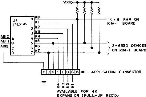 4K Expansion
FIGURE 6.1
73
4K Expansion
FIGURE 6.1
73
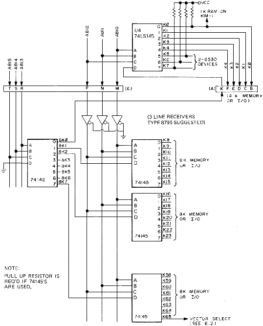 65K Expansion
FIGURE 6.2
74
65K Expansion
FIGURE 6.2
74Before deciding how to expand your system, we recommend a careful study of all of the loading limitations of the KIM-1 signals since almost certainly you will require additional buffering circuits if correct operation is to be achieved. 6.2 INTERRUPT VECTOR MANAGEMENT We have referred several times in earlier sections to the interrupt features of the 6502 Microprocessor Array. We suggest now a careful reading of Section 9 of the Programming Manual for the subject "Reset and Interrupt Considerations". In summary, there are three possible types of interrupt: Reset, NMI, and IRQ. Each will occur in response to an activation of one of the three pins of the 6502 array (RST, NMI, IRQ). In response to these inputs, the 6502 array will fetch the data stored at a specific pair of addresses and load the data fetched into the program counter. The addresses are hardware determined and not under the control of the programmer. The specific addresses for each type of interrupt are: FFFA, FFFB - NMI Vector FFFC, FFFD - RST Vector FFFE, FFFF - IRQ Vector You will note that these addresses define the highest six locations in the 65K memory map. In the KIM-1 system, three address bits (AB13, AB14, ABl5) are not decoded at all. Therefore, when the 6502 array generates a fetch from FFFC and FFFD in response to a RST input, these addresses will be read as 1FFC and 1FFD and the reset vector will be fetched from these locations. You now see that all interrupt vectors will be fetched from the top 6 locations of the lowest 8K block of memory which is the only memory block decoded for the unexpanded KIM-1 system.
75
It is typical in any system to store the interrupt vectors in ROM so that they are immediately available after power-on. However, it is desirable that for the NMI and IRQ interrupts, the programmer be allowed to define as a variable the exact vector to which these interrupts will direct the system. Accordingly, the NMI and IRQ vector locations contain an indirect jump instruction referencing a RAM location into which the programmer will store the specific vector for the two types of interrupt. In the KIM-1 system, locations 17FA and 17FB contain the actual NMI vector and 17FE with 17FF contain the actual IRQ vector. The RST vector is not handled in this manner and always directs the system to the first step of the power-on initialization routine. But what happens if we expand our memory above the lowest 8K block included in the KIM-1 system? Recall that we now must use ABl3, ABT4, and AB15 to decode the additional address locations of the memory. By so doing, the interrupt vector locations are no longer located in the K7 memory block since the decoder (U4) is de-selected in response to the addresses generated by the 6502 array in fetching the interrupt vectors (FFFA for example). We would have the same problem even in an unexpanded system if we wished to use a RST vector and initialization routine different than what the KIM-1 system provides and if the RST vector was to be located in a 1K block lower than K7 (K0 for instance). The solution to this dilemma is to generate logically a special signal for interrupt select. Referring to Figure 6-2, a special signal called "Vector Select" is created to define the highest 1K memory black (K65). The fetch of any interrupt vector will cause this signal to go low "Select". Assuming that the K65 state is not used to select RAM, this signal may be "wire-or'd" with any one of the other "K" signals (K0 to K64) to define exactly which 1K block is to contain the interrupt vectors.
76
As an example, assume that you have connected the K65 "Vector Select" line to the K0 line. When a RST occurs, the 6502 array generates a fetch from locations FFFC and FFFD. These addresses cause K65 to be selected which, in turn, accesses the K0 field of the memory and causes the actual fetch of the RST vector from locations 03FC and 03FD. (Had you chosen to connect K65 to K7, the fetch of the reset vectors would occur from locations 1FFC and 1FFD). In this way, the highest six addresses of any 1K block of memory may be used to supply the interrupt vectors for the system. If desired, a switch could be installed to allow you to select different areas of memory as the source locations for the interrupt vectors. (By the way, we selected the 75145 type decoders in Figure 6-2 specifically to allow the "wire-or" of K65 with any other K. This is possible because the 75145 decoder is provided with open-collector outputs which allows "wire-or" of several states using an external load resistor.) An even simpler arrangement using the "Vector Select" approach is shown in Figure 6-3. Here, the KIM-1 system is assumed to have only the lower 8K of memory in place. The address decoder (U4) is de-selected using the AB15 signal which becomes "true" whenever an interrupt vector fetch is initiated by the system. The same signal (AB15) is inverted and "wire-or'd" through a switch to the K0 or the K7 chip select lines. Now, depending upon the position of the switch, interrupt vectors will be fetched from the top 6 addresses of either block K0 or K7. K0 in the KIM-1 system is the RAM and K7 is the ROM in the 6530-002 array (the operating program). In this way, you may have two different sets of inter- rupt vectors in your system and may select which set is to be used with a simple switch.
77
Should you experience difficulty with your KIM-1 module and be unable to diagnose or correct the problem, you may return the unit to MOS Technology, Inc. for repair. 7.1 IN-WARRANTY SERVICE All KIM-1 series Microcomputer Modules are warranted by MOS Technology, Inc. against defects in workmanship and materials for a period of ninety (90) days from date of delivery. During the warranty period, MOS Technology, Inc. will repair or, at its option, replace at no charge components that prove to be defective provided that the module is returned, shipping prepaid, to: KIM Customer Service Department MOS Technology, Inc. 950 Rittenhouse Road Norristown, Pennsylvania 19401 This warranty does not apply if the module has been damaged by accident or misuse, or as a result of repairs or modifications made by other than authorized personnel at the above captioned service facility No other warranty is expressed or implied. NOS Technology, Inc. is not liable for consequential damages.
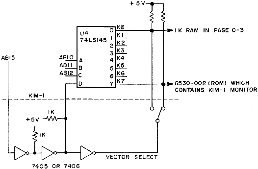 Vector Selection
FIGURE 6.3
78
Vector Selection
FIGURE 6.3
78
79
7.2 OUT-OF-WARRANTY SERVICE Beyond the ninety (90) day warranty period, KIM modules will be repaired for a reasonable service fee. All service work performed by MOS Technology, Inc. beyond the warranty period is warranted for an additional ninety (90) day period after shipment of the repaired module. 7.3 POLICY ON CHANGES All KIM series modules are sold on the basis of descriptive specifications in effect at the time of sale. MOS Technology, Inc. shall have no obligation to modify or update products once sold. MOS Technology, Inc. reserves the right to make periodic changes or improvements to any KIM series module. 7.4 SHIPPING INSTRUCTIONS It is the customer's responsibility to return the KIM series module with shipping charges prepaid to the above captioned service facility. For in-warranty service, the KIM module will be returned to the customer, shipping prepaid, by the fastest economical carrier. For out-of-warranty service, the customer will pay for shipping charges both ways. The repaired KIM module will be returned to the customer C.O.D. unless the repairs and shipping charges are prepaid by the customer. Please be certain that your KIM module is safely packaged when returning it to the above captioned service facility.
80
APPENDIX A
| | | | |
| ITEM | PART | QTY. | DESCRIPTION |
| | | | |
| 1. | Ul | 1 | 6502 Microprocessor |
| 2. | U2 | 1 | 6530 ROM RAM I/O Chip-02 |
| 3. | U3 | 1 | 6530 ROM RAM I/O Chip-03 |
| 4. | U5 through U12 | 8 | 6102 RAM 500ns Acc,0ns |
| 5. | U18 through U23 | 6 | 7 SEG .3" Red Display |
| 6. | U25 | 1 | 556 Timer IC |
| 7. | U27 | 1 | 565 Phase Lock Loop |
| 8. | U28 | 1 | 311 Comparator |
| 9. | U24 | 1 | 74145 BCD Decoder IC |
| 10. | U13 & U14 | 2 | 74125 TRI STATE Buffer |
| 11. | u15 | 1 | 7400 Quad Nand IC |
| 12. | U16 | 1 | 7404 Hex Inverter IC |
| 13. | U17 | 1 | 7406 Hex Inv. O/C IC |
| 14. | U26 | 1 | 7438 Quad Nand O/C IC |
| 15. | CR1,2,3,4,&8 | 5 | 20 mA. 50v Diode - 1N914 |
| 16. | CR5, CR6 | 2 | 1A 50v Diode - 1N4001 |
| 17. | CR7 | 1 | 6.2v ½w Z. Diode - 1N4735 |
| 18. | Q7 | 1 | NPN Transistor B>20, VCE>12 - 2N5371 |
| 19. | Q1 through Q6 | 6 | PNP Transistor B>20, VCE>6 - 2N5375 |
| 20. | 04 & 05 | 2 | 47K ±10% ¼w Resistor |
| 21. | R1,2,3,4, & 6 | 5 | 3.3K ±10% ¼w Resistor |
| 22. | R34 & P50 | 2 | 2.2K ±10% ¼w Resistor |
| 23. | Rl2-R17, R41-R46 | 12 | l.0K ±10% ¼w Resistor |
| 24. | R35 through R40 | 6 | 560Ohm ±10% ¼w Resistor |
| 25. | R18-R23, R47 | 7 | 220Ohm ±10% ¼w Resistor |
| 26. | R33 | 1 | 47Ohm ±l0% ¼w Resistor |
| 27. | R52 | 1 | 5 Meg. ±10% ¼w Resistor |
| 28. | R51 | 1 | 30K ±5% ¼w Resistor |
| 29. | R7,R8,R9,R10&R1l | 5 | l0K ±5% 1/4w Resistor |
| 30. | R48, R49 | 2 | 150 ±5% 0 |
| 31. | R26 through R32 | 7 | 82Ohm ±05% |
| 32. | VR1 | 1 | 5K Potentiometer |
| 33. | C2, C3, C6 | 3 | .22±10% uf.>12 wv. cap |
| 34. | C1, C4 | 2 | 1uf+80-l0%>12WV Cap |
| 35. | CS | 1 | .33 uf±l0%>12WV Cap |
| 36. | C7,C8,C15,C16,C17 | 5 | .1uf+80-l0%>12WV Cap |
| 37 | C9, C10, C11 | 3 | .0068uf±l0%>l2WV |
| 38. | C12 | 1 | .047uf±1O%>l2WV |
| 39. | C13 | 1 | .022uf±10%>l2WV |
| 40. | C14 | 1 | .OOluf±lO%>l2WV |
| 41. | | 1 | 44 Pin Edge Conn. (Vector #R644) |
| 42. | X1 | 1 | 1 MHz XTAL |
| 43. | | 1 | PCB. |
| 44. | | 1 | 24 Key KBD |
| 45. | | 6 | Rubber Pads |
| 46. | | 1 | Shipping Bag (Static Free) |
| 47. | | 1 | Shipping Box |
| 48. | | 1 | Hardware Manual |
| 49. | | 1 | Software Manual |
| 50. | | 1 | KIM Manual |
| 51. | | 1 | Warranty Card |
| 52. | | 1 | Wall Chart |
| 53. | | 2 | #2 x ¼ SS Screws (Keyboard) |
| 54. | | 1 | Program Card |
| 55. | C18 | 1 | 10pf CAP |
| 56. | R53 | 1 | 330K ¼w Resistor |
| 57. | U4 | 1 | 74L5145 BCD Decoder lC |
SYMPTOM: Display Not Lit
1. Test +5 volt power supply. Using a VOM check for +5
volts between Pin E-21 and E-22. Also check for +5
volts between Pin A-A and Pin A-1. KIM-1 power supply
should be set at +5v ñ 5%.
2. Test KB/TTY option wiring (Figure 2-4). Pin A-21 should
not be connected to Pin A-V.
3. Make sure decoder is enabled. See Figure 2-2 and insure
that Pin A-K is connected to ground.
4. Depress the reset key and check all other keys to insure
that no key is stuck.
5. Place a VOM between Pin E-21 (+5v) and Pin E-7 (Reset).
Alternately depress and release the reset key checking to
see if the voltage swings from (>4v) to (<1v).
6. Test Pin E-V (è2) with an oscilloscope and insure 1 MHz
operation.
SYMPTOM: Cannot Dump to Audio Tape
Cannot Load From Audio Tape
1. Test +12 volt power supply. Using a VOM check for +12
volts between Pin A-N (+12v) and Pin A-1 (GND). Set
power supply to +12v ñ 5%. (See Figure 2-2).
2. Check volume control on the tape recorder (Set at half
way point).
APPENDIX A
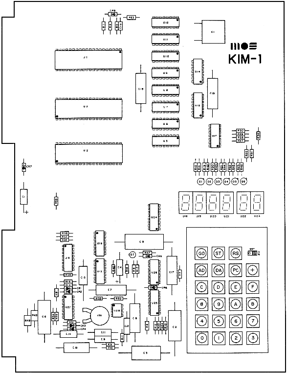 B-1
B-1
C-1
3. Make sure that you are using the proper tape output pin. See Figure 2-3. 4. Check the tape interface circuit by disconnecting the tape recorder and shorting Pin A-P (Audio Out High) to Pin A-L (Audio In). Set up KIM-1 monitor to dump a section of memory. Using an oscilloscope observe data at Pin E-X (PLL TEST). See Appendix E for correct data format and calibration procedure. 5. Record voice on a section of tape and play it back to insure that the tape recorder is working. Connect another tape recorder to the system or try another cassette. 6. Make sure Status Register (Location 00F1) has been loaded with data value "00". 7. Make sure Tone Control is set to High. SYMPTOM: TTY Interface Problems 1. Make sure that Pin A-21 is connected to Pin A-V (Figure 2-4) to allow TTY operation. 2. Compare the connections on Figure 2-4 with interface schematics in your TTY manual ( or any other serial teleprinter ). 3. Depress the reset key on the KIM-1 keyboard followed by a rub out character from the TTY. Data is stored out onto your audio cassette recorder in a specific format designed to insure an error free recovery. In the unlikely event that a playback error does occur, several "ERROR DETECTION" methods are incorporated to warn you of this condition. Data is transmitted to the tape recorder in the form of serial "ASCII" encoded characters (seven data bits plus Parity bit). Data retrieved from the memory is converted into this form by separating each byte into two half bytes. The half bytes are then converted into their ASCII equivalents. Each record transmitted begins with a leader of one hundred "SYN" characters (ASCII 16) followed by a * character (ASCII 2A). During playback, this pattern allows your micro-computer to detect the start of a valid data record and synchronize to the serial data stream. Following the *, the record identification number (ID), and starting address low (SAL) and the starting address high (SMI) are transmitted. The data specified by the starting (SAL, SAH) and ending limits (EAL, EAH) is transmitted next followed by a "/" character (ASCII 2F) to indicate the end of the data portion of the record. Following the "/" two "CHECK-SUM" bytes are transmitted for comparison with a calculated check-sum number during playback to further insure that a proper data retrieval has taken place. Two "EOT" characters (ASCII ø4) mark the end of record transmission.
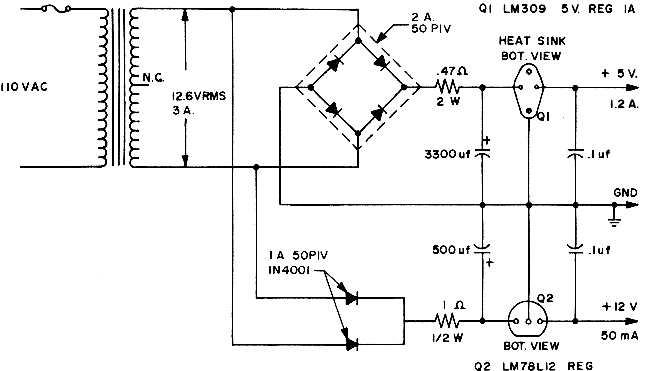 Suggested Power Supply
D-1
Suggested Power Supply
D-1
E-1
Each transmitted bit begins with a 3700 hertz tone and ends with a 2400 hertz tone. "Ones" have the high to low frequency transition at one-third of the bit period. "Zeros" have the transition at two- thirds of the period. During playback the 565 phase locked loop locks to, and tracks these two frequencies producing (through the 311 comparator) a logic "1" pulse of one-third the bit period for a "One". A pulse two thirds the bit period is likewise produced for a "Zero". Your microcomputer uses a software controlled algorithm for converting this signal into eight bit data words. The frequency shift keyed phase lock loop method of data recovery is relatively insensitive to amplitude and phase variations. The "FREE RUNNING" frequency of the phase lock loop has been adjusted at the factory to a frequency half way between the two data frequencies (called the Center Frequency). This adjustment is accomplished by strapping Pin A-P (Audio Out High) to Pin A-L (Audio In). A program starting at address 1A6BHEX provides the center frequency reference that allows the loop to be adjusted by potentiometer VR1. Pin E-X (PLL TEST) is monitored with a voltmeter while the pot is rotated until the voltmeter reading is at the transition point between a logical "1" (+5v) and "0" (GND). THIS ADJUSTMENT HAS BEEN FACTORY PRESET AND SHOULD ONLY REQUIRE ADJUSTMENT DUE TO COMPONENT REPLACE0NT.' The paper tape LOAD and DUMP routines store and retrieve data in a specific format designed to insure error free recovery. Each byte of data to be stored is converted to two half bytes. The half bytes (whose possible values are 0 to FHEX) are translated into their ASCII equivalents and written out onto paper tape in this form. Each record outputted begins with a ";" character (ASCII 3B) to mark the start of a valid record. The next byte transmitted (18HEX) or (2410) is the number of data bytes contained in the record. The record's starting address High (1 byte, 2 characters), starting address Lo (1 byte, 2 characters), and data (24 bytes, 48 characters) follow. Each record is terminated by the record's check-sum (2 bytes, 4 characters), a carriage return (ASCII OD), line feed (ASCII øA), and six "NULL" characters (ASCII øø). The last record transmitted has zero data bytes (indicated by ;00) The starting address field is replaced by a four digit Hex number repre- senting the total number of data records contained in the transmission, followed by the records usual check-sum digits. A "XOFF" character ends the transmission. ;180000FFEEDDCCBBAA0099887766554433221122334455667788990AFC ;0000010001
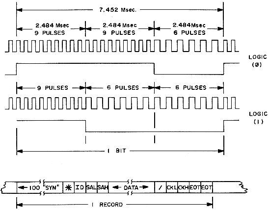 Audio Tape Format
FIGURE E-1
E-3
Audio Tape Format
FIGURE E-1
E-3
F-1
During a "LOAD" all incoming data is ignored until a ";" character is received. The receipt of non ASCII data or a mismatch between a records calculated check-sum and the check-sum read from tape will cause an error condition to be recognized by KIM. The check-sum is calculated by adding all data in the record except the ";" character. The paper tape format described is compatible with all other MOS Technology, Inc. software support programs.
F-2
APPENDIX G 6502 CHARACTERISTICS
Clocks (ø1, ø2)
The MCS 6502 is supplied with an internal clock generator. The
frequency of this clock is crystal controlled.
Address Bus (A0-A15)
These outputs are TTL compatible, capable of driving one standard
TTL load and 13Opf.
Data Bus (D0-D7)
Eight pins are used for the data bus. This is a bi-directional bus,
transferring data to and from the device and peripherals. The
outputs are tri-state buffers capable of driving one standard
TTL load and 130pf.
Ready (RDY)
This input signal allows the user to single cycle the microprocessor
on all cycles except write cycles. A negative transition to the low
state during or coincident with phase one (þ1) will halt the micro-
processor with the output address lines reflecting the current
address being fetched. This condition will remain through a
subsequent phase two (þ2) in which the Ready signal is high. This
feature allows microprocessor interfacing with low speed PROMS as
well as fast (max 2 cycle) Direct Memory Access (DMA). If Ready
is low during a write cycle, it is ignored until the following
read operation.
APPENDIX G 6502 CHARACTERISTICS
G-1
Interrupt Request (IRQ) This TTL level input requests that an interrupt sequence begin within the microprocessor. The microprocessor will complete the current instruction being executed before recognizing the request. At that time, the interrupt mask bit in the Status Code Register will be examined. If the interrupt mask flag is not set, the microprocessor will begin an interrupt sequence. The Program Counter and Processor Status Register are stored in the stack. The microprocessor will then set the interrupt mask flag high so that no further interrupts may occur. At the end of this cycle, the program counter low will be loaded from address FFFE, and program counter high from location FFFF, therefore trans- ferring program control to the memory vector located at these addresses. The RDY signal must be in the high state(for control to the memory vector) located at these addresses. The RDY signal must be in the high state for any interrupt to be recognized. A 3Kþ external register should be used for proper wire-OR operation. Non-Maskable Interrupt (NMI) A negative going edge on this input requests that a non-maskable interrupt sequence be generated within the microprocessor. NMI is an unconditional interrupt. Following completion of the current instruction, the sequence of operations defined for IRQ will be performed, regardless of the state of the interrupt mask flag. The vector address loaded into the program counter, low and high, are locations FFFA and FFFB respectively. The instructions loaded at these locations causes the microprocessor to branch to a non-maskable interrupt routine in memory. NMI also requires an external 3KOhm resistor to Vcc for proper wire-OR operations.
G-2
Inputs IRQ and NMI are hardware interrupts lines that are sampled during ø2 (phase 2) and will begin the appropriate interrupt routine on the ø1 (phase 1) following the completion of the current instruction. Set Overflow Flag (S.O.) This TTL level input signal allows external control of the overflow bit in the Status Code Register. SYNC This output line is provided to identify those cycles in which the microprocessor is doing an Op Code fetch. The SYNC line goes high during ø1 of an Op Code fetch and stays high for the remainder of that cycle. If the RDY line is pulled low during the þ1 clock pulse in which SYNC went high, the processor will stop in its current state and will remain in the state until the RDY line goes high. In this manner, the SYNC signal can be used to control RDY to cause single instruction execution. RESET This input is used to reset or start the microprocessor from a power down condition. During the time that this line is held low, writing to or from the microprocessor is inhibited. When a positive edge is detected on the input, the microprocessor will immediately begin the reset sequence. After a system initialization time of six clock cycles, the mask interrupt flag will be set and the microprocessor will load the program counter from the memory vector locations FFFC and FFFD. This is the start location for program control. After Vcc reaches 4.75 volts in a power up routine, reset must be held low for at least two clock cycles. When the reset signal goes high following these two clock cycles, the microprocessor will proceed with the normal reset procedure detailed above.
G-3
APPENDIX H 6530 CHARACTERISTICS
The MCS 6530 is designed to operate in conjunction with the MCS 650X
Microprocessor Family. It is comprised of a mask programmable 1024 x 8
ROM, a 64 x 8 static RAM, two software controlled 8 bit bi-directional
data ports allowing direct interfacing between the microprocessor unit
and peripheral devices, and a software programmable interval timer
with interrupt, capable of timing in various intervals from 1 to 262,144
clock periods.
APPENDIX H 6530 CHARACTERISTICS
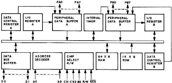 MCS 6530 Block Diagram
FIGURE H.1
H-1
MCS 6530 Block Diagram
FIGURE H.1
H-1Reset (RES) During system initialization a Logic "0" on the RES input will cause a zeroing of all four I/O registers. This in turn will cause all I/O buses to act as inputs thus protecting external components from possible damage and erroneous data while the system is being configured under software control. The Data Bus Buffers are put into an OFF-STATE during Reset. Interrupt capability is disabled with the RES signal. The RES signal must be held low for at least one clock period when reset is required. Input Clock The input clock is a system Phase Two clock which can be either a low level clock (VIL < 0.4, VIH > 2.4) or high level clock (VIL < 0.2, VIH = Vcc +.3/-.2) Read/Write (R/W) The R/W signal is supplied by the microprocessor array and is used to control the transfer of data to and from the microprocessor array and the MCS 6530. A high on the R/W pin allows the processor to read (with proper addressing) the data supplied by the MCS 6530. A low on the R/W pin allows a write (with proper addressing) to the MCS 6530. Interrupt Request (IRQ) The IRQ pin is an interrupt pin from the interval timer. This same pin, if not used as an interrupt, can be used as a peripheral I/O pin (PB7). Then used as an interrupt, the pin should be set up as an input by the data direction register. The pin will be normally high with a low indicating an interrupt from the MCS 6530.
H-2
Data Bus (D0-D7) The MCS 6530 has eight bi-directional data pins (Dø-D7). These pins connect to the system's data lines to allow transfer of data to and from the microprocessor array. The output buffers remain in the off state except when a Read operation occurs. Peripheral Data Ports The MCS 6530-002, MCS 6530-003 both have 15 pins available for peripheral I/O operations. Each pin is individually software programmable to act as either an input or an output. The 15 pins are divided into 2 8-bit ports, PAø-PA7 and PBø-PB7. PB6 was used as a chip select and is not available to the user. The pins are set up as an input by writing a "0" into the corresponding bit of the data direction register. A "1" into the data direction register will cause its corresponding bit to be an output. Wben in the input mode, the peripheral output buffers are in the "1" state and a pull-up device acts as less than one TTL load to the peripheral data lines. On a Read operation, the microprocessor unit reads the peripheral pin. When the peripheral device gets information from the MCS 6530 it receives data stored in the data register. The microprocessor will read correct information if the peripheral lines are greater than 2.0 volts for a "1" and less than 0.8 volts for a "0" as the peripheral pins are all TTL compatible. Pins PA0 and PB0 are also capable of sourcing 3 ma at 1.5v, thus making them capable of Darlington drive. Pin PB7 has no internal pull-up (to allow collector-oring with other devices). Address Lines (Aø-A9) There are 10 address pins. In addition to these 10, there is the ROM SELECT pin. The above pins, Aø-A9 and ROM SELECT, are always used as addressing pins. There are 2 additional pins which are mask programmable and can be used either individually or together as CHIP SELECTS. They are pins PB5 and PB6. When used as peripheral data pins they cannot be used as chip selects. PB5 was used as a data pin while PB6 was used as a chip select and is not available to the user.
H-3
A block diagram of the internal architecture is shown in Figure H-1 The NCS 6530 is divided into four basic sections, RAM, ROM, I/O and TIMER. The RAM and ROM interface directly with the microprocessor through the system data bus and address lines. The I/O section consists of 2 8-bit halves. Each half contains a Data Direction Register (DDR) and an I/O Register. ROM 1K Byte (8K Bits) The 8K ROM is in a 1024 x 8 configuration. Address lines A0-A9, as well as RSO are needed to address the entire ROM. With the addition of CS1 and CS2, seven NCS 6530's may be addressed, giving 7168 x 8 bits of contiguous ROM. RAM 64 Bytes (512 Bits) A 64 x 8 static RAM is contained on the MCS 6530. It is addressed by Aø-A5 (Byte Select), RSø, A6, A7, A8, A9 and CS1. Internal Peripheral Registers There are four internal registers, two data direction registers and two peripheral I/O data registers. The two data direction registers (A side and B side) control the direction of the data into and out of the peripheral pins. A "1" written into the Data Direction Register sets up the corresponding peripheral buffer pin as an output. Therefore, anything then written into the I/O Register will appear on that corresponding peripheral pin. A "0" written into the DDR inhibits the output buffer from transmitting data to or from the I/O Register. For example, a "1" loaded into data direction register A, position 3, sets up peripheral pin PA3 as an output. If a "0" had been loaded, PA3 would be configured as an input and remain in the high state. The two data I/O registers are used to latch data from the Data Bus during a Write operation until the peripheral device can read the data supplied by the microprocessor array.
H-4
During a read operation the microprocessor is not reading the I/O Registers but in fact is reading the peripheral data pins. For the peripheral data pins which are programmed as outputs the microprocessor will read the corresponding data bits of the I/O Register. The only way the I/O Register data can be changed is by a microprocessor Write operation. The I/O Register is not affected by a Read of the data on the peripheral pins. Interval Timer 1. Capabilities The KIM-1 Interval Timer allows the user to specify a preset count of up to 25610 and a clock divide rate of 1, 8, 64 or 1024 by writing to a memory location. As soon as the write occurs, counting at the specified rate begins. The timer counts down at the clock frequency divided by the divide rate. The current timer count may be read at any time. At the user's option, the timer may be programmed to generate an interrupt when the counter counts down past zero. When a count of zero is passed, the divide rate is automatically set to 1 and the counter continues to count down at the clock rate starting at a count of FF (-1 in two's complement arithmetic). This allows the user to determine how many clock cycles have passed since the timer reached a count of zero. Since the counter never stops, continued counting down will reach 00 again, then FF, and the count will continue. 2. Operation a. Loading the timer The divide rate and interrupt option enable/disable are programmed by decoding the least significant address bits. The starting count for the timer is determined by the value written to that address.
H-5
Writing to Address Sets Divide Ratio To Interrupt Capability Is 1704 1 Disabled 1705 8 Disabled 1706 64 Disabled 1707 1024 Disabled 170C 1 Enabled 170D 8 Enabled 170E 64 Enabled 170F 1024 Enabled b. Determining the timer status After timing has begun, reading address location 1707 will provide the timer status. If the counter has passed the count of zero, bit 7 will be set to 1, otherwise, bit 7 (and all other bits in location 1707) will be zero. This allows a program to "watch" location 1707 and determine when the timer has timed out. c. Reading the count in the timer If the timer has not counted past zero, reading location 1706 will provide the current timer count and disable the interrupt option; reading location 170E will provide the current timer count and enable the interrupt option. Thus the interrupt option can be changed while the timer is counting down. If the timer has counted past zero, reading either memory location 1706 or 170E will restore the divide ratio to its previously programmed value, disable the interrupt option and leave the timer with its current count (not the count originally written to the timer). Because the timer never stops counting, the timer will continue to decrement, pass zero, set the divide rate to 1, and continue to count down at the clock frequency, unless new information is written to the timer.
H-6
d. Using the interrupt option In order to use the interrupt option described above, line PB7 (application connector, pin 15) should be connected to either the IRQ (Expansion Connector, pin 4) or NMI (Expansion Connector, pin 6) pin depending on the desired interrupt function. PB7 should be programmed as in input line (it's normal state after a RESET). NOTE: If the programmer desires to use PB7 as a normal I/O line, the programmer is responsible for disabling the timer interrupt option (by writing or reading address 1706) so that it does not interfere with normal operation of PB7. Also, PB7 was designed to be wire-ORed with other possible interrupt sources; if this is not desired, a 5.1K resistor should be used as a pull-up from PB7 to +5v. (The pull-up should NOT be used if PB7 is connected to NMI or IRQ.)
PAGE 2
CARD # LOC CODE CARD
3 ; 666666 555555 333333 000000
4 ; 6 5 3 0 0
5 ; 6 5 3 0 0
6 ; 666666 555555 333333 0 0
7 ; 6 6 5 3 0 0
8 ; 6 6 5 3 0 0
9 ; 666666 666666 666666 000000
10 ;
11 ;
12 ;
13 ; 000000 000000 333333
14 ; 0 0 0 0 3
15 ; ------ 0 0 0 0 3
16 ; ------ 0 0 0 0 333333
17 ; ------ 0 0 0 0 3
18 ; 0 0 0 0 3
19 ; 000000 000000 333333
20 ;
21 ;
22 ;
23 ;
24 ;
25 ; COPYRIGHT
26 ; MOS TECHNOLOGY, INC
27 ; DATE: OCT 18, 1975 REV-D
28 ;
29 ;
30 ;
31 ; 6530-003 I.C. IS AN AUDIO CASSETT TAPE
32 ; RECORDER ENTENSION OF THE BASIC
33 ; KIM MONITOR
34 ;
35 ; IT FEATURES TWO BASIC ROUTINES
36 ; LOADT-LOAD MEM FROM AUDIO TAPE
37 ; DUMPT-STOR MEM ONTO AUDIO TAPE
38 ;
39 ; LOADT
40 ; ID=00 IGNORE ID
41 ; ID=FF IGN. ID USE SA FOR START ADDR
42 ; ID=01-FE IGN.ID USE ADDRESS ON TAPE
43 ;
44 ; DUMPT
45 ; ID=00 SHOULD NOT BE USED
46 ; ID=FF SHOULD NOT BE USED
47 ; ID=01-FE NORMAL ID RANGE
48 ; SAL LSB STARTING ADDRESS OF PROGRAM
49 ; SAH MSB
50 ; EAL ENDING ADDRESS OF PROGRAM
51 ; EAH MSB
52 ;
PAGE 3
CARD # LOC CODE CARD
54 ;
55 ; EQUATES
56 ; SET UP FOR 6530-002 I/O
57 ;
58 SAD =$1740 6530 A DATA
59 PADD =$1741 6530 A DATA DIRECTION
60 SBD =$1742 6530 B DATA
61 PBDD =$1743 6530 B DATA DIRECTION
62 CLK1T =$1744 DIV BY 1 TIME
63 CLK8T =$1745 DIV BY 8 TIME
64 CLK64T =$1746 DIV BY 64 TIME
65 CLKKT =$1747 DIV BY 1024 TIME
66 CLKRDI =$1747 READ TIME OUT BIT
67 CLKRDT =$1746 READ TIME
68 ;
69 0000 *=$00EF
70 ; MPU REG. SAVX AREA IN PAGE 0
71 ;
72 00EF PCL *=*+1 PROGRAM CNT LOW
73 00F0 PCH *=*+1 PROGRAM CNT HI
74 00F1 PREG *=*+1 CURRENT STATUS REG
75 00F2 SPUSER *=*+1 CURRENT STACK POINTER
76 00F3 ACC *=*+1 ACCUMULATOR
77 00F4 YREG *=*+1 Y INDEX
78 00F5 XREG *=*+1 X INDEX
79 ;
80 ; KIM FIXED AREA IN PAGE 0
81 ;
82 00F6 CHKHI *=*+1
83 00F7 CHKSUM *=*+1
84 00F8 INL *=*+1 INPUT BUFFER
85 00F9 INH *=*+1 INPUT BUFFER
86 00FA POINTL *=*+1 LSB OF OPEN CELL
87 00FB POINTH *=*+1 MSB OF OPEN CELL
88 00FC TEMP *=*+1
89 00FD TMPX *=*+1
90 00FE CHAR *=*+1
91 00FF MODE *=*+1
92 ;
93 ; KIM FIXED AREA IN PAGE 23
94 ;
95 0100 *=$17E7
96 17E7 CHKL *=*+1
97 17E8 CHKH *=*+1 CHKSUM
98 17E9 SAVX *=*+3
99 17EC VEB *=*+6 VOLATILE EXECUTION BLOCK
100 17F2 CNTL30 *=*+1 TTY DELAY
101 17F3 CNTH30 *=*+1 TTY DELAY
102 17F4 TIMH *=*+1
103 17F5 SAL *=*+1 LOW STARTING ADDRESS
104 17F6 SAH *=*+1 HI STARTING ADDRESS
105 17F7 EAL *=*+1 LOW ENDING ADDRESS
PAGE 4
CARD # LOC CODE CARD
106 17F8 EAH *=*+1 HI ENDING ADDRESS
107 17F9 ID *=*+1 TAPE PROGRAM ID NUMBER
108 ;
109 ; INTERRUPT VECTORS
110 ;
111 17FA NMIV *=*+2 STOP VECTOR (STOP=1C00)
112 17FC RSTV *=*+2 RST VECTOR
113 17FE IRQV *=*+2 IRQ VECTOR (BRK= 1C00)
114 ;
PAGE 5
CARD # LOC CODE CARD
116 1800 *=$1800
117 ;
118 ; INIT VOLATILE EXECUTION BLOCK
119 ; DUMP MEM TO TAPE
120 ;
121 1800 A9 AD DUMPT LDA #$AD LOAD ABSOLUTE INST
122 1802 8D EC 17 STA VEB
123 1805 20 32 19 JSR INTVEB
124 ;
125 1808 A9 27 LDA #$27 TURN OFF DATAIN PB5
126 180A 8D 42 17 STA SBD
127 180D A9 BF LDA #$BF CONVERT PB7 TO OUTPUT
128 180F 8D 43 17 STA PBDD
129 ;
130 1812 A2 64 LDX #$64 100 CHARS
131 1814 A9 16 DUMPT1 LDA #$16 SYNC CHAR'S
132 1816 20 7A 19 JSR OUTCHT
133 1819 CA DEX
134 181A D0 F8 BNE DUMPT1
135 ;
136
137 181C A9 2A LDA #$2A START CHAR
138 181E 20 7A 19 JSR OUTCHT
139 ;
140 1821 AD F9 17 LDA ID OUTPUT ID
141 1824 20 61 19 JSR OUTBT
142 ;
143 1827 AD F5 17 LDA SAL OUTPUT STARTING
144 182A 20 5E 19 JSR OUTBTC ADDRESS
145 182D AD F6 17 LDA SAH
146 1830 20 5E 19 JSR OUTBTC
147 ;
148 1833 AD ED 17 DUMPT2 LDA VEB+1 CHECK FOR LAST
149 1836 CD F7 17 CMP EAL DATA BYTE
150 1839 AD EE 17 LDA VEB+2
151 183C ED F8 17 SBC EAH
152 183F 90 24 BCC DUMPT4
153 ;
154 1841 A9 2F LDA #'/ OUTPUT END OF DATA CHAR
155 1843 20 7A 19 JSR OUTCHT
156 1846 AD E7 17 LDA CHKL LAST BYTE HAS BEEN
157 1849 20 61 19 JSR OUTBT OUTPUT NOW OUTPUT
158 184C AD E8 17 LDA CHKH CHKSUM
159 184F 20 61 19 JSR OUTBT
160 ;
161 ;
162 1852 A2 02 LDX #$02 2 CHAR'S
163 1854 A9 04 DUMPT3 LDA #$04 EOT CHAR
164 1856 20 7A 19 JSR OUTCHT
165 1859 CA DEX
166 185A D0 F8 BNE DUMPT3
167 ;
PAGE 6
CARD # LOC CODE CARD
168 185C A9 00 LDA #$00 DISPLAY 0000
169 185E 85 FA STA POINTL FOR NORMAL EXIT
170 1860 85 FB STA POINTH
171 1862 4C 4F 1C JMP START
172 ;
173 1865 20 EC 17 DUMPT4 JSR VEB DATA BYTE OUTPUT
174 1868 20 5E 19 JSR OUTBTC
175 ;
176 186B 20 EA 19 JSR INCVEB
177 186E 4C 33 18 JMP DUMPT2
178 ;
179 ; LOAD MEMORY FROM TAPE
180 ;
181 ;
182 1871 0F 19 TAB .WORD LOAD12
183 1873 A9 8D LOADT LDA #$8D INIT VOLATILE EXECUTION
184 1875 8D EC 17 STA VEB BLOCK WITH STA ABS.
185 1878 20 32 19 JSR INTVEB
186 ;
187 187B A9 4C LDA #$4C JUMP TYPE RTRN
188 187D 8D EF 17 STA VEB+3
189 1880 AD 71 18 LDA TAB
190 1883 8D F0 17 STA VEB+4
191 1886 AD 72 18 LDA TAB+1
192 1889 8D F1 17 STA VEB+5
193 ;
194 188C A9 07 LDA #$07 RESET PB5=0 (DATA-IN)
195 188E 8D 42 17 STA SBD
196 ;
197 1891 A9 FF SYNC LDA #$FF CLEAR SAVX FOR SYNC CHAR
198 1893 8D E9 17 STA SAVX
199 ;
200 1896 20 41 1A SYNC1 JSR RDBIT GET A BIT
201 1899 4E E9 17 LSR SAVX SHIFT BIT INTO CHAR
202 189C 0D E9 17 ORA SAVX
203 189F 8D E9 17 STA SAVX
204 18A2 AD E9 17 LDA SAVX GET NEW CHAR
205 18A5 C9 16 CMP #$16 SYNC CHAR
206 18A7 D0 ED BNE SYNC1
207 ;
208 18A9 A2 0A LDX #$0A TEST FOR 10 SYNC CHARS
209 18AB 20 24 1A SYNC2 JSR RDCHT
210 18AE C9 16 CMP #$16
211 18B0 D0 DF BNE SYNC IF NOT 10 CHAR, RE-SYNC
212 18B2 CA DEX
213 18B3 D0 F6 BNE SYNC2
214 ;
215 ;
216 18B5 20 24 1A LOADT4 JSR RDCHT LOOK FOR START OF
217 18B8 C9 2A CMP #$2A DATA CHAR
218 18BA F0 06 BEQ LOAD11
219 18BC C9 16 CMP #$16 IF NOT , SHOULD BE SYN
PAGE 7
CARD # LOC CODE CARD
220 18BE D0 D1 BNE SYNC
221 18C0 F0 F3 BEQ LOADT4
222 ;
223 18C2 20 F3 19 LOAD11 JSR RDBYT READ ID FROM TAPE
224 18C5 CD F9 17 CMP ID COMPARE WITH REQUESTED ID
225 18C8 F0 0D BEQ LOADT5
226 18CA AD F9 17 LDA ID DEFAULT 00, READ RECORD
227 18CD C9 00 CMP #$00 ANYWAY
228 18CF F0 06 BEQ LOADT5
229 18D1 C9 FF CMP #$FF DEFAULT FF, IGNORE SA ON
230 18D3 F0 17 BEQ LOADT6 TAPE
231 18D5 D0 9C BNE LOADT
232 ;
233 18D7 20 F3 19 LOADT5 JSR RDBYT GET SA FROM TAPE
234 18DA 20 4C 19 JSR CHKT
235 18DD 8D ED 17 STA VEB+1 SAVX IN VEB+1,2
236 18E0 20 F3 19 JSR RDBYT
237 18E3 20 4C 19 JSR CHKT
238 18E6 8D EE 17 STA VEB+2
239 18E9 4C F8 18 JMP LOADT7
240 ;
241 18EC 20 F3 19 LOADT6 JSR RDBYT GET SA BUT IGNORE
242 18EF 20 4C 19 JSR CHKT
243 18F2 20 F3 19 JSR RDBYT
244 18F5 20 4C 19 JSR CHKT
245 ;
246 ;
247 18F8 A2 02 LOADT7 LDX #$02 GET 2 CHARS
248 18FA 20 24 1A LOAD13 JSR RDCHT GET CHAR (X)
249 18FD C9 2F CMP #$2F LOOK FOR LAST CHAR
250 18FF F0 14 BEQ LOADT8
251 1901 20 00 1A JSR PACKT CONVERT TO HEX
252 1904 D0 23 BNE LOADT9 Y=1 NON-HEX CHAR
253 1906 CA DEX
254 1907 D0 F1 BNE LOAD13
255 ;
256 1909 20 4C 19 JSR CHKT COMPUTE CHECKSUM
257 190C 4C EC 17 JMP VEB SAVX DATA IN MEMORY
258 190F 20 EA 19 LOAD12 JSR INCVEB INCREMENT DATA POINTER
259 1912 4C F8 18 JMP LOADT7
260 ;
261 1915 20 F3 19 LOADT8 JSR RDBYT END OF DATA, COMPARE CHKSUM
262 1918 CD E7 17 CMP CHKL
263 191B D0 0C BNE LOADT9
264 191D 20 F3 19 JSR RDBYT
265 1920 CD E8 17 CMP CHKH
266 1923 D0 04 BNE LOADT9
267 1925 A9 00 LDA #$00 NORMAL EXIT
268 1927 F0 02 BEQ LOAD10
269 ;
270 1929 A9 FF LOADT9 LDA #$FF ERROR EXIT
271 192B 85 FA LOAD10 STA POINTL
PAGE 8
CARD # LOC CODE CARD
272 192D 85 FB STA POINTH
273 192F 4C 4F 1C JMP START
274 ;
PAGE 9
CARD # LOC CODE CARD
276 ;
277 ; SUBROUTINES FOLLOW
278 ;
279 ; SUB TO MOVE SA TO VEB+1,2
280 ;
281 1932 AD F5 17 INTVEB LDA SAL MOVE SA TO VEB+1,2
282 1935 8D ED 17 STA VEB+1
283 1938 AD F6 17 LDA SAH
284 193B 8D EE 17 STA VEB+2
285 193E A9 60 LDA #$60 RTS INST
286 1940 8D EF 17 STA VEB+3
287 1943 A9 00 LDA #$00 CLEAR CHKSUM AREA
288 1945 8D E7 17 STA CHKL
289 1948 8D E8 17 STA CHKH
290 194B 60 RTS
291 ;
292 ; COMPUTE CHKSUM FOR TAPE LOAD
293 ; RTN USES Y TO SAVEX A
294 ;
295 194C A8 CHKT TAY
296 194D 18 CLC
297 194E 6D E7 17 ADC CHKL
298 1951 8D E7 17 STA CHKL
299 1954 AD E8 17 LDA CHKH
300 1957 69 00 ADC #$00
301 1959 8D E8 17 STA CHKH
302 195C 98 TYA
303 195D 60 RTS
304 ;
305 ; OUTPUT ONE BYTE USE Y
306 ; TO SAVX BYTE
307 ;
308 195E 20 4C 19 OUTBTC JSR CHKT COMPARE CHKSUM
309 1961 A8 OUTBT TAY SAVX DATA BYTE
310 1962 4A LSR A SHIFT OFF LSD
311 1963 4A LSR A
312 1964 4A LSR A
313 1965 4A LSR A
314 1966 20 6F 19 JSR HEXOUT OUTPUT MSD
315 1969 98 TYA
316 196A 20 6F 19 JSR HEXOUT OUTPUT LSD
317 196D 98 TYA
318 196E 60 RTS
319 ;
320 ; CONVERT LSD OF A TO ASCII
321 ; OUTPUT TO TAPE
322 ;
323 196F 29 0F HEXOUT AND #$0F
324 1971 C9 0A CMP #$0A
325 1973 18 CLC
326 1974 30 02 BMI HEX1
327 1976 69 07 ADC #$07
PAGE 10
CARD # LOC CODE CARD
328 1978 69 30 HEX1 ADC #$30
329 ;
330 ; OUTPUT TO TAPE ONE ASCII
331 ; CHAR USE SUB'S ONE + ZRO
332 ;
333 197A 8E E9 17 OUTCHT STX SAVX
334 197D 8C EA 17 STY SAVX+1
335 1980 A0 08 LDY #$08 START BIT
336 1982 20 9E 19 CHT1 JSR ONE
337 1985 4A LSR A GET DATA BIT
338 1986 B0 06 BCS CHT2
339 1988 20 9E 19 JSR ONE DATA BIT=1
340 198B 4C 91 19 JMP CHT3
341 198E 20 C4 19 CHT2 JSR ZRO DATA BIT=0
342 1991 20 C4 19 CHT3 JSR ZRO
343 1994 88 DEY
344 1995 D0 EB BNE CHT1
345 1997 AE E9 17 LDX SAVX
346 199A AC EA 17 LDY SAVX+1
347 199D 60 RTS
348 ;
349 ;
340 ; OUTPUT 1 TO TAPE
351 ; 9 PULSES, 138 MICROSEC EACH
352 ;
353 199E A2 09 ONE LDX #$09
354 19A0 48 PHA SAVX A
355 19A1 2C 47 17 ONE1 BIT CLKRDI WAIT FOR TIME OUT
356 19A4 10 FB BPL ONE1
357 19A6 A9 7E LDA #126
358 19A8 8D 44 17 STA CLK1T
359 19AB A9 A7 LDA #$A7
360 19AD 8D 42 17 STA SBD SET PB7=1
361 19B0 2C 47 17 ONE2 BIT CLKRDI
362 19B3 10 FB BPL ONE2
363 19B5 A9 7E LDA #126
364 19B7 8D 44 17 STA CLK1T
365 19BA A9 27 LDA #$27
366 19BC 8D 42 17 STA SBD RESET PB7=0
367 19BF CA DEX
368 19C0 D0 DF BNE ONE1
369 19C2 68 PLA
370 19C3 60 RTS
371 ;
372 ;
373 ; OUTPUT 0 TO TAPE
374 ; 6 PULSES, 207 MICROSEC EACH
375 ;
376 19C4 A2 06 ZRO LDX #$06
377 19C6 48 PHA SAVX A
378 19C7 2C 47 17 ZRO1 BIT CLKRDI
379 19CA 10 FB BPL ZRO1
PAGE 11
CARD # LOC CODE CARD
380 19CC A9 C3 LDA #$C3
381 19CE 8D 44 17 STA CLK1T
382 19D1 A9 A7 LDA #$A7
383 19D3 8D 42 17 STA SBD SET PB7=1
384 19D6 2C 47 17 ZRO2 BIT CLKRDI
385 19D9 10 FB BPL ZRO2
386 19DB A9 C3 LDA #195
387 19DD 8D 44 17 STA CLK1T
388 19E0 A9 27 LDA #$27
389 19E2 8D 42 17 STA SBD RESET PB7=0
390 19E5 CA DEX
391 19E6 D0 DF BNE ZRO1
392 19E8 68 PLA RESTORE A
393 19E9 60 RTS
394 ;
395 ; SUB TO INC VEB+1,2
396 ;
397 19EA EE ED 17 INCVEB INC VEB+1
398 19ED D0 03 BNE INCVE1
399 19EF EE EE 17 INC VEB+2
400 19F2 60 INCVE1 RTS
401 ;
402 ; SUB TO READ BYTE FROM TAPE
403 ;
404 19F3 20 24 1A RDBYT JSR RDCHT
405 19F6 20 00 1A JSR PACKT
406 19F9 20 24 1A JSR RDCHT
407 19FC 20 00 1A JSR PACKT
408 19FF 60 RTS
409 ;
410 ; PACK A=ASCII INTO SAVX
411 ; AS HEX DATA
412 ;
413 1A00 C9 30 PACKT CMP #$30
414 1A02 30 1E BMI PACKT3
415 1A04 C9 47 CMP #$47
416 1A06 10 1A BPL PACKT3
417 1A08 C9 40 CMP #$40
418 1A0A 30 03 BMI PACKT1
419 1A0C 18 CLC
420 1A0D 69 09 ADC #$09
421 1A0F 2A PACKT1 ROL A
422 1A10 2A ROL A
423 1A11 2A ROL A
424 1A12 2A ROL A
425 1A13 A0 04 LDY #$04
426 1A15 2A PACKT2 ROL A
427 1A16 2E E9 17 ROL SAVX
428 1A19 88 DEY
429 1A1A D0 F9 BNE PACKT2
430 1A1C AD E9 17 LDA SAVX
431 1A1F A0 00 LDY #$00 Y=0 VALID HEX CHAR
PAGE 12
CARD # LOC CODE CARD
432 1A21 60 RTS
433 1A22 C8 PACKT3 INY Y=1 NOT HEX
434 1A23 60 RTS
435 ;
436 ; GET 1 CHAR FROM TAPE AND RETURN
437 ; WITH CHAR IN A USE SAVX+1 TO ASM CHAR
438 ;
439 1A24 8E EB 17 RDCHT STX SAVX+2
440 1A27 A2 08 LDX #$08 READ 8 BITS
441 1A29 20 41 1A RDCHT1 JSR RDBIT GET NEXT DATA BIT
442 1A2C 4E EA 17 LSR SAVX+1 RIGHT SHIFT CHAR
443 1A2F 0D EA 17 ORA SAVX+1 OR IN SIGN BIT
444 1A32 8D EA 17 STA SAVX+1 REPLACE CHAR
445 1A35 CA DEX
446 1A36 D0 F1 BNE RDCHT1
447 ;
448 1A38 AD EA 17 LDA SAVX+1 MOVE CHAR INTO A
449 1A3B 2A ROL A SHIFT OFF PARITY
450 1A3C 4A LSR A
451 1A3D AE EB 17 LDX SAVX+2
452 1A40 60 RTS
453 ;
454 ; THIS SUB GETS ONE BIT FROM
455 ; TAPE AND RETURNS IT IN SIGN OF A
456 ;
457 1A41 2C 42 17 RDBIT BIT SBD WAIT FOR END OF START BIT
458 1A44 10 FB BPL RDBIT
459 1A46 AD 46 17 LDA CLKRDT GET START BIT TIME
460 1A49 A0 FF LDY #$FF A=256-T1
461 1A4B 8C 46 17 STY CLK64T SET UP TIMER
462 ;
463 1A4E A0 14 LDY #$14
464 1A50 88 RDBIT3 DEY DELAY 100 MICROSEC
465 1A51 D0 FD BNE RDBIT3
466 ;
467 1A53 2C 42 17 RDBIT2 BIT SBD
468 1A56 30 FB BMI RDBIT2 WAIT FOR NEXT START BIT
469
470 1A58 38 SEC
471 1A59 ED 46 17 SBC CLKRDT (256-T1)-(256-T2)=T2-T1
472 1A5C A0 FF LDY #$FF
473 1A5E 8C 46 17 STY CLK64T SET UP TIMER FOR NEXT BIT
474
475 1A61 A0 07 LDY #$07
476 1A63 88 RDBIT4 DEY DELAY 50 MICROSEC
477 1A64 D0 FD BNE RDBIT4
478 ;
479 1A66 49 FF EOR #$FF COMPLEMENT SIGN OF A
480 1A68 29 80 AND #$80 MASK ALL EXCEPT SIGN
481 1A6A 60 RTS
PAGE 13
CARD # LOC CODE CARD
483 ;
484 ; DIAGNOSTICS
485 ; MEMORY
486 ; PLLCAL
487 ;
488 ;
489 ;
490 ; PLLCAL OUTPUT 166 MICROSEC
491 ; PULSE STRING
492 ;
493 1A6B A9 27 PLLCAL LDA #$27
494 1A6D 8D 42 17 STA SBD TURN OFF DATIN PB5=1
495 1A70 A9 BF LDA #$BF CONVERT PB7 TO OUTPUT
496 1A72 8D 43 17 STA PBDD
497 ;
498 1A75 2C 47 17 PLL1 BIT CLKRDI
499 1A78 10 FB BPL PLL1
500 1A7A A9 9A LDA #154 WAIT 166 MICROSEC
501 1A7C 8D 44 17 STA CLK1T
502 1A7F A9 A7 LDA #$A7 OUTPUT PB7=1
503 1A81 8D 42 17 STA SBD
504 ;
505 1A84 2C 47 17 PLL2 BIT CLKRDI
506 1A87 10 FB BPL PLL2
507 1A89 A9 9A LDA #154
508 1A8B 8D 44 17 STA CLK1T
509 1A8E A9 27 LDA #$27 PB7=0
510 1A90 8D 42 17 STA SBD
511 1A93 4C 75 1A JMP PLL1
512 ;
513 ;
514 ; INTERRUPTS PAGE 27
515 ;
516 *=*+$164 RESERVED FOR TEST
517 1BFA 6B 1A NMIP27 .WORD PLLCAL
518 1BFC 6B 1A RSTP27 .WORD PLLCAL
519 1BFE 6B 1A IRQP27 .WORD PLLCAL
520 ;
PAGE 14
CARD # LOC CODE CARD
522 ;
523 ;
524 ;
525 ;
526 ; 666666 555555 333333 000000
527 ; 6 5 3 0 0
528 ; 6 5 3 0 0
529 ; 666666 555555 333333 0 0
530 ; 6 6 5 3 0 0
531 ; 6 6 5 3 0 0
532 ; 666666 666666 666666 000000
523 ;
534 ;
535 ;
536 ; 000000 000000 222222
537 ; 0 0 0 0 2
538 ; ------ 0 0 0 0 2
539 ; ------ 0 0 0 0 222222
540 ; ------ 0 0 0 0 2
541 ; 0 0 0 0 2
542 ; 000000 000000 222222
543 ;
PAGE 15
CARD # LOC CODE CARD
545 ;
546 ;
547 ;
548 ; COPYRIGHT
549 ; MOS TECHNOLOGY INC.
550 ; DATE OCT 13 1975 REV E
551 ;
552 ; KIM :TTY INTERFACE
553 ; :KEYBOARD INTERFACE
554 ; :7 SEG 6 DIGIT DISPLAY
555 ;
556 ;
557 ; TTY CMDS:
558 ; G GOEXEC
559 ; CR OPEN NEXT CELL
560 ; LF OPEN PREV. CELL
561 ; . MODIFY OPEN CELL
562 ; SP OPEN NEW CELL
563 ; L LOAD (OBJECT FORMAT)
564 ; Q DUMP FROM OPEN CELL ADDR TO HI LIMIT
565 ; RO RUB OUT - RETURN TO START (KIM)
566 ; ((ALL ILLEGAL CHARS ARE IGNORED))
567 ;
568 ; KEYBOARD COMMANDS:
569 ; ADDR SETS MODE TO MODIFY CELL ADDRESS
570 ; DATA SETS MODE TO MODIFY DATA IN OPEN CELL
571 ; STEP INCREMENTS TO NEXT CELL
572 ; RST SYSTEM RESET
573 ; RUN GOEXEC
574 ; STOP $1C00 CAN BE LOADED INTO NMIV TO
575 ; USE STOP FEATURE
576 ; PC DISPLAY PC
577 ;
578 ; CLOCK IS NOT DISABLED IN SIGMA 1
579 ;
580 ;
581 ;
582 ;
PAGE 16
CARD # LOC CODE CARD
584 *=$1C00
585 ;
586 ;
587 1C00 85 F3 SAVE STA ACC KIM ENTRY VIA STOP (NMI)
588 1C02 68 PLA OR BRK (IRQ)
589 1C03 85 F1 STA PREG
590 1C05 68 PLA KIM ENTRY VIA JSR (A LOST)
591 1C06 85 EF STA PCL
592 1C08 85 FA STA POINTL
593 1C0A 68 PLA
594 1C0B 85 F0 STA PCH
595 1C0D 85 FB STA POINTH
596 1C0F 84 F4 STY YREG
597 1C11 86 F5 STX XREG
598 1C13 BA TSX
599 1C14 86 F2 STX SPUSER
600 1C16 20 88 1E JSR INITS
601 1C19 4C 4F 1C JMP START
602 ;
603 1C1C 6C FA 17 NMIT JMP (NMIV) NON-MASKABLE INTERRUPT TRAP
604 1C1F 6C FE 17 IRQT JMP (IRQV) INTERRUPT TRAP
605 ;
606 1C22 A2 FF RST LDX #$FF KIM ENTRY VIA RST
607 1C24 9A TXS
608 1C25 86 F2 STX SPUSER
609 1C27 20 88 1E JSR INITS
610 ;
611 ;
612 1C2A A9 FF LDA #$FF COUNT START BIT
613 1C2C 8D F3 17 STA CNTH30 ZERO CNTH30
614 1C2F A9 01 LDA #$01 MASK HI ORDER BITS
615 1C31 2C 40 17 DET1 BIT SAD TEST
616 1C34 D0 19 BNE START KEYBD SSW TEST
617 1C36 30 F9 BMI DET1 START BIT TEST
618 1C38 A9 FC LDA #$FC
619 1C3A 18 DET3 CLC THIS LOOP COUNTS
620 1C3B 69 01 ADC #$01 THE START BIT TIME
621 1C3D 90 03 BCC DET2
622 1C3F EE F3 17 INC CNTH30
623 1C42 AC 40 17 DET2 LDY SAD CHECK FOR END OF START BIT
624 1C45 10 F3 BPL DET3
625 1C47 8D F2 17 STA CNTL30
626 1C4A A2 08 LDX #$08
627 1C4C 20 6A 1E JSR GET5 GET REST OF THE CHAR, TEST CHAR
628 ;
629 ;
630 ;
631 ;
632 ;
633 ;
634 ; MAKE TTY/KB SELECTION
635 ;
PAGE 17
CARD # LOC CODE CARD
636 1C4F 20 8C 1E START JSR INIT1
637 1C52 A9 01 LDA #$01
638 1C54 2C 40 17 BIT SAD
639 1C57 D0 1E BNE TTYKB
640 1C59 20 2F 1E JSR CRLF PRT CR LF
641 1C5C A2 0A LDX #$0A TYPE OUT KIM
642 1C5E 20 31 1E JSR PRTST
643 1C61 4C AF 1D JMP SHOW1
644 ;
645 1C64 A9 00 CLEAR LDA #$00
646 1C66 85 F8 STA INL CLEAR INPUT BUFFER
647 1C68 85 F9 STA INH
648 1C6A 20 5A 1E READ JSR GETCH GET CHAR
649 1C6D C9 01 CMP #$01
650 1C6F F0 06 BEQ TTYKB
651 1C71 20 AC 1F JSR PACK
652 1C74 4C DB 1D JMP SCAN
653 ;
654 ; MAIN ROUTINE FOR KEY BOARD
655 ; AND DISPLAY
656 ;
657 1C77 20 19 1F TTYKB JSR SCAND IF A=0 NO KEY
658 1C7A D0 D3 BNE START
659 1C7C A9 01 TTYKB1 LDA #$01
660 1C7E 2C 40 17 BIT SAD
661 1C81 F0 CC BEQ START
662 1C83 20 19 1F JSR SCAND
663 1C86 F0 F4 BEQ TTYKB1
664 1C88 20 19 1F JSR SCAND
665 1C8B F0 EF BEQ TTYKB1
666 ;
667 1C8D 20 6A 1F GETK JSR GETKEY
668 1C90 C9 15 CMP #$15
669 1C92 10 BB BPL START
670 1C94 C9 14 CMP #$14
671 1C96 F0 44 BEQ PCCMD DISPLAY PC
672 1C98 C9 10 CMP #$10 ADDR MODE=1
673 1C9A F0 2C BEQ ADDRM
674 1C9C C9 11 CMP #$11 DATA MODE=1
675 1C9E F0 2C BEQ DATAM
676 1CA0 C9 12 CMP #$12 STEP
677 1CA2 F0 2F BEQ STEP
678 1CA4 C9 13 CMP #$13 RUN
679 1CA6 F0 31 BEQ GOV
680 1CA8 0A DATA ASL A SHIFT CHAR INTO HIGH
681 1CA9 0A ASL A ORDER NIBBLE
682 1CAA 0A ASL A
683 1CAB 0A ASL A
684 1CAC 85 FC STA TEMP STORE IN TEMP
685 1CAE A2 04 LDX #$04
686 1CB0 A4 FF DATA1 LDY MODE TEST MODE 1=ADDR
687 1CB2 D0 0A BNE ADDR MODE=0 DATA
PAGE 18
CARD # LOC CODE CARD
688 1CB4 B1 FA LDA (POINTL),Y GET DATA
689 1CB6 06 FC ASL TEMP SHIFT CHAR
690 1CB8 2A ROL A SHIFT DATA
691 1CB9 91 FA STA (POINTL),Y STORE OUT DATA
692 1CBB 4C C3 1C JMP DATA2
693 ;
694 1CBE 0A ADDR ASL A SHIFT CHAR
695 1CBF 26 FA ROL POINTL SHIFT ADDR
696 1CC1 26 FB ROL POINTH SHIFT ADDR HI
697 1CC3 CA DATA2 DEX
698 1CC4 D0 EA BNE DATA1 DO 4 TIMES
699 1CC6 F0 08 BEQ DATAM2 EXIT HERE
700 ;
701 1CC8 A9 01 ADDRM LDA #$01
702 1CCA D0 02 BNE DATAM1
703 ;
704 1CCC A9 00 DATAM LDA #$00
705 1CCE 85 FF DATAM1 STA MODE
706 1CD0 4C 4F 1C DATAM2 JMP START
707 ;
708 1CD3 20 63 1F STEP JSR INCPT
709 1CD6 4C 4F 1C JMP START
710 ;
711 1CD9 4C C8 1D GOV JMP GOEXEC
712 ;
713 ;
714 ; DISPLAY PC BY MOVING
715 ; PC TO POINT
716 ;
717 1CDC A5 EF PCCMD LDA PCL
718 1CDE 85 FA STA POINTL
719 1CE0 A5 F0 LDA PCH
720 1CE2 85 FB STA POINTH
721 1CE4 4C 4F 1C JMP START
722 ;
723 ; LOAD PAPER TAPE FROM TTY
724 ;
725 1CE7 20 5A 1E LOAD JSR GETCH LOOK FOR FIRST CHAR
726 1CEA C9 3B CMP #$3B SMICOLON
727 1CEC D0 F9 BNE LOAD
728 1CEE A9 00 LDA #$00
729 1CF0 85 F7 STA CHKSUM
730 1CF2 85 F6 STA CHKHI
731 ;
732 1CF4 20 9D 1F JSR GETBYT GET BYTE CNT
733 1CF7 AA TAX SAVE IN X INDEX
734 1CF8 20 91 1F JSR CHK COMPUTE CHKSUM
735 ;
736 1CFB 20 9D 1F JSR GETBYT GET ADDRESS HI
737 1CFE 85 FB STA POINTH
738 1D00 20 91 1F JSR CHK
739 1D03 20 9D 1F JSR GETBYT GET ADDRESS LO
PAGE 19
CARD # LOC CODE CARD
740 1D06 85 FA STA POINTL
741 1D08 20 91 1F JSR CHK
742 ;
743 1D0B 8A TXA IF CNT=0 DONT
744 1D0C F0 0F BEQ LOAD3 GET ANY DATA
745 ;
746 1D0E 20 9D 1F LOAD2 JSR GETBYT GET DATA
747 1D11 91 FA STA (POINTL),Y STORE DATA
748 1D13 20 91 1F JSR CHK
749 1D16 20 63 1F JSR INCPT NEXT ADDRESS
750 1D19 CA DEX
751 1D1A D0 F2 BNE LOAD2
752 1D1C E8 INX X=1 DATA RECORD
753 ; X=0 LAST RECORD
754 1D1D 20 9D 1F LOAD3 JSR GETBYT COMPARE CHKSUM
755 1D20 C5 F6 CMP CHKHI
756 1D22 D0 17 BNE LOADE1
757 1D24 20 9D 1F JSR GETBYT
758 1D27 C5 F7 CMP CHKSUM
759 1D29 D0 13 BNE LOADER
760 ;
761 1D2B 8A TXA X=0 LAST RECORD
762 1D2C D0 B9 BNE LOAD
763 ;
764 1D2E A2 0C LOAD7 LDX #$0C X-OFF KIM
765 1D30 A9 27 LOAD8 LDA #$27
766 1D32 8D 42 17 STA SBD DISABLE DATA IN
767 1D35 20 31 1E JSR PRTST
768 1D38 4C 4F 1C JMP START
769 ;
770 1D3B 20 9D 1F LOADE1 JSR GETBYT DUMMY
771 1D3E A2 11 LOADER LDX #$11 X-OFF ERR KIM
772 1D40 D0 EE BNE LOAD8
773 ;
774 ; DUMP TO TTY
775 ; FROM OPEN CELL ADDRESS
776 ; TO LIMHL,LIMHH
777 ;
778 1D42 A9 00 DUMP LDA #$00
779 1D44 85 F8 STA INL
780 1D46 85 F9 STA INH CLEAR RECORD COUNT
781 1D48 A9 00 DUMP0 LDA #$00
782 1D4A 85 F6 STA CHKHI CLEAR CHKSUM
783 1D4C 85 F7 STA CHKSUM
784 ;
785 1D4E 20 2F 1E JSR CRLF PRINT CR LF
786 1D51 A9 3B LDA #$3B PRINT SEMICOLON
787 1D53 20 A0 1E JSR OUTCH
788 1D56 A5 FA LDA POINTL TEST POINT GT OR ET
789 1D58 CD F7 17 CMP EAL HI LIMIT GOTO EXIT
790 1D5B A5 FB LDA POINTH
791 1D5D ED F8 17 SBC EAH
PAGE 20
CARD # LOC CODE CARD
792 1D60 90 18 BCC DUMP4
793 ;
794 1D62 A9 00 LDA #$00 PRINT LAST RECORD
795 1D64 20 3B 1E JSR PRTBYT 0 BYTES
796 1D67 20 CC 1F JSR OPEN
797 1D6A 20 1E 1E JSR PRTPNT
798 ;
799 1D6D A5 F6 LDA CHKHI PRINT CHKSUM
800 1D6F 20 3B 1E JSR PRTBYT FOR LAST RECORD
801 1D72 A5 F7 LDA CHKSUM
802 1D74 20 3B 1E JSR PRTBYT
803 1D77 4C 64 1C JMP CLEAR
804 ;
805 1D7A A9 18 DUMP4 LDA #$18 PRINT 24 BYTE COUNT
806 1D7C AA TAX SAVE AS INDEX
807 1D7D 20 3B 1E JSR PRTBYT
808 1D80 20 91 1F JSR CHK
809 1D83 20 1E 1E JSR PRTPNT
810 ;
811 1D86 A0 00 DUMP2 LDY #$00 PRINT 24 BYTES
812 1D88 B1 FA LDA (POINTL),Y GET DATA
813 1D8A 20 3B 1E JSR PRTBYT PRINT DATA
814 1D8D 20 91 1F JSR CHK COMPUTE CHKSUM
815 1D90 20 63 1F JSR INCPT INCREMENT POINT
816 1D93 CA DEX
817 1D94 D0 F0 BNE DUMP2
818 ;
819 1D96 A5 F6 LDA CHKHI PRINT CHKSUM
820 1D98 20 3B 1E JSR PRTBYT
821 1D9B A5 F7 LDA CHKSUM
822 1D9D 20 3B 1E JSR PRTBYT
823 1DA0 E6 F8 INC INL INCR RECORD COUNT
824 1DA2 D0 02 BNE DUMP3
825 1DA4 E6 F9 INC INH
826 1DA6 4C 48 1D DUMP3 JMP DUMP0
827 ;
828 1DA9 20 CC 1F SPACE JSR OPEN OPEN NEW CELL
829 1DAC 20 2F 1E SHOW JSR CRLF PRINT CR LF
830 1DAF 20 1E 1E SHOW1 JSR PRTPNT
831 1DB2 20 9E 1E JSR OUTSP PRINT SPACE
832 1DB5 A0 00 LDY #$00 PRINT DATA SPECIFIED
833 1DB7 B1 FA LDA (POINTL),Y BY POINT AD=LDA EXT
834 1DB9 20 3B 1E JSR PRTBYT
835 1DBC 20 9E 1E JSR OUTSP PRINT SPACE
836 1DBF 4C 64 1C JMP CLEAR
837 ;
838 1DC2 20 63 1F RTRN JSR INCPT OPEN NEXT CELL
839 1DC5 4C AC 1D JMP SHOW
840 ;
841 1DC8 A6 F2 GOEXEC LDX SPUSER
842 1DCA 9A TXS
843 1DCB A5 FB LDA POINTH PROGRAM RUNS FROM
PAGE 21
CARD # LOC CODE CARD
844 1DCD 48 PHA OPEN CELL ADDRESS
845 1DCE A5 FA LDA POINTL
846 1DD0 48 PHA
847 1DD1 A5 F1 LDA PREG
848 1DD3 48 PHA
849 1DD4 A6 F5 LDX XREG RESTORE REGS
850 1DD6 A4 F4 LDY YREG
851 1DD8 A5 F3 LDA ACC
852 1DDA 40 RTI
853 ;
854 1DDB C9 20 SCAN CMP #$20 OPEN CELL
855 1DDD F0 CA BEQ SPACE
856 1DDF C9 7F CMP #$7F RUB OUT (KIM)
857 1DE1 F0 1B BEQ STV
858 1DE3 C9 0D CMP #$0D NEXT CELL
859 1DE5 F0 DB BEQ RTRN
860 1DE7 C9 0A CMP #$0A PREV CELL
861 1DE9 F0 1C BEQ FEED
862 1DEB C9 2E CMP #'. MODIFY CELL
863 1DED F0 26 BEQ MODIFY
864 1DEF C9 47 CMP #'G GO EXEC
865 1DF1 F0 D5 BEQ GOEXEC
866 1DF3 C9 51 CMP #'Q DUMP FROM OPEN CELL TO HI LIMIT
867 1DF5 F0 0A BEQ DUMPV
868 1DF7 C9 4C CMP #'L LOAD TAPE
869 1DF9 F0 09 BEQ LOADV
870 1DFB 4C 6A 1C JMP READ IGNORE ILLEGAL CHAR
871 ;
872 1DFE 4C 4F 1C STV JMP START
873 1E01 4C 42 1D DUMPV JMP DUMP
874 1E04 4C E7 1C LOADV JMP LOAD
875 ;
876 1E07 38 FEED SEC
877 1E08 A5 FA LDA POINTL DEC DOUBLE BYTE
878 1E0A E9 01 SBC #$01 AT POINTL AND POINTH
879 1E0C 85 FA STA POINTL
880 1E0E B0 02 BCS FEED1
881 1E10 C6 FB DEC POINTH
882 1E12 4C AC 1D FEED1 JMP SHOW
883 ;
884 1E15 A0 00 MODIFY LDY #$00 GET CONTENTS OF INPUT BUFF
885 1E17 A5 F8 LDA INL INL AND STORE IN LOC
886 1E19 91 FA STA (POINTL),Y SPECIFIED BY POINT
887 1E1B 4C C2 1D JMP RTRN
888 ;
889 ; END OF MAIN LINE
PAGE 22
CARD # LOC CODE CARD
891 ; SUBROUTINES FOLLOW
892 ;
893 ;
894 ;
895 ; SUB TO PRINT POINTL,POINTH
896 ;
897 1E1E A5 FB PRTPNT LDA POINTH
898 1E20 20 3B 1E JSR PRTBYT
899 1E23 20 91 1F JSR CHK
900 1E26 A5 FA LDA POINTL
901 1E28 20 3B 1E JSR PRTBYT
902 1E2B 20 91 1F JSR CHK
903 1E2E 60 RTS
904 ;
905 ; PRINT STRING OF ASCII CHARS FROM
906 ; TOP+X TO TOP
907 ;
908 1E2F A2 07 CRLF LDX #$07
909 1E31 BD D5 1F PRTST LDA TOP,X
910 1E34 20 A0 1E JSR OUTCH
911 1E37 CA DEX
912 1E38 10 F7 BPL PRTST STOP ON INDEX ZERO
913 1E3A 60 RTS
914 ;
915 ; PRINT 1 HEX BYTE AS TWO ASCII CHAR'S
916 ;
917 1E3B 85 FC PRTBYT STA TEMP
918 1E3D 4A LSR A SHIFT CHAR RIGHT 4 BITS
919 1E3E 4A LSR A
920 1E3F 4A LSR A
921 1E40 4A LSR A
922 1E41 20 4C 1E JSR HEXTA CONVERT TO HEX AND PRINT
923 1E44 A5 FC LDA TEMP GET OTHER HALF
924 1E46 20 4C 1E JSR HEXTA CONVERT TO HEX AND PRINT
925 1E49 A5 FC LDA TEMP RESTORE BYTE IN A AND RETURN
926 1E4B 60 RTS
927 ;
928 1E4C 29 0F HEXTA AND #$0F MASK HI 4 BITS
929 1E4E C9 0A CMP #$0A
930 1E50 18 CLC
931 1E51 30 02 BMI HEXTA1
932 1E53 69 07 ADC #$07 ALPHA HEX
933 1E55 69 30 HEXTA1 ADC #$30 DEC HEX
934 1E57 4C A0 1E JMP OUTCH PRINT CHAR
935 ;
936 ; GET 1 CHAR FROM TTY
937 ; CHAR IN A
938 ; X IS PRESERVED AND Y RETURNED = FF
939 ;
940 1E5A 86 FD GETCH STX TMPX SAVE X REG
941 1E5C A2 08 LDX #$08 SET UP 8-BIT CNT
942 1E5E A9 01 LDA #$01
PAGE 23
CARD # LOC CODE CARD
943 1E60 2C 40 17 GET1 BIT SAD
944 1E63 D0 22 BNE GET6
945 1E65 30 F9 BMI GET1 WAIT FOR START BIT
946 1E67 20 D4 1E JSR DELAY DELAY 1 BIT
947 1E6A 20 EB 1E GET5 JSR DEHALF DELAY 1/2 BIT TIME
948 1E6D AD 40 17 GET2 LDA SAD GET 8 BITS
949 1E70 29 80 AND #$80 MASK OFF LOW ORDER BITS
950 1E72 46 FE LSR CHAR SHIFT RIGHT CHAR
951 1E74 05 FE ORA CHAR
952 1E76 85 FE STA CHAR
953 1E78 20 D4 1E JSR DELAY DELAY 1 BIT TIME
954 1E7B CA DEX
955 1E7C D0 EF BNE GET2 GET NEXT CHAR
956 1E7E 20 EB 1E JSR DEHALF EXIT THIS RTN
957 ;
958 1E81 A6 FD LDX TMPX
959 1E83 A5 FE LDA CHAR
960 1E85 2A ROL A SHIFT OFF PARITY
961 1E86 4A LSR A
962 1E87 60 GET6 RTS
963 ;
964 ; INITIALIZATION FOR SIGMA
965 ;
966 1E88 A2 01 INITS LDX #$01 SET KB MODE TO ADDR
967 1E8A 86 FF STX MODE
968 ;
969 1E8C A2 00 INIT1 LDX #$00
970 1E8E 8E 41 17 STX PADD FOR SIGMA USE SADD
971 1E91 A2 3F LDX #$3F
972 1E93 8E 43 17 STX PBDD FOR SIGMA USE SBDD
973 1E96 A2 07 LDX #$07 ENABLE DATA IN
974 1E98 8E 42 17 STX SBD OUTPUT
975 1E9B D8 CLD
976 1E9C 78 SEI
977 1E9D 60 RTS
978 ;
979 ; PRINT 1 CHAR CHAR IN A
980 ; X IS PRESERVED Y RETURNED = FF
981 ; OUTSP PRINTS 1 SPACE
982 ;
983 1E9E A9 20 OUTSP LDA #$20
984 1EA0 85 FE OUTCH STA CHAR
985 1EA2 86 FD STX TMPX
986 1EA4 20 D4 1E JSR DELAY 10/11 BIT CODE SYNC
987 1EA7 AD 42 17 LDA SBD START BIT
988 1EAA 29 FE AND #$FE
989 1EAC 8D 42 17 STA SBD
990 1EAF 20 D4 1E JSR DELAY
991 1EB2 A2 08 LDX #$08
992 1EB4 AD 42 17 OUT1 LDA SBD DATA BIT
993 1EB7 29 FE AND #$FE
994 1EB9 46 FE LSR CHAR
PAGE 24
CARD # LOC CODE CARD
995 1EBB 69 00 ADC #$00
996 1EBD 8D 42 17 STA SBD
997 1EC0 20 D4 1E JSR DELAY
998 1EC3 CA DEX
999 1EC4 D0 EE BNE OUT1
1000 1EC6 AD 42 17 LDA SBD STOP BIT
1001 1EC9 09 01 ORA #$01
1002 1ECB 8D 42 17 STA SBD
1003 1ECE 20 D4 1E JSR DELAY STOP BIT
1004 1ED1 A6 FD LDX TMPX RESTORE INDEX
1005 1ED3 60 RTS
1006 ;
1007 ; DELAY 1 BIT TIME
1008 ; AS DETERMEND BY DETCPS
1009 ;
1010 1ED4 AD F3 17 DELAY LDA CNTH30 THIS LOOP SIMULATES
1011 1ED7 8D F4 17 STA TIMH DETCPS SECTION AND WILL DELAY
1012 1EDA AD F2 17 LDA CNTL30 1 BIT TIME
1013 1EDD 38 DE2 SEC
1014 1EDE E9 01 DE4 SBC #$01
1015 1EE0 B0 03 BCS DE3
1016 1EE2 CE F4 17 DEC TIMH
1017 1EE5 AC F4 17 DE3 LDY TIMH
1018 1EE8 10 F3 BPL DE2
1019 1EEA 60 RTS
1020 ;
1021 ; DELAY 1/2 BIT TIME
1022 1EEB AD F3 17 DEHALF LDA CNTH30 DOUBLE RIGHT SHIFT OF DELAY
1023 1EEE 8D F4 17 STA TIMH CONSTANT FOR A DIV BY 2
1024 1EF1 AD F2 17 LDA CNTL30
1025 1EF4 4A LSR A
1026 1EF5 4E F4 17 LSR TIMH
1027 1EF8 90 E3 BCC DE2
1028 1EFA 09 80 ORA #$80
1029 1EFC B0 E0 BCS DE4
1030 ;
1031 ; SUB TO DETERMINE IF KEY IS
1032 ; DEPRESSED OR CONDITION OF SSW
1033 ; KEY NOT DEP OR TTY MODE A=0
1034 ; KEY DEP OR KB MODE A NOT ZERO
1035 ;
1036 ;
1037 1EFE A0 03 AK LDY #$03 3 ROWS
1038 1F00 A2 01 LDX #$01 DIGIT 0
1039 ;
1040 1F02 A9 FF ONEKEY LDA #$FF
1041 1F04 8E 42 17 AK1 STX SBD OUTPUT DIGIT
1042 1F07 E8 INX GET NEXT DIGIT
1043 1F08 E8 INX
1044 1F09 2D 40 17 AND SAD INPUT SEGMENTS
1045 1F0C 88 DEY
1046 1F0D D0 F5 BNE AK1
PAGE 25
CARD # LOC CODE CARD
1047 ;
1048 1F0F A0 07 LDY #$07
1049 1F11 8C 42 17 STY SBD
1050 ;
1051 1F14 09 80 ORA #$80
1052 1F16 49 FF EOR #$FF
1053 1F18 60 RTS
1054 ;
1055 ; SUB OUTPUT TO 7-SEGMENT DISPLAY
1056 ;
1057 1F19 A0 00 SCAND LDY #$00 GET DATA SPECIFIED
1058 1F1B B1 FA LDA (POINTL),Y BY POINT
1059 1F1D 85 F9 STA INH SET UP DISPLAY BUFFER
1060 1F1F A9 7F SCANDS LDA #$7F CHANGE SEG
1061 1F21 8D 41 17 STA PADD TO OUTPUT
1062 ;
1063 1F24 A2 09 LDX #$09 INIT DIGIT NUMBER
1064 1F26 A0 03 LDY #$03 OUTPUT 3 BYTES
1065 ;
1066 1F28 B9 F8 00 SCAND1 LDA INL,Y GET BYTE
1067 1F2B 4A LSR A GET MSD
1068 1F2C 4A LSR A
1069 1F2D 4A LSR A
1070 1F2E 4A LSR A
1071 1F2F 20 48 1F JSR CONVD OUTPUT CHAR
1072 1F32 B9 F8 00 LDA INL,Y GET BYTE AGAIN
1073 1F35 29 0F AND #$0F GET LSD
1074 1F37 20 48 1F JSR CONVD OUTPUT CHAR
1075 1F3A 88 DEY SET UP FOR NXT BYTE
1076 1F3B D0 EB BNE SCAND1
1077 1F3D 8E 42 17 STX SBD ALL DIGITS OFF
1078 1F40 A9 00 LDA #$00 CHANGE SEGMENT
1079 1F42 8D 41 17 STA PADD TO INPUTS
1080 1F45 4C FE 1E JMP AK GET ANY KEY
1081 ;
1082 ; CONVERT AND DISPLAY HEX
1083 ; USED BY SCAND ONLY
1084 ;
1085 1F48 84 FC CONVD STY TEMP SAVE Y
1086 1F4A A8 TAY USE CHAR AS INDEX
1087 1F4B B9 E7 1F LDA TABLE,Y LOOKUP CONVERSION
1088 1F4E A0 00 LDY #$00 TURN OFF SEGMENTS
1089 1F50 8C 40 17 STY SAD
1090 1F53 8E 42 17 STX SBD OUTPUT DIGIT ENABLE
1091 1F56 8D 40 17 STA SAD OUT PUT SEGMENTS
1092 ;
1093 1F59 A0 7F LDY #$7F DELAY 500 CYCLES APPROX.
1094 1F5B 88 CONVD1 DEY
1095 1F5C D0 FD BNE CONVD1
1096 ;
1097 1F5E E8 INX GET NEXT DIGIT NUMBER
1098 1F5F E8 INX ADD 2
PAGE 26
CARD # LOC CODE CARD
1099 1F60 A4 FC LDY TEMP RESTORE Y
1100 1F62 60 RTS
1101 ;
1102 ; SUB TO INCREMENT POINT
1103 ;
1104 1F63 E6 FA INCPT INC POINTL
1105 1F65 D0 02 BNE INCPT2
1106 1F67 E6 FB INC POINTH
1107 1F69 60 INCPT2 RTS
1108 ;
1109 ; GET KEY FROM KEY BOARD
1110 ; RETURN WITH A=KEY VALUE
1111 ; GT. 15 THEN ILLEGAL OR NO KEY
1112 ;
1113 ;
1114 1F6A A2 21 GETKEY LDX #$21 START AT DIGIT 0
1115 1F6C A0 01 GETKE5 LDY #$01 GET 1 ROW
1116 1F6E 20 02 1F JSR ONEKEY
1117 1F71 D0 07 BNE KEYIN A=0 NO KEY
1118 1F73 E0 27 CPX #$27 TEST FOR DIGIT 2
1119 1F75 D0 F5 BNE GETKE5
1120 1F77 A9 15 LDA #$15 15=NOKEY
1121 1F79 60 RTS
1122 1F7A A0 FF KEYIN LDY #$FF
1123 1F7C 0A KEYIN1 ASL A SHIFT LEFT
1124 1F7D B0 03 BCS KEYIN2 UNTIL Y=KEY NUM
1125 1F7F C8 INY
1126 1F80 10 FA BPL KEYIN1
1127 1F82 8A KEYIN2 TXA
1128 1F83 29 0F AND #$0F MASK MSD
1129 1F85 4A LSR A DIVIDE BY 2
1130 1F86 AA TAX
1131 1F87 98 TYA
1132 1F88 10 03 BPL KEYIN4
1133 1F8A 18 KEYIN3 CLC
1134 1F8B 69 07 ADC #$07 MULT (X-1) TIMES A
1135 1F8D CA KEYIN4 DEX
1136 1F8E D0 FA BNE KEYIN3
1137 1F90 60 RTS
1138 ;
1139 ; SUB TO COMPUTE CHECK SUM
1140 ;
1141 1F91 18 CHK CLC
1142 1F92 65 F7 ADC CHKSUM
1143 1F94 85 F7 STA CHKSUM
1144 1F96 A5 F6 LDA CHKHI
1145 1F98 69 00 ADC #$00
1146 1F9A 85 F6 STA CHKHI
1147 1F9C 60 RTS
1148 ;
1149 ; GET 2 HEX CHAR'S AND PACK
1150 ; INTO INL AND INH
PAGE 27
CARD # LOC CODE CARD
1151 ; X PRESERVED Y RETURNED = 0
1152 ; NON HEX CHAR WILL BE LOADED AS NEAREST HEX EQU
1153 ;
1154 1F9D 20 5A 1E GETBYT JSR GETCH
1155 1FA0 20 AC 1F JSR PACK
1156 1FA3 20 5A 1E JSR GETCH
1157 1FA6 20 AC 1F JSR PACK
1158 1FA9 A5 F8 LDA INL
1159 1FAB 60 RTS
1160 ;
1161 ; SHIFT CHAR IN A INTO
1162 ; INL AND INH
1163 ;
1164 1FAC C9 30 PACK CMP #$30 CHECK FOR HEX
1165 1FAE 30 1B BMI UPDAT2
1166 1FB0 C9 47 CMP #$47 NOT HEX EXIT
1167 1FB2 10 17 BPL UPDAT2
1168 1FB4 C9 40 CMP #$40 CONVERT TO HEX
1169 1FB6 30 03 BMI UPDATE
1170 1FB8 18 CLC
1171 1FB9 69 09 ADC #$09
1172 1FBB 2A UPDATE ROL A
1173 1FBC 2A ROL A
1174 1FBD 2A ROL A
1175 1FBE 2A ROL A
1176 1FBF A0 04 LDY #$04 SHIFT INTO I/O BUFFER
1177 1FC1 2A UPDAT1 ROL A
1178 1FC2 26 F8 ROL INL
1179 1FC4 26 F9 ROL INH
1180 1FC6 88 DEY
1181 1FC7 D0 F8 BNE UPDAT1
1182 1FC9 A9 00 LDA #$00 A=0 IF HEX NUM
1183 1FCB 60 UPDAT2 RTS
1184 ;
1185 1FCC A5 F8 OPEN LDA INL MOVE I/O BUFFER TO POINT
1186 1FCE 85 FA STA POINTL
1187 1FD0 A5 F9 LDA INH TRANSFER INH- POINTH
1188 1FD2 85 FB STA POINTH
1189 1FD4 60 RTS
1190 ;
1191 ;
1192 ; END OF SUBROUTINES
PAGE 28
CARD # LOC CODE CARD
1194 ;
1195 ; TABLES
1196 ;
1197 1FD5 00 TOP .BYTE $00,$00,$00,$00,$00,$00,$0A,$0D,'MIK'
1197 1FD6 00
1197 1FD7 00
1197 1FD8 00
1197 1FD9 00
1197 1FDA 00
1197 1FDB 0A
1197 1FDC 0D
1197 1FDD 4D 49 4B
1198 1FE0 20 .BYTE ' ',$13,'RRE',' ',$13
1198 1FE1 13
1198 1FE2 52 52 45
1198 1FE5 20
1198 1FE6 13
1199 ;
1200 ; TABLE HEX TO 7 SEGMENT
1201 ; 0 1 2 3 4 5 6 7
1202 1FE7 BF TABLE .BYTE $BF,$86,$DB,$CF,$E6,$ED,$FD,$87
1202 1FE8 86
1202 1FE9 DB
1202 1FEA CF
1202 1FEB E6
1202 1FEC ED
1202 1FED FD
1202 1FEE 87
1203 ; 8 9 A B C D E F
1204 1FEF FF .BYTE $FF,$EF,$F7,$FC,$B9,$DE,$F9,$F1
1204 1FF0 EF
1204 1FF1 F7
1204 1FF2 FC
1204 1FF2 B9
1204 1FF4 DE
1204 1FF5 F9
1204 1FF6 F1
PAGE 29
CARD # LOC CODE CARD
1206 ;
1207 ;
1208 ;
1209 ;
1210 ; INTERRUPT VECTORS
1211 ;
1212 1FF7 *=$1FFA
1213 1FFA 1C 1C NMIENT .WORD NMIT
1214 1FFC 22 1C RSTENT .WORD RST
1215 1FFE 1F 1C IRQENT .WORD IRQT
1269 .END
END OF MOS/TECHNOLOGY 650X ASSEMBLY VERSION 4
NUMBER OF ERRORS = 0, NUMBER OF WARNINGS = 0
SYMBOL TABLE DUMP SYMBOL VALUE LINE DEFINED CROSS REFERENCES ACC 00F3 76 587 851 ADDR 1CBE 694 687 ADDRM 1CC8 701 673 AK 1EFE 1037 1080 AK1 1F04 1041 1046 CHAR 00FE 90 950 951 952 959 984 994 CHK 1F91 1141 734 738 741 748 808 814 899 902 CHKH 17E8 97 158 265 289 299 301 CHKHI 00F6 82 730 755 782 799 819 1144 1146 CHKL 17E7 96 156 262 288 297 298 CHKSUM 00F7 83 729 758 783 801 821 1142 1143 CHKT 194C 295 234 237 242 244 256 308 CHT1 1982 336 344 CHT2 198E 341 338 CHT3 1991 342 340 CLEAR 1C64 645 803 836 CLKKT 1747 65 **** CLKRDI 1747 66 355 361 378 384 498 505 CLKRDT 1746 67 459 471 CLK1T 1744 62 358 364 381 387 501 508 CLK64T 1746 64 461 473 CLK8T 1745 63 **** CNTH30 17F3 101 613 622 1010 1022 CNTL30 17F2 100 625 1012 1024 CONVD 1F48 1085 1071 1074 CONVD1 1F5B 1094 1095 CRLF 1E2F 908 640 785 829 DATA 1CA8 680 **** DATAM 1CCC 704 675 DATAM1 1CCE 705 702 DATAM2 1CD0 706 699 DATA1 1CB0 686 698 DATA2 1CC3 697 692 DEHALF 1EEB 1022 947 956 DELAY 1ED4 1010 946 953 986 990 997 1003 DETCPS 1C2A 612 **** DET1 1C31 615 617 DET2 1C42 623 621 DET3 1C3A 619 624 DE2 1EDD 1013 1018 1027 DE3 1EE5 1017 1015 DE4 1EDE 1014 1029 DUMP 1D42 778 873 DUMPT 1800 121 **** DUMPT1 1814 131 134 DUMPT2 1833 148 177 DUMPT3 1854 163 166 DUMPT4 1865 173 152 DUMPV 1E01 873 867 DUMP0 1D48 781 826 DUMP1 1D4E 785 ****
DUMP2 1D86 811 817 DUMP3 1DA6 926 824 DUMP4 1D7A 805 792 EAH 17F8 106 151 791 EAL 17F7 105 149 789 FEED 1E07 987 861 FEED1 1E12 882 880 GETBYT 1F9D 1154 732 736 739 746 754 757 770 GETCH 1E5A 940 648 725 1154 1156 GETK 1C8D 667 **** GETKEY 1F6A 1114 667 GETKE5 1F6C 1115 1119 GET1 1E60 943 945 GET2 1E6D 948 955 GET5 1E6A 947 627 GET6 1E87 962 944 GOEXEC 1DC8 841 711 865 GOV 1CD9 711 679 HEXALP 1FB9 1170 **** HEXNUM 1FB4 1168 **** HEXOUT 196F 323 314 316 HEXTA 1E4C 928 922 924 HEXTA1 1E55 933 931 HEX1 1978 928 326 ID 17F9 107 140 224 226 INCPT 1F63 1104 708 749 815 838 INCPT2 1F69 1107 1105 INCVEB 19EA 397 176 258 INCVE1 19F2 400 398 INH 00F9 85 647 760 625 1059 1179 1187 INITS 1E88 966 600 609 INIT1 1E8C 969 636 INL 00F8 84 646 779 823 885 1066 1072 1158 1178 1185 INTVEB 1932 281 123 185 IRQENT 1FFE 1215 **** IRQP27 1BFE 519 **** IRQT 1C1F 904 1215 IRQV 17FE 113 604 KEYIN 1F7A 1122 1117 KEYIN1 1F7C 1123 1126 KEYIN2 1F82 1127 1124 KEYIN3 1F8A 1133 1136 KEYIN4 1F8D 1135 1132 LOAD 1CE7 725 727 762 874 LOADER 1D3E 771 759 LOADE1 1D3B 770 756 LOADS 1CEE 728 **** LOADT 1873 183 231 LOADT4 18B5 216 221 LOADT5 18D7 233 225 228 LOADT6 18EC 241 230 LOADT7 18F8 247 239 259 LOADT8 1915 261 250 LOADT9 1929 270 252 263 266
LOADV 1E04 874 869 LOAD10 192B 271 268 LOAD11 18C2 223 218 LOAD12 190F 258 182 LOAD13 18FA 248 254 LOAD2 1D0E 764 751 LOAD3 1D1D 754 744 LOAD7 1D2E 764 **** LOAD8 1D30 765 772 MODE 00FF 91 686 705 967 MODIFY 1E15 884 863 NMIENT 1FFA 1213 **** NMIP27 1BFA 517 **** NMIT 1C1C 603 1213 NMIV 17FA 111 603 ONE 199E 353 336 339 ONEKEY 1F02 1040 1116 ONE1 19A1 355 356 368 ONE2 19B0 361 362 OPEN 1FCC 1185 796 828 OUTBT 1961 309 141 157 159 OUTBTC 195E 308 144 146 174 OUTCH 1EA0 984 787 910 934 OUTCHT 197A 333 132 138 155 164 OUTSP 1E9E 983 831 835 OUT1 1EB4 992 999 PACK 1FAC 1164 651 1155 1157 PACKT 1A00 413 251 405 407 PACKT1 1A0F 421 418 PACKT2 1A15 426 429 PACKT3 1A22 433 414 416 PADD 1741 59 970 1061 1079 PBDD 1743 61 128 496 972 PCCMD 1CDC 717 671 PCH 00F0 73 594 719 PCL 00EF 72 591 717 PLLCAL 1A6B 493 517 518 519 PLL1 1A75 498 499 511 PLL2 1A84 505 506 POINTH 00FB 87 170 272 595 696 720 737 790 843 881 897 1106 1188 POINTL 00FA 86 169 271 592 688 691 695 718 740 747 788 812 833 845 877 879 886 900 1058 1104 1186 PREG 00F1 74 589 847 PRTBYT 1E3B 917 795 800 802 807 813 820 822 834 898 901 PRTPNT 1E1E 897 797 809 830 PRTST 1E31 909 642 767 912 PRT1 1E3A 913 **** RDBIT 1A41 457 200 441 458 RDBIT2 1A53 467 468 RDBIT3 1A50 464 465 RDBIT4 1A63 476 477 RDBYT 19F3 404 223 233 236 241 243 261 264 RDBYT2 19F9 406 **** RDCHT 1A24 439 209 216 248 404 406 RDCHT1 1A29 441 446
READ 1C6A 648 870 RST 1C22 606 1214 RSTENT 1FFC 1214 **** RSTP27 1BFC 518 **** RSTV 17FC 112 **** RTRN 1DC2 838 859 887 SAD 1740 58 615 623 638 660 943 948 1044 1089 1091 SAH 17F6 104 145 283 SAL 17F5 103 143 281 SAVE 1C00 587 **** SAVE1 1C05 590 **** SAVE2 1C0F 596 **** SAVX 17E9 98 198 201 202 203 204 233 324 345 346 427 430 439 442 443 444 448 451 SBD 1742 60 126 195 360 366 383 389 457 467 494 503 510 766 974 987 989 992 996 1000 1002 1041 1049 1077 1090 SCAN 1DDB 854 652 SCAND 1F19 1057 657 662 664 SCAND1 1F28 1060 **** SCAND1 1F28 1066 1076 SHOW 1DAC 829 839 882 SHOW1 1DAF 930 643 SPACE 1DA9 828 855 SPUSER 00F2 75 599 608 841 START 1C4F 636 171 273 601 616 658 661 669 706 709 721 768 872 STEP 1CD3 708 677 STV 1DFE 872 857 SYNC 1891 197 211 220 SYNC1 1896 200 206 SYNC2 18AB 209 213 TAB 1871 182 189 191 TABLE 1FE7 1202 1087 TEMP 00FC 88 684 689 917 923 925 1085 1099 TIMH 17F4 102 1011 1016 1017 1023 1026 TMPX 00FD 89 940 958 985 1004 TOP 1FD5 1197 909 TTYKB 1C77 657 639 650 TTYKB1 1C7C 659 663 665 UPDATE 1FBB 1172 1169 UPDAT1 1FC1 1177 1181 UPDAT2 1FCB 1183 1165 1167 VEB 17EC 99 122 148 150 173 184 188 190 192 235 238 257 282 284 286 397 399 XREG 00F5 77 597 849 YREG 00F4 78 596 850 ZRO 19C4 367 341 342 ZRO1 19C7 378 379 391 ZRO2 19D6 384 385
INSTRUCTION COUNT ADC 13 AND 9 ASL 7 BCC 4 BCS 5 BEQ 26 BIT 12 BMI 9 BNE 44 BPL 15 BRK 0 BVC 0 BVS 0 CLC 8 CLD 1 CLI 0 CLV 0 CMP 38 CPX 1 CPY 0 DEC 2 DEX 14 DEY 8 EOR 2 INC 7 INX 5 INY 2 JMP 31 JSR 115 LDA 108 LDX 29 LDY 25 LSR 22 NOP 0 ORA 6 PHA 5 PHP 0 PLA 5 PLP 0 ROL 18 RTI 1 RTS 28 SBC 5 SEC 3 SED 0 SEI 1 STA 81 STX 14 STY 7 TAX 3 TAY 3 TSX 1 TXA 3 TXS 2 TYA 4 SYMBOLS = 204 (LIMIT = 400) BYTES = 1690 (LIMIT = 4096) LINES = 1242 (LIMIT = 1500) XREFS = 646 (LIMIT = 900) TOP 0