The term ‘Junior’ may imply that this computer is only suitable for children or amateurs. This is certainly NOT the case. We set out to design a compact computer that would be inexpensive and simple to build, yet have the capabilities of much larger systems. Although small in size, the JC has plenty of programming power, which makes it ideal for use by amateurs and professionals alike. Also, of course, the system is fully expandable thereby allowing the user to add more ‘bits and pieces’ as required.
Many people regard computers as being highly complex devices and believe that their construction and operation should be left to the ‘experts’. We, however, have a different opinion and set out to justify it by designing the Junior Computer.
In principle, a microcomputer is really quite simple. For its construction, little more than basic electrical know-how is required. It is simply a matter of putting little black boxes into the correct holes — anybody can do a jigsaw! The important aspect of any electronics system is what it can do, rather than how it does it. In the case of the microcomputer it is the ‘instruction set’ that tells us this. The instruction set is the list of various commands and directions (given by the programmer) that the microprocessor ‘understands’. So the challenge here lies not so much in the electronics involved, as in learning how to use the instruction set to tell the microcomputer what you want it to do. It’s like driving a car, you don’t have to know what’s going on under the bonnet to be able to operate it. The question here is how to tell the computer what you want (in language it understands) and then to interpret the ‘answer".
Although having just stated that we don’t need to know what is going on inside the computer to be able to use it, a brief description of its operation will help to understand what follows.
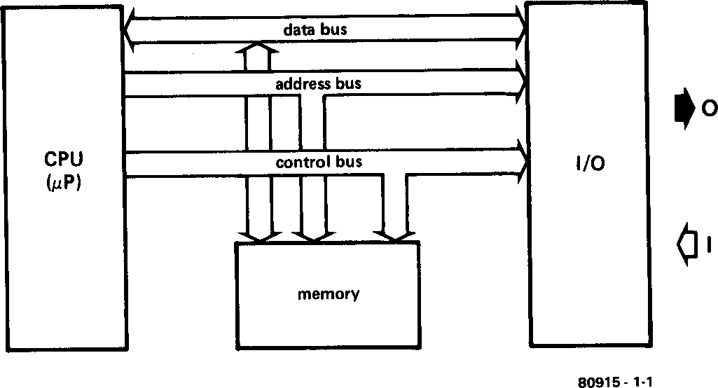
As can be seen from the block diagram in figure 1, a (micro) computer consists of three basic sections. These are the central processing unit (CPU), the input/output (I/O) section and the memory section. Information is transferred between the three ‘blocks’ by way of three groups of lines called buses, the address bus, data bus and control bus. A bus is quite simply a common line or collection of lines that are connected to more than one device.
Figure 1. The basic block diagram of a computer consists of three blocks and three buses. The latter provide the connections between the blocks.
A computer works with information, or data, which is in a form it can understand (specifically digital pulses). As its name suggests, the data bus carries this information to or from the various sections of the computer. The data bus consists of eight conductors and is therefore capable of transferring eight bits of data at a time. A bit is one piece of digital information or BInary digiT. A group of eight bits is commonly called a byte. The largest computer in the universe is totally useless unless it is able to communicate with the outside world. This is where the input/output (I/O) section comes into the picture. For humans to be able to understand what the computer has to say, and vice-versa, some form of translation medium has to be incorporated. This is usually carried out by means of a keyboard and video terminal, or some other form of display. However, this is not to say that communication is limited to these.
On to the memory. The memory is simply a store where the computer holds all the relevant information (instructions, data etc.) required for it to perform a particular task. There is no such thing as an ‘intelligent’ computer (not yet anyway — as far as we know!). A computer has to be told explicitly what to do and in what order. Date is stored in individual compartments in the memory. These compartments are usually referred to as locations and each has its own (unique) address. Via the address bus, the computer can pinpoint the exact memory location, and therefore the data, that is required. The address bus is also used to select the various input or output devices needed by a particular program.
Last, but by no means least, is the control bus. The control bus regulates various internal functions as well as telling the data bus which way to allow data to flow, whether to transfer data into or away from the CPU.
After looking at the block diagram of a ‘basic’ microcomputer, we move on to that of the Junior Computer (figure 2). First, the three buses. The address bus is formed by sixteen lines and is independent of the other two buses (the data bus and the control bus). With 16 lines, the CPU is capable of addressing up to 216 or 65,536 different memory locations. Thus, more than sixty-five thousand (or ‘65 k’) different pieces of data are at the computer’s ‘fingertips’ (provided, of course, this amount of memory is available).
The data bus consists of eight lines, but is bidirectional. This means that information can be moved in two directions, to or from the microprocessor. Of course, data can only be transferred in one direction at a time. The direction of data transfer is determined by the control bus. If the computer is told to read information then the control bus allows data to be transferred from the memory (or any other source) to the CPU. Conversely, if it is told to write information, the control bus allows data transfer from the CPU to the memory or any other device. The control bus does this via bidirectional data bus buffers which, according to control bus signals, allow data to pass in the proper direction only.
Memory comes in two main types, which is why there are two memory blocks in figure 2. One is RAM and the other is ROM. There are also two types of data: permanent (like a system monitor program) and temporary (most of the programs entered by the user). Permanent data therefore will only ever be ‘read", whereas temporary data has to be both ‘read’ and ‘written’. When talking about memory, the terms ‘reading’ and ‘writing’ refer to the act of seeing what is in memory and entering data into memory respectively. Memory that can only be read is called ROM or Read-Only Memory. Where a system monitor program is used it is invariably stored in ROM. Memory that can be written into as well as read from is called RAM, for Random Access Memory. RAM is used to store such things as intermediate results and programs which are under development. Random access memory is therefore often called work memory. The signal that controls the bidirectional data bus buffer mentioned earlier, also tells the memory whether it is going to be read from or written into, hence the term, READ/!WRITE.
It seems reasonable to point out at this time that when information is read from memory, that information is not lost. Similarly, the act of reading this page does not remove the text. The information is read and transferred to the brain (CPU) and further processed. RAMs do however forget when their power supply is cut off. When the information contained in RAM is to be saved for extended periods of time it is usually transferred to a more permanent form of data storage, cassette tape or floppy disc for example. This is more convenient and safer than leaving it in RAM. If the mains should drop out, all information in mains powered RAM would be lost.
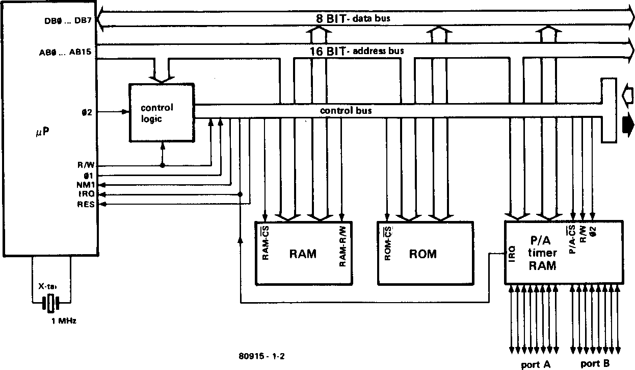
Figure 2. A detailed version of the block diagram in figure 1, this time with a specific computer in mind: the Junior Computer.
The block marked I/O maintains contact between the computer and the outside world. In figure 2 it is called PIA or Peripheral Interface Adapter. Just as with RAMs, bidirectional data transfer is necessary. The 8 bit data bus is passed out as two bundles of eight conductors each, through port A and port B. The active port is determined by the address bus. Each individual line can operate independently of the other 15 at any given moment, as an input or as an output.
Data can also be held at the PIA for short periods of time (notice that the RAM is in the same block as the PIA in figure 2). This facility can be used when the CPU has to do something else at the same time as data is being transferred through one of the ports. Information from either direction may be stored in this memory, but only from one direction at a time. The address bus informs the PIA which port, which direction, and whether or not to hold outgoing or incoming information.
There are also three buses that go to the outside (the three arrows pointing right in figure 2) but these are for future expansion of the system rather than communication with the outside world. As far as the JC is concerned, the outside world is everything beyond the keyboard and display.
The Central Processing Unit is the ‘heart’ of the microcomputer system. Briefly, the function of the CPU is to control the operation of all the other units and to process data. The CPU contains a number of registers which are used to temporarily store address, data and instruction information for decoding and manipulation purposes, etc.
The CPU also contains the program counter which simply counts the steps in the program. Its output can be fed onto the address bus in order to have access to the memory for the retrieval of program instructions. To determine the next successive address in a particular program, the program counter and the instructions already executed are analysed. Exactly how all this is carried out, however, is outside the scope of this chapter.
The microprocessor has a sort of built-in ‘pacemaker’ or clock, which is used to generate the timing pulses around which all operation is based. The two signals produced by this clock generator, Φ1 and Φ2, are 180° out of phase with each other. Without them the complete system would be useless, for they provide the ‘heart-beat’.
There are three other signals shown in figure 2, namely RES, IRO and NMI. RES is the reset signal and is virtually self-explanatory. This signal tells the Junior Computer to go to the ‘start’ condition. The other two, IRQ (Interrupt ReQuest) and NMI (Non-Maskable Interrupt), are used to modify or step through the program while it is being run. Information then comes from the outside to tell the computer what to do next. This feature can be useful when the computer is used with a relatively slow device (a human for instance). The computer can manage over half a million operations per second whereas the human may only be able to manage 3 or 4 during the same period. Once the interrupt is finished the computer will continue with the main program from where it left off. In the event that both of the interrupt functions are used at the same time, they are given a priority which is determined by the program. It should be noted that the interrupt request can be controlled by the program whereas, as its name implies, the non-maskable interrupt cannot.
A programmable timer can also be seen in the PIA block in figure 2. More attention will be given to this in chapter 5 (Book 2).
The keyboard and display complete the package. They are shown in figure 3. The keyboard consists of 23 key-switches and 2 toggle switches. Sixteen of these switches are used for entering information (in hexadecimal form) into the computer. The remaining keys are assigned various control functions. The display consists of six seven-segment LEDs and shows address and data information, again in hexadecimal form.
The keyboard and display are connected to the computer via ports A and B. Port A is designed for bi-directional data transfer whereas port B is unidirectional. There are two signals from the keyboard which are placed on the control bus, namely, RES and NMI. These belong to the keyswitches RST and ST respectively. More will be said about these when discussing operation. The sixteen lines from ports A and B are also connected to a 31 pin connector for future expansion.
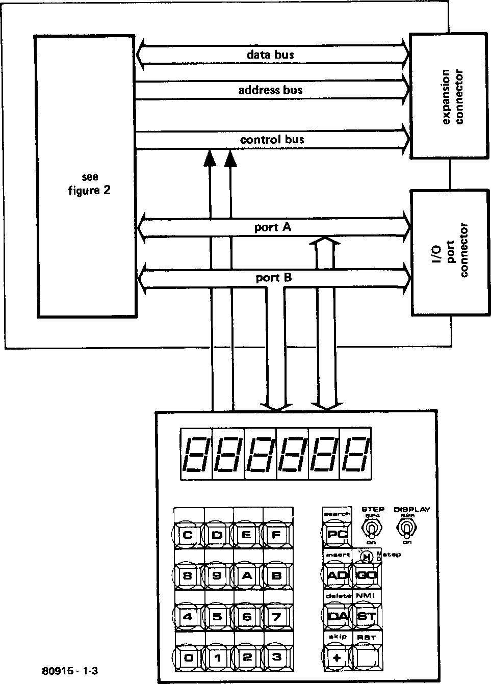
Figure 3. A further development of the diagram in figure 2:
communication with the outside world is now possible
with the aid of a keyboard to input (I = Input in I/O) data and
a display showing six hexadecimal figures to output (O = Output in I/O) data.
The address, data and control buses are accessible via a 64 pin expansion connector. The reason for these sockets is quite simple. Looking at it realistically, the hexadecimal keyboard as the standard input source, and the hexadecimal display as the output indication, are the simplest and least expensive methods of interacting with the computer.
There are also many other I/O possibilities, all fine and dandy, but they all require more money. Most beginners do not want to part with (or have) the kind of outlay required for more sophisticated input/output devices. Beginners, however, have a habit of becoming experts so the JC is designed to grow into an expert’s computer.
The 64 pin expansion connector may be used to expand the memory capacity of the system so that longer and more complex programs can be run. This is practically a necessity for more ‘grown-up’ computers (you never seem to have enough memory). Bearing this in mind, the expansion bus was designed to be compatible with the Elektor SC/MP system bus.
Now for a more detailed look at the Junior Computer’s electronics, the so-called hardware. It can be said that the hardware is the ‘flesh and blood’ of the computer and that the programs form its ‘personality’.
The circuit diagram of the Junior Computer is shown in figure 4. The CPU (IC1) is a 6502 microprocessor. Readers unfamiliar with the various types can be assured that the 6502 is a fast, high quality device. It has a ‘powerful’ instruction set with a great variety of (useful) programming possibilities.
The microprocessor needs something to ‘keep the blood flowing’: a clock generator. This is constructed using N1, R1, C1, D1 and a one megahertz (1 MHz) crystal. Two clock signals are generated, Φ1 and Φ2, for the address bus and data bus respectively. The address bus consists of lines A0 … A15 while the data bus consists of lines D0 … D7.
The electrical signals on the address and data buses are coded digital information. What is this code? Imagine a numbering system with only two numbers 0 and 1 as opposed to the normal ten: 0 . . . 9. The numbers nought and one are represented by ‘0’ and ‘1’ respectively (no change), but the number two is shown as ‘10’. Three is represented by ‘11’, four by ‘100’ etc. This is shown below for the numbers 0 . . . 15. Note: 0 is used for ‘zero’ to avoid confusion with the letter O.
decimal number		binary equivalent
	0		0000
	1		0001
	2		0010
	3		0011
	4		0100
	5		0101
	6		0110
	7		0111
	8		1000
	9		1001
	10		1010
	11		1011
	12		1100
	13		1101
	14		1110
	15		1111
As can be seen, the limit for 4 lines of binary data is reached with only sixteen combinations, whereas with a normal base ten count ten thousand combinations are possible (0. . . 9999). As was said earlier, the address bus has sixteen lines or 216 (65,536) different combinations. Therefore the limitation imposed by working with a number system with two as its base does not really pose a problem.
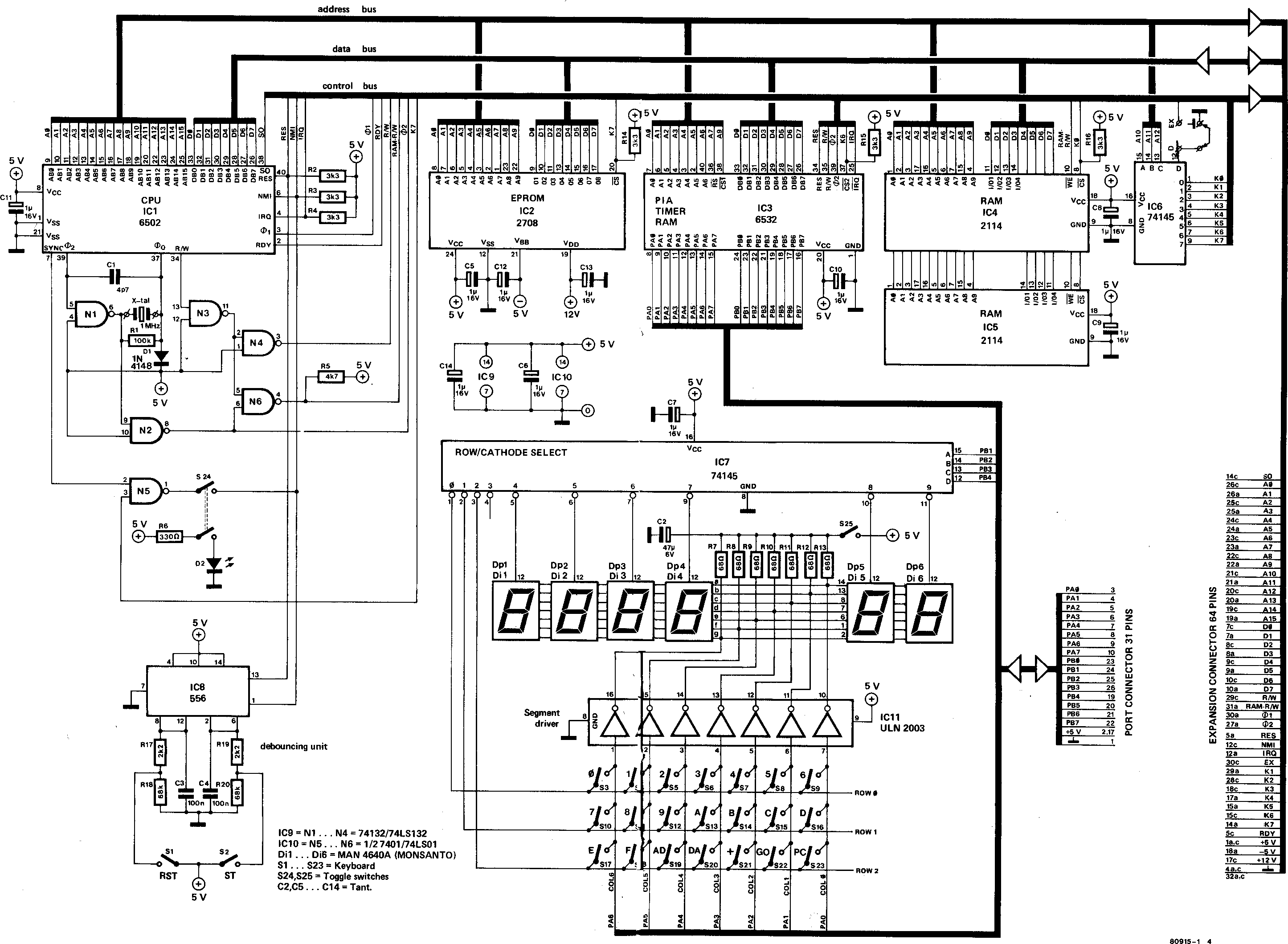
Figure 4. The complete circuit diagram of the Junior Computer.
To make things clearer, the buses have been drawn as a single line.
You will soon become familiar with the memory organisation of the Junior Computer once you gain further insight into the way in which memory operates in a computer system. In figure 4 the memory consists of two blocks of RAM and one block of EPROM (Erasable Programmable Read Only Memory). The EPROM (IC2) is for storage of permanent data (the system monitor program) and the RAMs (1C4 and IC5) are for operational use. Data transfer is accomplished in 8-bit blocks, or one full byte at a time. The EPROM has the capacity to store 1024 of these 8-bit groups. In computer terminology this is a 1 k byte EPROM (k meaning kilo or thousand). The various bytes have to be available on request, thus there are ten address lines connected to it giving 210 or 1024 different combinations. Strange coincidence that this should be the same number as the capacity of the memory!
The RAMs have a capacity of 1024 half-bytes, but, as there are two of these, their total capacity is 1024 full bytes (the same as the EPROM). The data bus lines are arranged so that the first half (four bits) of the data is in IC4 and the second half is in IC5.
The memory also receives directions from the control bus, selection signals for instance. The EPROM and the RAMs are connected to the same address lines, so how does the right one operate at the correct time? Both types of devices have a Chip Select (!CS) input. When this input is taken high (+5 volts or logic “1’) the memory is disabled. Conversely, if the input is taken low (zero volts, ground or logic ‘0’) the memory is able to operate. These !CS signals are derived from the address decoder, IC6, and passed to the EPROM as K7 and to the RAMs as K0.
Ten address lines are utilised by the memory, leaving six. As 26 = 64, this means that if these are used as chip select lines, up to 64 blocks of 1 k each are addressable. This amounts to 64 k – not the 65 k mentioned earlier, due to the fact that all the numbers have been rounded off. The total still comes to 216 = 65,536.
With 64 ‘block address lines’ available, all memory addressing is done with the first ten address lines. In the basic JC only the first eight memory blocks are decoded, namely K0 … K7 from the address decoder. Three address lines (A10 … A12) are fed to IC6 which promptly decodes them into the eight lines required. The table below shows this to advantage.
A15…A13	A12	A11	A10	A9…A0	active:	memory block:
X	0	0	0	X	Κ0	1 k RAM (IC4, IC5)
X	0	0	1	X	Κ1	1 k external RAM, ROM
X	0	1	1	X	K3	1 k external RAM, ROM
X	1	0	0	X	Κ4	1 k external RAM, ROM
X	1	0	1	X	K5	1 k external RAM, ROM
X	1	1	0	X	Κ6	RAM in PIA (IC3)
X	1	1	1	X	Κ7	1 k EPROM (IC2)
‘X’ means ‘don’t care’ . In other words, its state may be either a ‘1’ or a ‘0’ to get the listed result.
Of the 64 k then, 8 k are directly accessible. To address more memory, the address decoder must be expanded.
In addition to the chip select signal, the RAMs require another signal that tells the memory whether information is going to be read from or written into RAM. This is where the R/!W line comes into the picture. If this line is taken high the memory is going to be read from, and if it is taken low information can be written into it. This signal comes from the NAND gate N6 and is a mixture of the Φ2 clock pulse and the R/!W signal of the microprocessor. This guarantees that no data can be transferred while the data bus is not stabilised.
A number of control signals have already been covered, the rest now follow. For correct operation both the microprocessor (IC1) and the peripheral interface adapter (IC3) have to be initialised. This is achieved via the reset signal RES. The reset line is normally held high by a pull-up resistor, R2. A reset is generated when the keyboard switch RST is pressed. Operation of the RST key triggers the timer in one half of IC8 which is used to suppress any contact bounce this key might produce. The output of the timer is connected directly to the reset line.
There are two ways in which a program being run can be interrupted by means of the non-maskable interrupt (NMI). The first one is provided by the STOP key S2. You will notice that this key uses the other half of IC8 for contact bounce suppression. The second is provided by the STEP switch S24. When this is in the ‘on’ position and the output of N5 goes from high to low, the NMI line (normally held high via pull-up resistor R3) is also taken low. This feature is important when wanting to step through the program ‘byte by byte’. It should be noted that as K7 is connected to one of the inputs of N5, the output of N5 will always be high when the EPROM is selected. As N5 is a NAND gate, if one of its inputs is low the output will be high. All this means, effectively, that you cannot step through the monitor program held in IC2.
The program can also be interrupted if the IRQ (interrupt request) connection between IC1 and IC3 is taken low. This line is again held high normally, this time by pull-up resistor R4. Not only can the IRQ facility be used manually, but it can also be used via the timer in the PIA. When utilised by the program in this way it is called a ‘software interrupt’. The NMI and IRQ lines are also accessible on the 64 pin expansion connector.
Also present on the control bus are the two clock signals Φ1 and Φ2 which control the PIA and RAM R/!W signals. As mentioned previously, these determine the direction of data transfer. Finally, the signals RDY and SO, neither of which is used in the basic JC, are for future expansion with dynamic RAMs, and the line EX (see IC6) is important when expansion of the address decoding becomes necessary.
The PIA is capable of transferring data in two directions via ports A and B. Each port has its own 1/O register and eight-bit data direction register. The information contained in the data direction register determines which of the individual port lines are to be used as an input or output. If a particular bit in this register is a ‘1’ the PIA is instructed to activate the associated output, whereas if the bit is a ‘0’ an input is activated. The contents of the data direction registers is determined by the program or software. Actual data transfer is carried out via the R/!W signal. As with the RAMs, when this line is high a read operation is specified and data will be transferred from the PIA to the CPU. When the R/!W line is low, a write operation is specified and data will be transferred from the CPU to the PIA.
There is also a limited amount of RAM in the PIA, 128 bytes to be exact. Together with the 1024 bytes of IC4 and IC5 this gives a total of 1152 bytes (more than enough for the budding amateurs). Address lines A0 … A6 are used to gain access to the 128 bytes of RAM in the PIA. Address line A7 is connected to the RAM select input (!RS) of the PIA. In other words, when A7 is high the RAM is enabled and the CPU has direct access to it. When A7 is low the PIA RAM is disabled. Reading and writing to this RAM is, of course, controlled by the R/!W signal. The other address line (A9) connected to the PIA controls the selection of the I/O ports and the timer. When this line is high, address lines A0 … A6 determine which of the various functions of the PIA are to be used. For instance, port A or B enabled, direction of data transfer, access to the timer etc. Note that when A9 is high the PIA RAM cannot be accessed. The remaining signal connected to the PIA is K6 from the address decoder. The PIA is disabled (regardless of the condition of the other inputs) when K6 is high. The PIA is such a versatile and multi-functional device that we could quite easily write a whole book about it, but as far as this chapter is concerned, enough is enough.
The keyboard and display comprise the Junior Computer’s communication links (or peripherals) with the outside world. These are connected to port A by seven lines, to port B by four lines and to the control bus by two lines. The last two are the previously mentioned signals, reset and stop (RST and ST). Switch S24 has been mentioned before with relation to the NMH signal. It is also used to select either normal operation or step-by-step program development.
The other keys shown in figure 4 (S3 … S23) are arranged in a matrix of three rows and seven columns. Sixteen of these keys are used for entering data into the computer in hexadecimal code (to be dealt with in chapter 2). The word data has a broad meaning here as it also includes address information. The remaining five keys have been assigned various control functions. These will be discussed in depth in chapter 3.
Information going to the display, and data from the keyboard is transferred via seven lines of port A. In this instance it can be seen why bidirectional data transfer is very useful. The information on the displays is controlled by the software in the monitor program, which also ensures that key function signals are recognised. A BCD-to-decimal decoder, IC7, decodes the information presented on the four lines PB1 . . . PB4 from port B. This decoded information is used to multiplex the displays and check the state of the rows of keys to see which one, if any, is being depressed.
The first three outputs of IC7 are used to scan the keyboard. If a key is depressed while one of these outputs is high the code for that particular key is passed to the CPU via port A. The third output of IC7 is not used — it isn’t needed. When one of the remaining six outputs of IC7 is high, the appropriate display is turned on, and the coded segment information from the CPU is transferred via port A to the segment drivers contained in 1C11 and from there to the particular display concerned.
This process of successive selection of one device at a time is an elegant method of reducing the number of parts required for a particular application. Saving a few parts however costs a little software. The cost of the extra memory required, on the other hand, is far less than the cost of all the parts it would take to duplicate the functions it performs.
can be used in two different modes. Usually, the four left hand displays (Dp1 . . . Dp4) will indicate an address and the other two (Dp5 and Dp6) will show the data in the address location concerned. As a second possibility, Dp1 and Dp2 can show the hexadecimal code of an instruction (op-code) while the remainder show the address of the data corresponding to this instruction. The latter mode makes program entry much simpler.
The only other switch to be mentioned is the display turn-off switch S25. This comes in very handy for saving power if the JC is to be used with a terminal or other external device.
Even the most sophisticated of computers obviously needs a power supply. Three supply voltages are required by the Junior Computer and a suitable circuit is shown in figure 5. The three voltage levels are +5 volts (for all the ICs and displays), -5 volts and +12 volts (for the EPROM) and these are supplied by the voltage regulators IC1 … IC3. Each regulator IC has its own set of capacitors, C2 … C13, to ensure the necessary decoupling. Now that we have discussed the basic theory and operation of the Junior Computer we can start putting it all together.
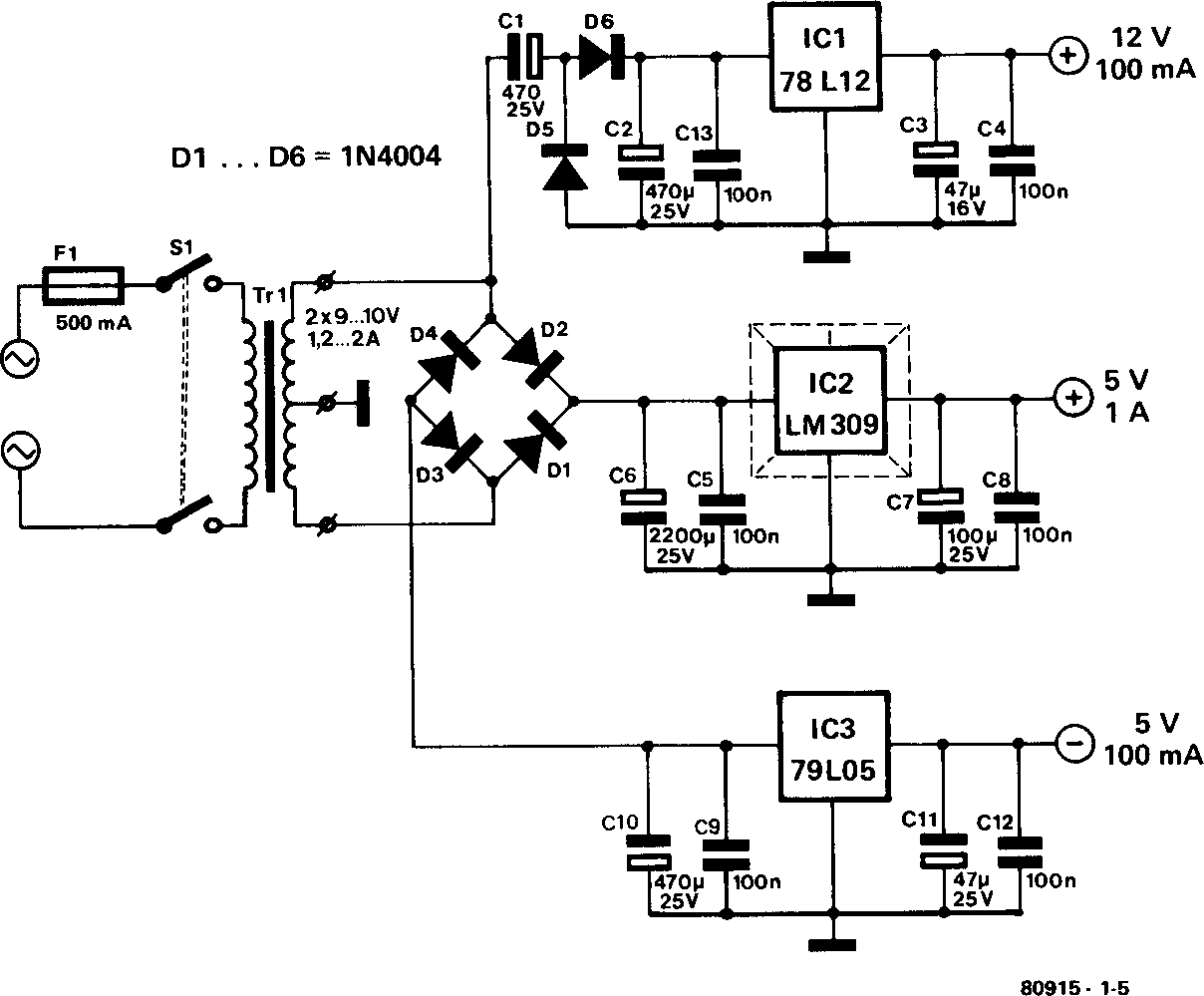
Figure 5. The power supply of the Junior Computer provides three stable voltages.
Where do we start? To make assembly as simple and as trouble-free as possible, this section should be read with extra care and attention.
Construction is accomplished in three basic steps. First, the components are mounted on the printed circuit boards. As the main printed circuit board is double sided, we do not advise readers to make it themselves. All boards are directly available from Elektor (EPS Nos. 80089-1,80089-2, 80089-3). Once the boards are complete and correctly interconnected, it is time to test them. This is the second and (hopefully, with good quality parts) fastest step. The third and final step is the mechanical assembly: putting the Junior Computer in its case.
The Junior Computer is very simple to construct as it is a single board computer. That is to say, all the electronic parts are mounted on the same board. Now sceptics may say: “there are three boards, how can you possibly call it a single board computer?”. The answer to that is quite simple. One of the boards is a power supply and so we don’t count it! Two remain, the main board and the display board. The latter is a small board carrying the displays and is attached to the main board. It could easily have been designed as part of the main board but that would have made it bigger and this way the displays can be tilted at an angle of 45°, making for better readability.
The main board is double sided, that is to say, there are copper tracks on both sides of the board and, in this case anyway, components on both sides too. Certain copper tracks on one side of the board are connected to copper tracks on the other side. This is possible because the board has ‘plated through’ holes. Before any assembly is started it is a good idea to check all the plated through holes (there are over six hundred of them!). This can be done with the aid of an ohmmeter, or (if you don’t posses an ohmmeter) by means of the inexpensive method shown in figure 14a. The low voltage secondary of a bell transformer is used in series with a doorbell to indicate continuity. Using two pieces of wire, one on the top side of the hole and the other on the opposite side, if the bell sounds the plating is good. This method has one advantage over the ohmmeter — you don’t have to look at the scale every time to confirm a good connection. If a hole should happen to be found to have defective plating, it can be remedied by soldering a wire link in its place or by simply using the lead of the component to be soldered in that hole. All this may take a little time but it could save a lot of frustration later.
The two sides of the main board are, of course, very different. The component overlay for the top side is shown in figure 6 and that for the bottom side in figure 7. Figures 8 and 9 show the track layout for the top and bottom sides respectively. The keyboard and display board are mounted on the top side of the board and all the rest of the components, excluding the power supply, are mounted on the bottom side.
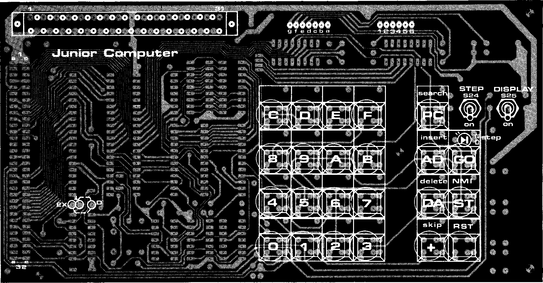
Figure 6. The component overlay of the keyboard section of the Junior Computer (EPS 80089-1)
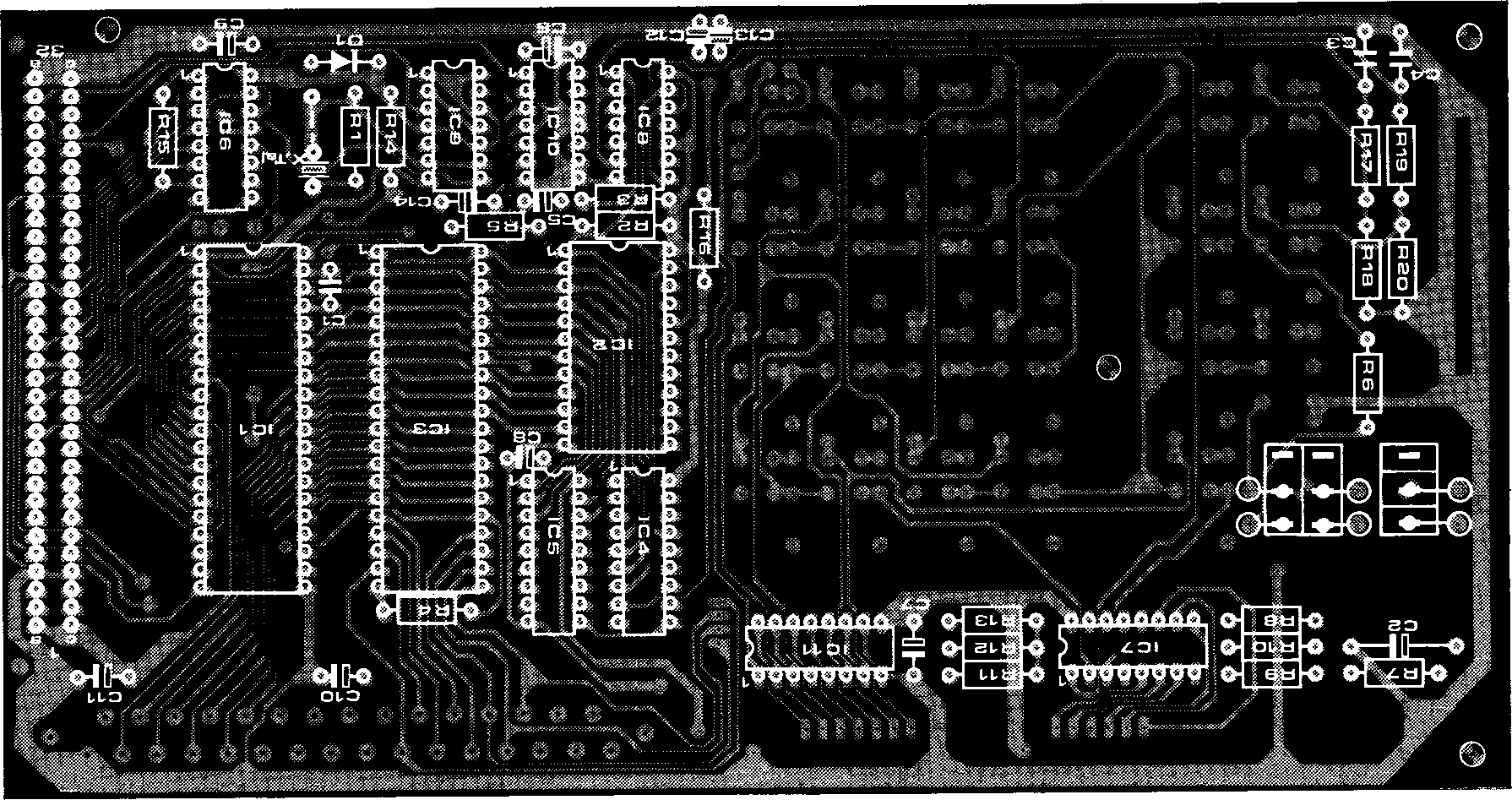
Figure 7. The overlay of the component side of the main printed circuit board.
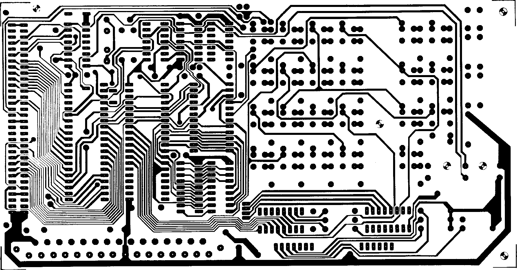
Figure 8. The track pattern of the upper side of the main board.
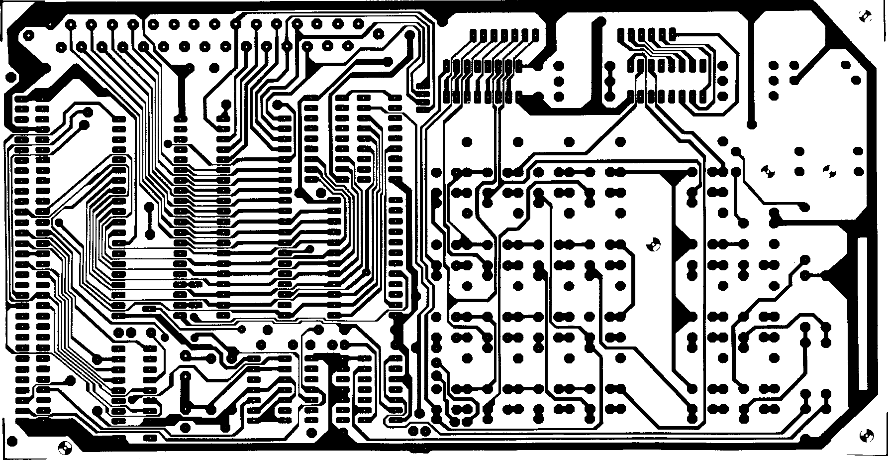
Figure 9. The track pattern of the lower side of the main board.
The complete circuit diagram is shown in figure 4, the two component overlays are given in figures 6 and 7 and the two track patterns in figures 8 and 9.
R1 = 100k
R2,R3,R4,R14,R15,R16 = 3k3
R5 = 4k7
R6 = 33ΟR
R7 … R13 = 68R
R17, R19 = 2k2
R18,R2O = 68k
C1 = 10p ceramic
C2 = 47µ 6V tantalum
C3,C4 = 100n MKH
C5 … C14 = 1 µ/35 V tantalum
IC1 = 6502 (Rockwell)
IC2 = 2708
IC3 = 6532 (Rockwell)
IC4,IC5 = 2114
IC6, IC7 = 74145
IC8 = 556
IC9 = 74LS00, 7400, 74LS132
IC10 = 74LS01, 7401
IC11 = ULN2003 (Sprague)
D1 = 1N4148
D2 = LED (red)
S1 . . . S21 S23 = digitast (Shadow)
S22 = digitast + LED
S24 = double pole switch
S25 = single pole switch
connector 64-pole   male perpendicular solder to DIN41612
connector 31-pole female perpendicular solder to DIN41617
1 MHz-crystal
1 × 24-pin IC sockets
2 × 40-pin IC sockets
1 printed circuit board EPS 80089-1
Now assembly can begin in earnest. The soldering iron used should have a ‘pencil’ tip and be in the 20-30 Watt range. The components should be mounted in the following order (see figure 7 and the full parts list for the main board):
The resistors R1 … R20 are the first components to be installed. After soldering, the excess lead length should be cut off as close to the surface of the printed circuit board as possible. This is a logical safety measure, to prevent shorts between adjacent connections. For those readers who are unfamiliar with the resistor colour code the corresponding colours for the values used are listed below.
100k:	brown-black-yellow (gold)
3k3:	orange-orange-red (gold)
4k7:	yellow-violet-red (gold)
330R:	orange-orange-brown (gold)
68R:	blue-grey-black (gold)
2k2:	red-red-red (gold)
68k:	blue-grey-orange (gold)
The first ring is the ring closest to one of the ends. The fourth ring indicates the tolerance (how much above or below the actual value it may be) of the resistor. Most resistors will have a gold ring which indicates a tolerance of ±5%. It is possible (though unlikely) to get a 1% (brown) or a 2% (red) resistor. If one of your resistors has a fourth ring of silver (10%) it should not be used. Another resistor will have to be found with a tolerance of ±5% or less to take its place.
The next component to be installed is the diode D1. Care must be taken to connect the diode the right way round. Its polarity is usually given by a ring around one end of the diode case. This ring denotes the cathode (the cathode is the thick line at one end of the triangle in the circuit diagram). In the unlikely event that the diode does not have a ring at all, or it has a ring exactly in the centre, the only positive way to determine its polarity is with an ohmmeter. When testing with an ohmmeter, it will be found that the diode exhibits a rather high resistance in one direction and a much lower resistance in the other. This only tells you that the diode is a good one, it does not tell you its polarity. The next step is to measure a diode with a known polarity and note which probe is connected to the cathode when the diode conducts. If no known diode is available then usually the red probe of the ohmmeter is the cathode when the diode conducts.
The capacitors C1, C3 and C4 are now installed and their excess leads cut off.
The electrolytic capacitors C2 and C5 . . . C14 are then mounted. Normally with capacitors and resistors you can install them regardless of their polarity. This is not the case with electrolytics. These have a positive and a negative side. In the circuit diagram the negative side is shown as a shaded (▮) rectangle and the positive side as an empty (▯) rectangle. On electrolytics that do not have a plus sign, the positive end is identified in one of two fashions. Either one end has an indented ring or the positive lead has a red mark.
The next items to be soldered in are the sockets for the ICs. We recommend that sockets be used for all the ICs but, as these are an added expense, it is possible to mount the smaller ones directly onto the board. Sockets are essential for IC1 … C3. There are of course two ways to mount an IC (if you guessed a right way and a wrong way you are not far out!). On the parts layout (figure 7) there is a ‘notch’ at one end of every IC. if you look at the drawing of an IC with the notch at the top, then pin one is at the top left hand side. This is also indicated on the layout. The numbering of the pins goes down the left hand side and continues up the right hand side. So for a 14 pin IC the lower left is pin 7, the lower right is pin 8, and the top right is pin 14. As far as the IC itself is concerned, the ‘notch’ can take various forms. It could be (and usually is) a notch just like that in the parts overlay, but it could also be a ‘dot’ impressed in the body of the IC. This ‘dot’ denotes pin 1, and the IC should be installed with the dot on the same side as in the parts overlay. Not quite so important but very very useful is the fact that IC sockets also have pin 1 marked in some way or other — the socket can be the wrong way round as long as the IC inserted into it is the correct way round.
The 1 MHz crystal can be mounted directly onto the board, or a crystal holder can be used.
This step is optional. As it is not likely to be needed just yet, the 64 pin expansion connector can be installed at a later date. When mounting the connector be sure to ‘screw it down tight’ before soldering any of the pins. If, however, you delay installation of the connector, provision must be made for the supply lines. These would otherwise use the expansion connector to come onto the main board. The power supply connections are:
+5 volts: pins 1a or 1 c
ground (0 volts): pins 4a, 4c, 32a or 32c
-5 volts: pin 18a
+12 volts: pin 17c
The obvious solution is to use terminal pins as a temporary connection medium but care must be taken when de-soldering the pins, as the copper track is very thin in places and may lift off if excessive heat is applied. That completes the mounting of components on the bottom side of the board, and now it is the turn of the keyboard side.
The only wire link on the board should be mounted next. It should be soldered between the points marked (⊥) and (D).
The two toggle switches (S24 and S25) can be installed next. These should be mounted so that the switch housings are on the underside of the board. The switches are connected to the main board by six short flexible insulated wire links. The positions for these are clearly marked on the underside of the board.
If required, the 31 pin connector can now be soldered into place.
The keyboard is next, along with D2, Care should be taken when installing the key switches, they should lie flush with the printed circuit board. D2 is mounted inside the ‘GO’ key. Remember, even though it is an LED, it is still a diode, and its polarity will have to be determined. The method described in part 2 can also be employed here.
That completes construction of the main board, or does it? It certainly won’t hurt to check all the ICs, diodes, and electrolytic capacitors for correct polarity, and every component for proper placement. Above all check your soldering for bridges between tracks, dry joints, etc. Soldering mistakes are still the biggest headaches on home-built electronic equipment.
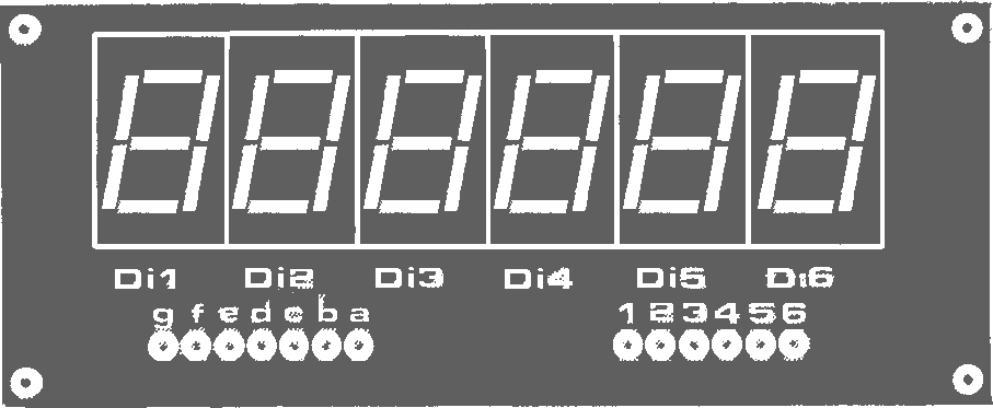
The component overlay and the track layout for the display printed circuit board (EPS 80089 - 2) are shown in figures 10 and 11 respectively. There are really only two steps involved in the construction of this board: mounting the six seven-segment displays and connecting the display board to the main board. The displays should not present any problems as there is only one way to mount them — they have an asymmetrical pin-out. The connection to the main board consists of thirteen conductors: seven for the segment drives and six for the display drives.
These connections are labelled on the main board above the keyboard assembly. The distance between the two boards should be about 5 mm. The thirteen wires should be gauge and 1 to 2 cm long. They should be soldered onto the display board so that they protrude from the copper-clad side. It is advisable to check the component overlay as well as the printing on the main board when connecting the two boards to each other. Mount (but do not solder) the display board onto the main board. The display board should be tilted at an angle of approximately 45° relative to the main board. The wires can now be soldered and any excess lead length cut off.
Note: If it is more convenient, the display can be mounted at some remote location. So-called ‘ribbon cable’ is ideal for this. This is a flat set of conductors which are colour-coded for easy connection. It goes without saying that extreme care must be taken to ensure that the leads are not mixed up.
|
Figure 10. The component overlay of the display board (ΕΡS 80089-2).
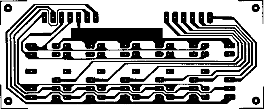
Figure 11. The track pattern of the display board.
The component overlay is shown in figure 10 and the track pattern in figure 11.
Di1 … Di6 = ΜΑΝ 4640Α common cathode (Monsanto)
1 printed circuit board ΕΡS 80089-2
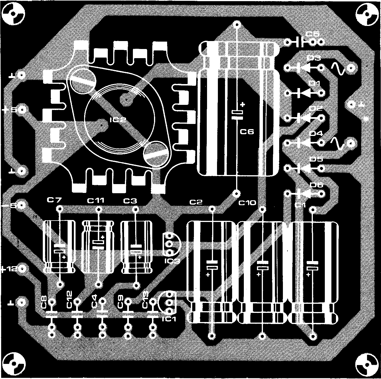
Figure 12. The component overlay of the power supply board (EPS 800-89-3).
The circuit diagram is shown in figure 5 and the board is given in figures 12 and 13.
C1,C2,C10 = 470µ/25V
C3,C11 = 47µ/25V
C4,C5,C8,C9,C12, C13 = 100n MKH
C6 = 2200µ/25V
С7 = 100µ/25V
IC1 = 78L12ACP (5%)
IC2 = LM 309K
IC3 = 79L05ACP (5%)
D1 … D6 = 1N4004
Tr1 = transformer prim. 220 V sec. 2 x 9 … 10 V/1.2 … 2 A
S1 = double pole switch
F1 = fuse 500 mA, with fuse holder
1 printed circuit board EPS 80089-3
1 finned heat-sink for IC2
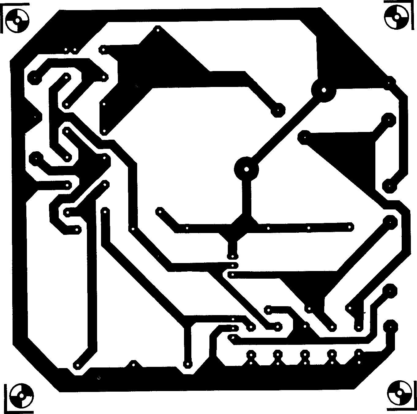
Figure 13. The track pattern of the power supply board.
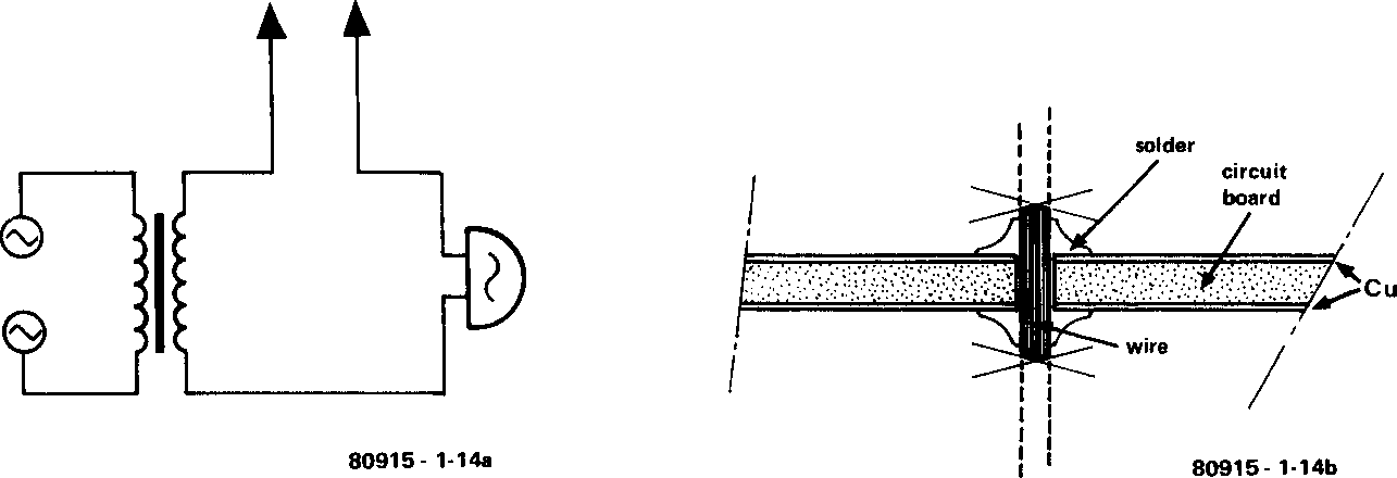
Figure 14. The electrical connections need not necessarily be tested with a multimeter (ohmmeter); it can also be done acoustically with the aid of an inexpensive bell and bell transformer. Note: this method may only be used if the components have not yet been mounted on the board. Figure b shows how to connect the two sides of a home-made board (which has not got plated through holes) with a vertical wire link.
The component overlay and track pattern for the power supply board are shown in figures 12 and 13 respectively. Like the display board, the construction of this board should not present any problems. Care should, of course, be taken to ensure that the diodes and electrolytic capacitors are mounted with the correct polarity. A heat sink is required for IC2 (the LM 309K).
The three boards are now complete. The next stage is to connect the transformer Tr1 to the supply board, and via switch S1 and fuse F1 to the mains. Since in the up-coming test phase operation is going to be temporary, it can be jury-rigged at this stage. This does not mean that it should stay that way. Before starting the test procedure it is advisable to check all the components once again. It is better to be safe than sorry. Perhaps you are able to find someone else who is able to give the circuit a look-over (another set of eyes often finds things previously overlooked).
The first thing to check is, of course, the power supply board (do not connect it up to the main computer board yet). Plug it in. No puff of smoke? A good sign! Oh, you forgot to switch S1 on. Stili no smoke? If the answer to this question is no, the power supply has just passed its first test. Measure (with a multimeter set for DC volts) the supply output voltages. The readings should be within 5% of the rated output. If the supply voltages are outside their allowable limits something is obviously amiss. This is very unlikely, however, owing to the quality of components and simple design of the circuit.
If the power supply checks out all right, the wires between it and the main board can be soldered into place. Make absolutely sure that the wires are connected correctly. Double check, triple check, you’ll only have yourself to blame if it is wrong. Once you are sure everything is connected correctly set switches S24 (STEP) ‘off’ and S25 (DISPLAY) ‘on’. You now apply power once again and . . . nothing happens. Don’t panic — this is what is supposed to happen. Now press the reset switch (RST). If all is in order the displays should give a clear hexadecimal number. To understand what is going on you will, of course, have to learn about the hexadecimal code given in chapter 2. For the time being you only have to compare the readouts with figure 15. The displays should show a random combination of these expressions. Readers who have already digested chapters 2 and 3 will recognise this as a sort of conditional jump instruction. If the display has the above, the next section can be skipped and you can move on to the mechanical assembly.
 |
 |
 |
 |
 |
 |
 |
 |
| 0 | 1 | 2 | 3 | 4 | 5 | 6 | 7 |
 |
 |
 |
 |
 |
 |
 |
 |
| 8 | 9 | A | b (=B) | C | d (=D) | E | F |
Figure 15. When the RST key is depressed the display should show a (apparently) random combination of the above hexadecimal figures.
This shows the Junior Computer is working properly.
We sincerely hope this section will not have to be read, but just in case something is wrong the most common faults and how to deal with them are listed below. The first thing to check is the power supply voltages. Although these have already been checked, there may be something on the main board which is causing problems.
Solder shorts. Solder forming a bridge between adjacent tracks. They don’t always have to be obvious either. Hair-line solder bridges can be very troublesome.
Bad solder joints. ‘Dry joints’. They can happen to anyone and are typified by a ‘shattered’ surface and poor contact with the copper track. If one is found, touch the joint with the soldering iron and apply a little additional solder.
Bad IC socket connection. It can happen. Poor contact between the IC and the socket. A careful inspection may even reveal a pin bent underneath the IC, not going into the socket! It is rare, but possible to have dirty contacts in the socket itself. If pushing down on the IC causes correct operation, then this is almost certainly the case. A little alcohol, on a cotton-bud, brushed over the top of the socket (allowing some to run into the socket) will usually remedy this.
Bad tracks on home-made printed circuit boards. This could be caused by insufficient or too much time in the etchant or by hairs on the artwork. Problems with the through-board connections should have been eliminated if the board was tested as outlined earlier.
Incorrectly installed diodes, electrolytic capacitors or ICs. If ICs are in the wrong position or mounted the wrong way round this will, obviously, cause the JC to malfunction. Are the connections between the main board and the power supply board correct and good? Between the main board and the display board? Up to now nothing but ‘normal’ items have been discussed. Here are a few special hints:
Measure the voltage between pins 13 and 7 of IC8 (pin 7 is negative and pin 13 is positive). It should be +5 volts. Press the reset button (RST) on the keyboard, the voltage between those two pins should now be approximately 0.5 volts. If this is not the case the problem could involve one of the following parts: IC8 (the double timer), the pull-up resistor R2 or the reset switch itself.
If all checks out okay so far then measure the resistance between pin 12 of IC6 and ground (of course, whenever checking resistance the power should be turned off). It should be zero ohms. If not, then the wire link is in the wrong place.
The clock generator constitutes the heartbeat of the computer. With a dual-trace oscilloscope the signals (Φ1 and Φ2) on pins 30a and 27a of the expansion connector can be monitored. The earth of the scope should be connected to computer ground (pins 4a or 4c) and the A (or Y1) input to pin 30a and the B (or Y2) input to pin 27a. There should be two ‘out of phase’ signals on the screen. When one goes high, the other should go low and vice-versa. The peak-to-peak voltage should be somewhere between three to five volts. The scope should have no trouble keeping the signals steady. They should be stable. If any of the above is not true the culprits could be C1, C9 or D1.
Chances are that one of the above ‘trouble-shooting’ techniques will solve your problems; however, if you are still unable to get the Junior Computer up and running, you can call the Elektor technical staff on Monday afternoons for additional help (see latest magazine for details).
The case has three basic purposes: to protect the circuitry from the elements, to allow for convenient operation, and to make the computer look really smart.
There are two popular methods of building cases for projects: the ‘cigar box’ method and the buy-ready-made method. Ready-made small computer cases usually have a display panel. The display board of the Junior Computer can be mounted behind this once all the necessary holes have been made. A clearance hole for the keyboard and toggle switches will also have to be made in the upper surface of the case. The fuse holder and mains socket can be mounted at the rear.
The ‘cigar box’ builder will have to design the case to meet the above criteria. Keep in mind that in the future, various expansion boards will come along and the case will also have to accommodate these. The boards are mounted in the case using ‘stand-offs’. Be careful when installing the main board that the keyboard switches operate freely to avoid mis-entered information.
Now the fun can begin.