COMPUTE II ISSUE 3 / AUGUST/SEPTEMBER 1980 / PAGE 15
Nuts And Volts No. 3 Address Decoding
Gene Zumchak
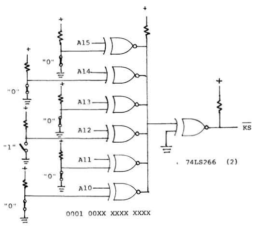
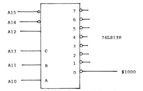
An important consideration in microprocessor system design is address decoding. Address lines are decoded from the highest order lines to subdivide memory space into smaller blocks. For example, the top three lines, can be used to divide memory into eight 8K blocks; the top four lines, into sixteen 4K blocks; the high six lines, into sixty-four 1K blocks; etc. There are numerous ways to do the decoding in hardware. If addresses need to be changed often, then dip switches and open collector Exclusive NOR (compare) gates can be used to compare any number of address lines with the selected polarity of that address line. The open collector outputs are wire-ORed together. If any gate is false the output will go low. An additional EX-NOR gate can be wired as an inverted to give a low true output. Figure 1. shows this method used to generate the 1K select for $1000 (000100). If the address decoding is to be permanent, a single 3 to 8 decoder like a 74LS138 can be used to give one, or several 1K, 2K, 4K, or 8K selects. Figure 2, shows a 74LS138 wired to give a select for $1000. Still another method is to use a 4-hit magnitude comparator chip, like the 74LS85. These can be used with switches on one of the word inputs, and also can be cascaded to compare longer words.
For 6502 systems, some users use Ø2 as an input to address decoders. This transfers the strobe action required for writing from the write input to the chip select. It also means that “reads” will be gated with Ø2. The user can get away with this only because the hold time requirement for the 6502 on a read operation is so short. As mentioned in the first column, if Ø2 is seriously delayed via the address decode paths, the strobing action could occur after the write data has already gone away. In general, it is not the best practice to “gate” write data with the strobing signal.
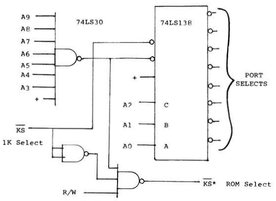
For ROM selects, it is desirable to gate in the R/W signal, so that the ROM select can never go true for a write operation. In the AIM, for example, ROM selects are generated from a 2 to 4 decoder. Ironically, this decoder has a gate input that was grounded instead of using the inverted R/W signal. If a write operation is attempted to ROM area, both the ROM and 6502 will attempt to drive the bus. Fortunately, most chips are designed to take momentary shorting and it is most unlikely that any harm will come to the 6502 or ROM. Still, it is careless design not to consider that writes may be attempted to read-only space.


Stealing Addresses
What does one do when a few addresses are needed for I/O ports? Is it necessary to waste a large chunk of space for a few addresses? Clearly, more address lines can be decoded so that decoding is complete.
Still, it is questionable whether that helps much, since if the remaining space is to be used, it will have to be decoded to exclude those addresses. If you have space set aside for ROM, however, and if you won't need every last word, then it is possible to steal a few addresses for I/O without having to waste any other space. Suppose we have a 1K select at $1000 which we will use for ROM. The circuit of figure 3 steals the top eight addresses of a 1K select. The ROM will respond only to 1016 addresses. The top eight addresses generate eight I/O selects with a 74LS138.
When designing 6502 controllers from scratch, the address stealing method illustrated can be used to extract I/O addresses from zero page. Rarely is all, or even half, of zero page needed for scratch pad. Putting I/O in zero page not only can considerably cut program length, but also speed up execution time. In some of my early controller designs, I used a pair of 256 × 4 RAM chips, and decoded addresses so that the RAM straddled pages zero and one. The low half of page zero was thus available for I/O.
Special 6502 Address Considerations
All 6502 systems have two address decoding needs in common. First of all, a select must respond to the very highest addresses where the reset and interrupt vectors are located. (It is too bad that one of the unused pins on the 6502 could not have been used for an open drain vector select. This would have allowed the user to wire-OR this select with his own ROM area for response to the reset and interrupts.) The other consideration, of course, is that all 6502 systems need RAM in zero page and page one (for stack).
Interestingly, the KIM, SYM, and AIM use three different methods for interrupt response. The unexpanded KIM avoids the interrupt vector problem by not decoding the top three address lines so that every 8K block is the same. Thus the unexpanded KIM responds to $FFFC at $1FFC. If a KIM is expanded, its address decoder must be enabled only in the lowest 8K block. The interrupt vector area must be decoded with an open collector decoder and wire-ORed to KIM's K7 select ($1C00-$1FFF). The SYM causes the response to the reset vector to be ROM at $8FFC, but the response to the interrupt vectors to be the system RAM at $A600. How does it perform this magic?
The SYM's reset lines go as usual, to the VIA port chips. All I/O lines on the VIA port chips come up in a high state at rest. The CA2 line of one of the VIAs is inverted to give a low-true Power On Reset signal which is effectively wire-ORed to the monitor ROM. Thus upon power up, the SYM finds the reset addresses at $8FFC and $8FFD, not because of decoding, but because the monitor ROM is held fast enabled by the POR line. One of the first things the reset program does is to reset the POR line. This line also inhibits normal address decoding. After POR is reset, normal address decoding takes place, and response to the interrupt vectors will be to the system RAM area (which is preloaded with default interrupt vectors at reset time).
The AIM'S solution is the simplest. It merely puts its 8K monitor in the highest 8K block of memory. Thus the reset and vector select is the normal ROM select.
The KIM, SYM, and AIM can all be used as the basis for dedicated controllers. In such an application, it is usually desireable for Reset to cause the user's controller program to begin. For either the KIM or SYM this is no problem. The KIM will require external decoding of the reset vector space. The decode can be wire-ORed to the controller's ROM. The SYM allows the POR signal to be alternatively jumpered to any of the on board ROM sockets. The AIM, unfortunately, will require that some cutting be done to the board, and further decoding tacked on, so that monitor programs can still be used, without the monitor responding to the topmost vector addresses. For any of the three systems mentioned, when using them in a controller application, some input condition should be defined which will cause the program to enter the board's normal monitor programs.
SummaryAddress decoding uses the highest address lines to subdivide memory space into smaller chunks. Selects are used to enable RAM, ROM and I/O. Address selects can use Ø2 as an input, thus including the strobing action required for writing in the select. ROM selects should include the R/W signal so that they will not respond to write operations. Address stealing can be used to obtain port selects from ROM area without wasting a large chunk of memory space. Similarly, I/O addresses may be stolen from zero page RAM area. Various methods can be used to respond to the Reset and interrupt vectors at the top of memory space. A particularly versatile method is the Power On Reset used on the SYM.
I welcome any comments or criticisms you may have of the material in this column. I invite your suggestions for topics for future columns. However, time and space do not allow major design projects for the column.